A PCB layout engineer knows that a well-crafted PCB layout is the cornerstone of producing a reliable and cost-effective end product. Although circuit design and component selection are important factors, dedicating sufficient time and expertise to the PCB layout process is crucial to achieve a successful outcome. This is especially true as boards become more complex, smaller and lightweight, with the increasing use of flexible PCBs only adding to the design challenges.
Creating a PCB layout is akin to an artistic process where engineers can spend significant amounts of time, sometimes ranging from days to months, intricately designing patterns that are both unique and optimized for functionality. However, a proper PCB layout is not solely the domain of trained engineers; with appropriate guidance and practice, anyone can create effective layouts.
This article aims to provide an overview of essential aspects of the PCB layout process. Although initially daunting, starting with simple designs and dedicating adequate time to learning and practice is pivotal to mastering increasingly complex designs.
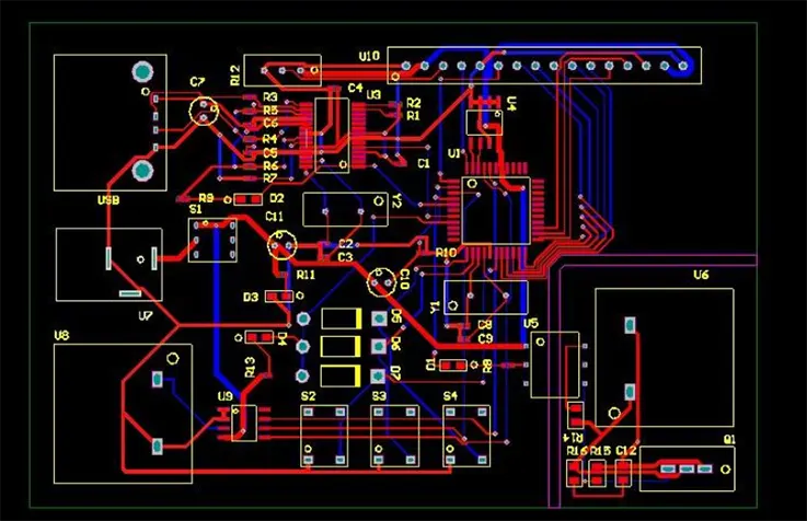
What Is the PCB Layout?
The PCB layout is a fundamental aspect of printed circuit board design, encompassing component placement, routing, trace width, and spacing, among other crucial considerations. As PCBs are ubiquitous in a wide range of industries, including consumer electronics, information technology, telecommunications, healthcare, and aerospace, the quality of the PCB layout is critical for achieving the desired functionalities and performance metrics of electronic products. Overall, designing an effective PCB layout requires a deep understanding of electronics, manufacturing processes, and best practices in PCB design.
The Basics of PCB Layout
When using PCB design software to create schematic diagrams, it is crucial for an electronic design engineer to possess a thorough understanding of electronic device abbreviations. This is because the first three letters of various electronic terms are commonly used to indicate a particular device or component, such as RES for resistor, CAP for capacitor, and IND for inductor.
Furthermore, it is important for electronic design engineers to grasp the essential terminologies related to voltage, current, ohm, volt, ampere, watt, circuit, circuit element, resistance, resistor, inductance, inductor, capacitor, Ohm’s law, Kirchhoff’s law, Kiel Hough voltage law (KVL), Kirchhoff’s current law (KCL), loop, network, passive two-terminal network, and active two-terminal network. Such knowledge is a basic requirement for creating accurate schematics that facilitate efficient manufacturing and assembly processes and ensure the reliable performance of electronic products.
How to Design a PCB Layout ?
A drawing frame is an essential schematic template utilized in generating schematics for PCB design. Various sizes of schematic templates are included in numerous PCB design software packages, alleviating the need to begin a design starting from scratch. In the event that electronic design engineers need to standardize the format within their team or modify the attributes, the drawing frame wizard within the software can be utilized to create a new template. This functionality allows for improved team collaboration while maintaining consistency in the design process.
Electronic design engineers must follow a specific process to create a schematic design:
● The first step is to construct a symbol on the schematic sheet that represents the component.
● Next, the components that will be used in the PCB layout must be designed. To achieve this, a “footprint” component concept is utilized, where a PCB footprint is constructed by placing connecting pads and silkscreen to define the component shape and position. The component parameters must be defined, including characteristics such as the manufacturer’s name, part number, and operating temperature.
● Once the schematic template and components are created, the schematic components must be placed on a schematic sheet, followed by connecting them using wiring. An ERC/DRC verification should then be performed to ensure that there are no errors in the connections or layout.
● Finally, a BOM file must be generated for procurement.
After the schematic design is complete, engineers can begin designing the PCB. This involves defining the board size, placing mounting holes and dimensions, and positioning components.
● The next step is to route traces and create planes for power and ground nets. A DRC/MRC verification must then be performed to ensure that there are no breaches in design or manufacturing rules. Any errors discovered during the DRC/MRC process must be corrected to complete the design.
● Finally, Gerber and NC drill files must be generated to hold all of the information about the particular layers and designate where and how big each of the drill holes should be. By following this process, electronic design engineers can create high-quality PCB designs that meet the desired objectives and performance specifications.
In order to produce a PCB, certain files are required to be exported. It is crucial for electronic design engineers to pay close attention and ensure that the exported files are accurately prepared, as any faults in this phase may lead to costly repercussions during the manufacturing process. Accurate export files are essential to ensure that the PCB manufacturer can create a precise product that meets the required specifications. It is suggested that electronic design engineers review all exported files thoroughly to avoid any errors that may lead to additional time and expenses.
Importance of a Good PCB Layout
● Printed Circuit Boards (PCBs) are the backbone of electronic systems. A good PCB design is necessary for a product to function well, be reliable, and maintain its performance over time. The PCB layout has a direct impact on how signals are transmitted, how power is distributed, and how components are arranged on the board.
● A poorly designed PCB can result in common issues like failed solder joints, electromagnetic interference (EMI), crosstalk, or excessive heat generation. These problems can lead to significant product failures, increased manufacturing and troubleshooting costs, and even customer dissatisfaction.
● On the other hand, a well-designed PCB can enhance signal integrity, reduce noise, and provide an efficient and reliable power delivery system. This will ensure that the product performs as intended, meets industry standards, and can be easily assembled and maintained. Hence, a good PCB layout is essential for the success of any electronic product and should be given careful consideration throughout the design process.
Why Choose Us
JarnisTech: The Best One-Stop PCB Manufacturer in China.
With over 20 years of experience in PCB fabrication, we are well-equipped to rapidly provide our customers with complete Gerber and drawing packages. Our services are available to customers who require a PCB layout based on their design schematics. Furthermore, we are capable of updating, altering, or optimizing existing designs for cost-effective assembly. For customers who need a new PCB design created from concept to creation, our team is proficient in developing full PCB documentation, including schematics and BOM.
As a fully licensed PCB manufacturer, we utilize industry-leading software tools such as Cadence Allegro, Mentor Expedition, Mentor’s PADS, Altium, and Valor for DFM Analysis. Our highly skilled and experienced team of engineers and CAD/CAM operators are readily available to address any project requirements our customers may have. We take pride in delivering high-quality PCBs that meet our customer’s unique specifications and are committed to exceeding their expectations.
Our Capabilities include the entire design process, from conception to final product, including:
● EMI Checking.
● Schematic Capture.
● Rules Driven Designs.
● Library Development.
● Full Document Package Creation.
● Signal Integrity/Design Verification.
● Database Construction and Verification.
● Micro BGA / Micro Via / Blind and Buried Vias.
● Electrical Engineering: As a leading PCB manufacturer, we have extensive experience and a proven track record of consistently achieving the industry’s highest standards. Our expertise spans across various industries, including medical, datacom, telecom, computer and storage, military/aerospace, industrial, and consumer products.
We are dedicated to delivering exceptional products and services that meet or exceed our customers’ expectations. Through our expertise and commitment, we are confident in our ability to provide customized solutions that fulfill the most rigorous industry requirements. Regardless of the industry, our commitment to quality, reliability, and precision remains constant, allowing us to consistently deliver exceptional results.
● PCB Fabrication: JarnisTech, an established PCB manufacturer with over two decades of experience, takes pride in providing superior PCB solutions to our valued clients. No matter the complexity, our team of skilled engineers is available around the clock to deliver bespoke PCB services, from prototypes to production runs, to meet our clients’ specific requirements.
We offer a wide range of PCB solutions, including simple single-sided PCBs, HDI, sequentially laminated multi-layers, and multiple blind and buried vias. With a focus on client service, we specialize in manufacturing PCBs with various capabilities, such as via in pad, silver filled, copper filled, epoxy, conductive and non-conductive via fill, ENEPIG, aluminum, and RF.
At JarnisTech, our primary objective is to continue providing exceptional client support, which is why we continuously invest in advanced PCB production equipment. We take pride in fulfilling our clients’ needs with the utmost efficiency, quality, and speed.
PCB Layout Design Considerations
As a PCB layout designer, there are various crucial factors to keep in mind during the design process. While some factors apply to the entire layout and design process, others are specific to certain sections. Here are Four essential considerations to take into account:
1. PCB Board Constraints
● As a PCB designer, it is crucial to consider various constraints related to the bare board during the design process. These restrictions include the size and shape of the board, which are fundamental to achieving optimal performance, functionality, and reliability.
● The size of the board must provide sufficient space to accommodate the circuitry required for the end product. While electronic products and their corresponding circuit boards have become increasingly smaller in recent years, estimating the required board size before beginning the design process is essential. If the functionality required cannot be achieved with a simpler design, a multilayer or high-density interconnect (HDI) architecture may be utilized.
● While the rectangular shape remains the most common for PCBs, other form factors can be employed to suit specific size and shape constraints.
● The number of layers required is another critical factor to consider, determined by power levels and design complexity. Determining the required number of layers early in the layout planning process is recommended, as adding additional layers can increase production costs but allow for more integrated tracks, which may be necessary for more complicated boards with additional functionality.
● To ensure reliability, thermal conductivity, and lower inductive and resistive losses, using at least two vias for layer transitions for all high-current routes is recommended. The use of multiple vias at layer transitions is a practical technique for enhancing the overall performance of the board.
2. PCB Manufacturing Processes
● PCB design engineers must consider the manufacturing processes they intend to utilize during board creation, as different methods have varying constraints and limitations. Reference holes or points that are compatible with the manufacturing process must be incorporated into the design to achieve optimal results.
● Also, the board’s mounting method must be considered, and different portions of the board may need to be left open, depending on the approach used. Implementing various technology types, such as through-hole and surface mount components, can increase the cost of boards, but they are often necessary to achieve the desired functionality.
● It is crucial to verify with the fabricator to ensure that they can build the type of board required. It is possible that not all PCB manufacturers have the capability to create boards with multiple layers or flexibility in design. Hence, having a clear understanding of the manufacturer’s capabilities before the design process begins is necessary to avoid complications later during production.
● Therefore, working collaboratively with the manufacturer throughout the design process is crucial to ensure that the board design can be manufactured efficiently and effectively, while also meeting the required performance standards and budget constraints.
3. PCB Materials and Components
● It is critical to consider the choice of PCB materials and components utilized throughout the layout process. Firstly, it must be ensured that the selected materials and parts are readily available. Some materials and components may be challenging to source, or they may be excessively expensive. Additionally, different components and materials may have varying design requirements.
● Therefore, it is essential to spend adequate time researching to select the best materials and components for the board, along with designing a board that capitalizes on the strengths of these selected components. The components must be compatible with the design requirements, including the designated footprint, clearance, and orientation, among other design aspects.
● Incorporating well-suited components and materials early in the design process ensures that the board operates with optimal performance and reliability while also adhering to budget constraints. This approach also minimizes the risk of costly redesigns or other complications.
4. PCB Electronic Component Placement Order
● As an electronic design engineer, the order of component placement on a PCB is a critical design consideration. Arranging components in a specific sequence is crucial for optimal performance and reliability. The placement order should follow a logical process, preferring critical components over others.
● Initially, connectors should be placed first, followed by power circuits, precision circuits, essential circuits, and finally, the remaining elements. Power levels, noise susceptibility, generation, and routing capability determine a circuit’s routing priority. Critical circuits must be positioned meticulously, considering signal integrity, EMI/EMC guidelines, and thermal management aspects. Proper placement of components enhances the routing efficiency, avoiding electrical noise coupling and providing reliable power delivery.
● When arranging components, strive to arrange those that are similar in the same direction. This will improve the efficiency of the soldering operation and assist to avoid mistakes.
● Organizing your components logically can reduce the number of assembly steps required, increasing efficiency and lowering costs. Attempt to place all surface mount components on one side of the board and all through-hole components on the other.
Considering the factors mentioned above, it is recommended to follow a systematic approach when designing the PCB layout. A good layout plan results in the optimized utilization of the board space, making the routing task easier to perform and overall design reliable. It is crucial to involve all relevant stakeholders and manufacturers in the design conversation from an early stage to ensure that the final PCB meets the intended specifications, and any potential challenges are anticipated and resolved efficiently.
Tools and Software Used in PCB Layout Design
There is a variety of tools and software available for PCB design. Some common ones include:
● Electronic Design Automation (EDA) software: used for schematic capture, board layout, and design rule checking.
● CAD software: used for mechanical design and 3D modeling.
● Simulation software: used for verifying PCB performance and signal integrity.
● PCB Prototyping tools: used for creating and testing physical prototypes.
● Programming tools: used for programming microcontrollers and testing software
● Documentation tools: used for creating and managing documentation such as BOM (bill of materials) and assembly instructions.
Examples of popular PCB design software tools include Altium Designer, Eagle PCB, KiCAD, OrCAD, PADS, and Diptrace, Fritzing, EasyEDA, CircuitMaker, Proteus PCB.
PCB Design Validation and Verification
After the PCB layout is completed, it is important to validate and verify the design to ensure that it meets the intended requirements. This process involves checking the design for errors, confirming that it complies with industry standards, and testing the final design. Here are some steps to consider:
● Checking and fixing design errors: Design errors can occur during the PCB layout process. To avoid these errors, it is important to use design rule checking (DRC) tools that can verify the design against industry standards and guidelines. These tools can identify errors such as spacing violations, routing errors, incorrect pad sizes, and many others. Once the errors are identified, they can be fixed by revising the design and re-running the DRC until all errors are eliminated.
● PCB design specifications: Before validating the design, it is important to establish design specifications that outline the design requirements. These specifications should cover the functional requirements, design rules, and industry standards that the PCB should meet. By having clear specifications, the design team can ensure that the design meets the required standards and provides the desired functionality.
● Testing the final design: Once the design has been validated, it is important to test the final board to confirm that it meets the intended requirements. Testing can be performed using various techniques such as functional testing, boundary scan testing, and in-circuit testing. These tests can help ensure that the PCB functions as intended and meets industry standards. Additionally, it is important to document the testing process to provide a reference for future designs.
By validating and verifying the PCB design, designers can ensure that the board will function properly, meet industry standards, and provide reliable performance. This process can reduce the risk of product failures and the potential for costly redesigns.
PCB Production and Assembly
Once the PCB layout has been validated and verified, the board can be manufactured and assembled. Here are some considerations to keep in mind during the production and assembly process:
● Choice of PCB manufacturer: When selecting a PCB manufacturer, it’s important to consider factors such as lead time, price, quality, and manufacturing capabilities. It’s also important to ensure that the manufacturer can produce the board to the required specifications and that they can handle the required volumes.
● Assembly considerations: During the assembly process, it’s important to make sure that the correct components are used and that they are placed and soldered correctly. This can be achieved by creating a bill of materials (BOM) and assembly drawings that specify the components and their placement. Any special requirements, such as reflow oven profiles or hand soldering techniques, should also be specified.
● Troubleshooting and testing assembled boards: Once the board has been assembled, it should be tested to ensure that it functions as intended and meets industry standards. Testing can be done using techniques such as automated optical inspection (AOI), in-circuit testing (ICT), or functional testing. If any issues are found, they should be addressed and resolved before the board is shipped to customers.
By paying attention to these considerations, designers can ensure that the board is produced to the required specifications and that it functions as intended. This can reduce the risk of product failures and returns, increase customer satisfaction, and help ensure the success of the product in the marketplace.
Summary
Designing a PCB layout is a complex and critical process for ensuring reliable and high-performance electronic products. PCB layout quality is essential for electronic products to function as intended and maintain their performance over time. Electronic design engineers need to carefully consider several design factors, including component placement, routing, grounding, signal integrity, and manufacturability. Choosing the right software and tools, validating and verifying the design, and ensuring thorough testing are all critical components of the design process. These practices help engineers create robust and reliable PCB design that meets industry standards.
By prioritizing good PCB design practices, such as adhering to industry standards and guidelines, selecting high-quality materials, ensuring proper assembly and production, engineers can reduce the risk of product failures or returns, increase customer satisfaction and ultimately achieve success in the marketplace.
In conclusion, the PCB layout design is an essential aspect of electronic product development and requires careful attention to detail. As electronic design engineers, we must always strive for excellence by adhering to industry-best practices, staying up to date on new technologies, and continuously improving our design methodologies. For any further information about circuit board layout requirements, free software, design, manufacturing, or PCB assembly, please do not hesitate to reach out to us at [email protected], and our team will respond to you promptly.
Related Posts:
1. Everything You Should to Know on Altium PCB Design Software
2. Which One Are the Best Auto-route PCB Software?
3. PCB Traces: The Critical Role of Traces in PCB Design and Manufacturing
4. ExpressPCB Design Tool: A Comprehensive Guide to Using ExpressPCB
5. Avoid These 5 Common PCB Design Mistakes
6. You Need to know the PCB Design Software: Eagle PCB
7. Kicad PCB: How to Understand It?
8. What Is the Difference Between Altium and Eagle?
9. How to Make a Arduino PCB – You Must to know Everything About It
10. EDA Design Software: Definition, Kinds and Important
11. PCB Design Tips