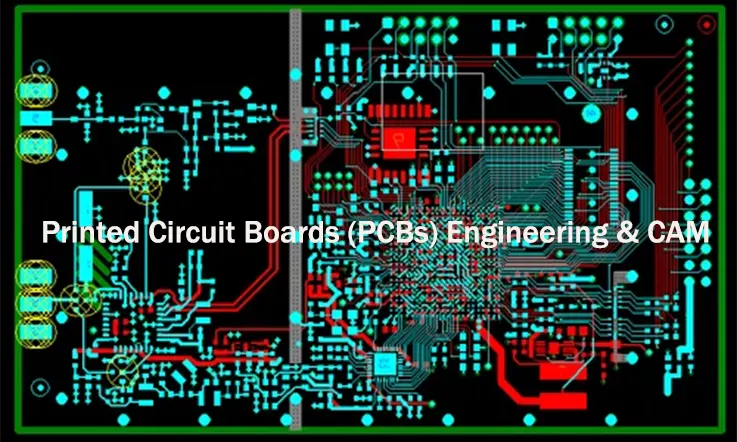
Printed Circuit Board (PCB) engineering and Computer-Aided Manufacturing (CAM) are like the bread and butter of modern electronics production. Every gadget, from smartphones to aerospace control systems, depends on PCBs that are precisely designed and flawlessly manufactured. But here’s the catch—getting a PCB from design to reality isn’t just about placing components on a board. The process demands a seamless transition between PCB engineering and PCB CAM to avoid costly errors, manufacturing delays, and functional mishaps.
In addition, as electronic devices become more advanced, PCB engineering faces increasing demands in signal integrity, power efficiency, thermal management, and miniaturization. From high-density interconnect (HDI) PCBs to multi-layer stack-ups, modern designs require precise layout techniques, optimized routing, and manufacturable structures. This is where PCB CAM (Computer-Aided Manufacturing) software steps in, bridging the gap between ECAD design and fabrication processes.
In this guide, we’re diving deep into how PCBs engineering and PCB CAM work together, breaking down industry best practices, advanced techniques, and how the right software tools can save you from pulling your hair out.
Introduction to PCBs Engineering and PCB CAM
Designing and manufacturing printed circuit boards isn’t just about connecting components and sending them off to production. Every choice in PCB layout, material selection, trace routing, and stack-up configuration affects the performance, reliability, and cost of the final product. But even the most carefully designed board can run into issues if it isn’t optimized for fabrication and assembly.
That’s where PCB CAM (Computer-Aided Manufacturing) steps in. By refining Gerber file processing, CAM tooling adjustments, and DFM/DFT/DFA analysis, PCB CAM ensures that a design is ready for production without last-minute surprises.
This section dives into PCB engineering fundamentals, the role of PCB CAM in manufacturing, and how automation is reshaping the industry. Engineers refining a design and manufacturers aiming to reduce errors must understand these processes to achieve the best results.
What is PCBs Engineering?
The world of PCB engineering revolves around more than just drawing circuit connections. Every PCB must be designed with electrical performance, manufacturability, and long-term reliability in mind. A board that looks great on-screen might be a nightmare to produce if it ignores real-world constraints.
Core Aspects of PCB Engineering-
A well-planned PCB starts with a solid understanding of these elements:
●PCB Layout – Arranging traces, vias, and components in a way that supports signal integrity and power distribution.
●PCB Stack-Up – Choosing the right number and arrangement of layers to balance performance and cost.
●Trace Routing – Determining the best way to connect components while reducing interference.
●High-Speed PCB Design – Managing signal integrity for fast data transmission in applications like RF, DDR, and PCIe circuits.
●Fabrication Process – Understanding how different materials, etching methods, and via structures affect the manufacturability of the PCB.
Industry Applications of PCBs Engineering-
Different sectors require unique PCB engineering approaches:
●Automotive Electronics – Modern vehicles use multi-layer PCBs for safety, infotainment, and power management.
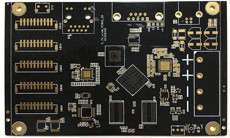
●Consumer Devices – Smartphones, laptops, and smart home products demand high-density, lightweight PCB designs.
●Medical Equipment – Life-saving devices depend on strict signal integrity and low electromagnetic interference (EMI).
●Aerospace & Defense – Harsh environments require ruggedized, high-reliability PCB designs that withstand extreme conditions.
Note: If you’re designing PCBs, ignoring real-world constraints is a shortcut to failure. Material selection, signal integrity, and manufacturing limitations all play a huge role in getting a product to market successfully.
Understanding PCB CAM and Its Role in Manufacturing Optimization
Once a PCB design is finalized, it needs to be translated into machine-readable instructions for fabrication, assembly, and testing. This is where PCB CAM software becomes a necessity. It bridges the gap between design and production, ensuring that everything aligns with factory capabilities.
How PCB CAM Converts a Design into a Manufacturable Product-
PCB CAM tools take the original design files and apply a series of automated checks and adjustments to prepare them for production. This process includes:
●Gerber File Processing – Converting PCB layouts into a format that fabrication machines can read.
●DFM (Design for Manufacturing) Checks – Identifying clearance issues, minimum trace widths, and material limitations.
●DFA (Design for Assembly) Validation – Ensuring that components are positioned for automated assembly without defects.
●DFT (Design for Testability) Enhancements – Adding test points and features that make post-production verification easier.
●CAM Tooling Adjustments – Fine-tuning solder mask layers, silkscreens, and panel layouts for efficiency.
Skipping PCB CAM processing can lead to unforeseen fabrication errors, component misalignment, and wasted material—all of which translate to higher costs and delays.
The Impact of CAM Optimization on Manufacturing Efficiency-
Well-optimized CAM files allow manufacturers to:
●Reduce scrap rates by eliminating design-related issues before fabrication.
●Improve yield by ensuring panelization layouts maximize material usage.
●Speed up production by minimizing last-minute engineering revisions.
Investing time in DFM/DFA/DFT analysis during the PCB CAM stage prevents costly surprises later. Catching problems early means fewer delays, lower costs, and a more predictable production timeline.
The Evolution of PCB CAM and Modern Trends in PCB Engineering
Gone are the days when PCB CAM involved manual file adjustments and trial-and-error corrections. Today, automation and AI-driven analysis have reshaped how designs are prepared for manufacturing.
Advancements in Automated PCB CAM Processing-
Modern PCB CAM software has taken a huge leap forward with AI-assisted verification, predictive analysis, and real-time design adjustments. Instead of we manually reviewing every layer and trace, machine learning algorithms now detect potential production bottlenecks before they happen.
This automation speeds up the process while reducing human errors, making it possible to optimize stack-up designs, drill hole placements, and solder mask definitions with minimal manual intervention.
Cloud-Based PCB CAM and Collaborative Manufacturing-
With more design and manufacturing teams spread across different locations, cloud-based PCB CAM tools allow engineers, PCB fabricators, and assemblers to collaborate in real time. This eliminates the need for constant file exchanges and version mismatches, streamlining the entire workflow.
We can flag a trace width issue or silkscreen misalignment, and our designer can fix it instantly—no back-and-forth emails required. This kind of real-time collaboration minimizes revision cycles and keeps production on schedule.
AI-Driven PCB Engineering and Smart Manufacturing-
Artificial intelligence isn’t just making PCB CAM faster—it’s making it smarter. AI-powered tools can:
●Predict signal integrity issues before prototyping.
●Optimize trace routing for lower EMI and better thermal management.
●Suggest panelization layouts that improve material efficiency.
Essential PCB CAM Processes in PCBs Engineering
The journey from a PCB design concept to a fully fabricated board isn’t just about drawing traces and dropping components on a layout. Without proper CAM processing, even the best designs can run into manufacturing roadblocks, leading to production setbacks and unnecessary costs.
This is why PCB CAM processes play a huge role in bridging the gap between design and fabrication. CAM software ensures that every design is not just functional on screen but also manufacturable on the factory floor.
From preparing design files to optimizing layouts for fabrication and automating error detection, let’s dive into what makes PCB CAM a must-have in modern electronics manufacturing.
Preparing PCB Design Files for CAM Processing
Before a PCB design can move to fabrication, it needs to be translated into a format that PCB manufacturers can understand. PCB CAM software acts as the interpreter, converting complex designs into precise fabrication instructions.
Choosing the Right File Format for Manufacturing-
PCB designs are typically handed off in a few standard file formats, each catering to specific fabrication needs.
| File Format | Purpose | Advantages |
| Gerber (RS-274X) | Defines PCB layers (copper, solder mask, silkscreen) | Industry standard, widely supported |
| ODB++ | Consolidates fabrication, assembly, and testing data | Comprehensive, reduces file misinterpretation |
| IPC-2581 | Vendor-independent format for design-to-fabrication integration | Standardized for modern PCB production |
| Netlist Files | Ensures circuit connectivity correctness | Prevents fabrication mismatches |
●Gerber Files (RS-274X) – The industry standard for defining PCB layers, including copper, solder mask, and silkscreen layers.
●ODB++ – A comprehensive format that consolidates fabrication, assembly, and testing data into a single package.
●IPC-2581 – A neutral, vendor-independent format designed for seamless integration across different manufacturing environments.
●Netlist Files – Ensures that the fabricated PCB matches the original circuit connections.
Sending incomplete or improperly formatted files to a circuit boards manufacturer can cause delays, misinterpretations, or even faulty production runs. That’s why CAM engineers run verification checks before fabrication begins.
Netlist Verification: Catching Hidden Errors Before Production-
A PCB layout might look fine, but unseen errors can cause massive headaches if they aren’t caught early. Netlist verification compares the PCB layout against the original circuit design to ensure:
●No missing connections that could cause open circuits.
●No unintended shorts between traces or components.
●Proper alignment of copper layers to prevent mismatches in multilayer PCBs.
| Potential Issue | Impact on PCB |
| Missing connections | Causes open circuits, rendering PCB non-functional |
| Unintended shorts | Leads to electrical failures and component damage |
| Misaligned copper layers | Creates mismatches in multilayer PCBs |
Skipping this step could mean discovering issues only after production, turning what should have been a seamless build into an expensive rework job.
Panelization Techniques: Making Manufacturing Efficient-
Once the PCB design is validated, the next step is panelization—the process of arranging multiple PCB units onto a single panel for fabrication. Proper panelization ensures:
●Efficient use of materials, reducing waste and lowering costs.
●Easier handling during assembly, minimizing production errors.
●Simplified depaneling, preventing mechanical stress on individual boards.
| Panelization Benefit | Outcome |
| Efficient material usage | Reduces waste and lowers costs |
| Easier handling during assembly | Minimizes production errors |
| Simplified depaneling | Prevents mechanical stress on individual boards |
Ignoring panelization best practices could lead to warped PCBs, alignment issues, and excessive material waste.
Heads-up: Not all manufacturers support every file format, so always check fabrication guidelines before sending your design files.
How PCB CAM Optimizes Design for Manufacturability?
Even if a PCB is perfectly designed, it doesn’t always mean it’s easy to manufacture. PCB CAM software ensures that designs are not just electrically sound but also optimized for fabrication and assembly.
DFM Checks: Preventing Costly Production Mistakes-
PCB CAM software automatically scans designs for potential manufacturing problems, including:
●Trace Width & Spacing Issues – Ensuring traces meet minimum fabrication tolerances to avoid short circuits or etching errors.
●Annular Ring Size – Making sure vias have sufficient copper around drill holes for reliable connections.
●Drill-to-Copper Clearance – Preventing shorts by maintaining safe spacing between drill holes and copper features.
●Solder Mask Expansion – Adjusting mask openings to prevent bridging between pads and traces.
| DFM Check | Purpose | Potential Issue if Ignored |
| Trace Width & Spacing | Ensures fabrication tolerances | Short circuits, etching errors |
| Annular Ring Size | Ensures proper copper around vias | Connection failures, weak vias |
| Drill-to-Copper Clearance | Prevents shorts near drill holes | Electrical failures |
| Solder Mask Expansion | Avoids unintended bridging | Solder bridging, shorts |
Addressing these issues upfront reduces scrap rates, prevents delays, and saves money on production runs.
DFA Considerations: Ensuring a Smooth Assembly Process-
Even if a PCB is perfectly fabricated, poor assembly planning can turn production into a nightmare. CAM software runs DFA (Design for Assembly) checks to make sure:
●Components are properly spaced to accommodate automated pick-and-place machines.
●Silkscreen labels are readable after assembly, avoiding confusion during manual inspections.
●Solder pad sizes are optimized for proper wetting, reducing the risk of cold joints.
| DFA Check | Reason |
| Component spacing | Allows room for automated pick-and-place machines |
| Silkscreen readability | Prevents confusion during manual inspections |
| Solder pad size optimization | Ensures proper wetting, reducing cold joints |
If these issues aren’t caught early, they could lead to assembly defects, increased labor costs, and unnecessary rework.
PCB CAM Automation: Reducing Errors and Enhancing Production Yield
Gone are the days of manual CAM reviews—today’s many PCB fabrication houses use advanced automation tools to detect errors and fine-tune designs for better production results.
How Automated DFM Tools Improve Manufacturing Readiness-
Modern CAM software applies automated DFM rule sets to detect common issues instantly. These automated checks help with:
●Ensuring via drill sizes are within PCB manufacturer tolerances.
●Detecting silkscreen overlaps that could cause confusion in assembly.
●Balancing copper distribution to prevent PCB warping.
| Automated Check | Key Improvement |
| Via drill size verification | Ensures manufacturability |
| Silkscreen overlap detection | Prevents component misidentification |
| Copper balancing | Reduces PCB warping |
By automating these checks, we can reduce human error, improve fabrication accuracy, and accelerate production timelines.
The Role of CAM Rule Sets in Maintaining Quality-
PCB fabs develop custom CAM rule sets tailored to their equipment and processes. These rules ensure:
●Minimum trace widths and spacings are met for a given etching process.
●Drill hole tolerances align with plating and routing capabilities.
●Stencil aperture adjustments optimize solder paste deposition.
| CAM Rule | Quality Improvement |
| Minimum trace widths and spacings | Prevents etching defects |
| Drill hole tolerances | Ensures proper plating and routing |
| Stencil aperture adjustments | Optimizes solder paste deposition |
Failing to adhere to these guidelines can lead to fabrication defects, costly rework, and yield loss.
Boosting Production Yield Through Smart CAM Adjustments-
Every PCB manufacturer aims to maximize yield—getting the highest number of fully functional boards from a production batch. PCB CAM tools help improve yield by:
●Refining solder mask clearances to prevent unintended shorts.
●Optimizing stencil designs to ensure consistent solder paste application.
●Adjusting copper balancing to reduce thermal and mechanical stress.
| Optimization | Yield Improvement |
| Refining solder mask clearances | Prevents unintended shorts |
| Optimizing stencil designs | Ensures consistent solder paste application |
| Adjusting copper balancing | Reduces thermal and mechanical stress |
By integrating these automated processes, PCB CAM significantly enhances production efficiency while maintaining high-quality standards.
Advanced PCB Stack-Up Design and Signal Integrity in PCBs Engineering
In PCB design, setting up the right stack-up configuration, maintaining signal quality, and managing heat effectively help achieve reliable performance. For designs like multi-layer boards and high-speed circuits, these aspects require even more attention, as each layer and its interactions affect overall functionality. We must carefully plan each layer’s design to prevent potential performance issues.
This section will focus on the specific processes and considerations in PCB CAM that help achieve optimal signal integrity and thermal performance, reducing potential design flaws and maximizing the operational efficiency of the final PCB product.
PCB CAM Considerations for Multi-Layer and High-Speed PCB Stack-Ups
Multi-layer PCBs are essential when dealing with complex designs and high-density circuits, but they bring about challenges in signal transmission and thermal management. In these designs, PCB CAM tools assist by validating factors like impedance control, trace width, and material selection.
Controlled Impedance and Dielectric Materials-
In high-speed circuits, maintaining controlled impedance is essential to prevent signal degradation. PCB CAM tools ensure that traces are routed according to impedance rules that help maintain signal quality, particularly in high-frequency designs.
●Dielectric materials influence signal propagation velocity. PCB CAM software can analyze design requirements and recommend suitable materials, assisting our engineers in selecting the most appropriate option for each application.
●Trace width and spacing affect impedance consistency. By verifying that traces adhere to specified width parameters, PCB CAM tools support precise signal transmission and minimize signal reflection.
Trace Width Calculations and Multi-Layer Routing-
Correct trace width is more than just fitting within the available space—it’s about ensuring that signals can travel without causing interference.
●PCB CAM tools allow engineers to run simulations for trace width to ensure that each design specification is met. This includes the careful routing of traces across multiple layers to avoid noise and interference between signal paths.
●Multi-layer routing in high-speed designs requires precision in terms of both trace width and layer allocation, preventing cross-talk and signal coupling.
Proper planning and use of PCB CAM software streamline the routing process, ensuring minimal distortion across the design.
Power and Ground Layer Optimization-
Power and ground planes help maintain voltage stability and reduce electromagnetic interference (EMI). PCB CAM tools provide:
●Ground plane optimization to ensure continuous coverage, which helps reduce signal noise and improves signal quality.
●Power plane design to maintain stable voltage levels across the board.
Correctly designed power and ground layers help in reducing noise and ensuring that the power distribution network (PDN) operates effectively throughout the design.
Signal Integrity and Power Integrity Optimization Through PCB CAM
Signal integrity and power integrity are major considerations for high-speed designs, ensuring that signals travel through the PCB without degradation and power is delivered efficiently to the components.
Minimizing EMI and Crosstalk-
Electromagnetic interference (EMI) can lead to signal distortion and operational instability in high-speed PCBs. PCB CAM tools address this by:
●Ensuring proper trace separation to minimize crosstalk between traces, especially when dealing with sensitive signals.
●Optimizing return paths and integrating shielding around sensitive areas to protect against external EMI.
These optimizations are automated in PCB CAM tools, ensuring that designs meet stringent EMI regulations while minimizing potential interference.
Differential Pair Routing and Layout Optimization-
For high-speed differential signals, proper routing is necessary to ensure signals arrive in sync at the receiving end. PCB CAM software automates the routing of differential pairs, ensuring that:
●The traces are matched in length for synchronized signal transmission.
●The spacing between differential pairs is consistent, helping minimize potential noise or signal degradation.
Optimized differential pair routing helps maintain signal fidelity for high-speed applications, such as data transfer in high-performance computing and communication systems.
Power Delivery Optimization-
Ensuring stable and uniform power delivery to components is a challenge in complex PCB designs. Through PCB CAM, we can:
●Simulate IR drop to check for voltage fluctuations across the PCB, ensuring that power integrity is maintained.
●Perform current density analysis to avoid overheating or inefficient power delivery to components.
Efficient power delivery improves overall device performance, preventing component failures due to power inconsistencies.
Thermal Management and PCB CAM Strategies for Heat Dissipation
Managing heat in high-density PCBs is necessary, especially for high-power circuits. Without proper dissipation, excessive heat may cause component damage or reduced performance.
Thermal Vias and Copper Pours for Heat Dissipation-
Thermal vias are an effective solution to help conduct heat away from high-power components. PCB CAM tools help:
●Optimize via placement for maximum heat transfer from sensitive areas.
●Design copper pours for effective thermal distribution across the PCB.
Thermal management is achieved by ensuring heat flows efficiently from the components to the outer layers of the PCB where it can be dissipated.
Using Heat Sinks and Passive Cooling-
For components that generate significant heat, additional measures like heat sinks and thermal pads are employed. PCB CAM can assist in:
●Planning the integration of heat sinks and thermal vias to promote better heat dissipation.
●Ensuring that materials used for heat sinks are compatible with the PCB design for optimal performance.
Heat dissipation is a main factor in ensuring that components remain within operating temperatures.
Material Selection for Thermal Performance-
Choosing the right materials for a PCB impacts not just electrical performance but also thermal dissipation. PCB CAM tools can help us choose materials with higher thermal conductivity, making it easier to dissipate heat and maintain performance in thermal-heavy applications.
Ensuring PCB Quality Control Through PCB CAM Analysis
Every stage of PCB manufacturing comes with potential issues that can impact the final product. Defects not only lead to scrap and wasted resources but can also result in electrical failures and unreliable performance in end-use applications. This is where PCB CAM (Computer-Aided Manufacturing) steps in as a gatekeeper, catching design flaws before they escalate into costly production errors.
More than just a verification tool, PCB CAM acts as an early-warning system that detects issues in design files, optimizes layout for manufacturing, and minimizes errors during fabrication and assembly. The following sections will explore how PCB CAM enhances production efficiency, reduces defect rates, and ensures electrical performance through rigorous testing.
How PCB CAM Enhances Manufacturing Yield and Reduces Defects?
To maintain stable PCB production, minimizing defects is a top priority. Leveraging PCB CAM allows manufacturers to simulate production conditions, spot potential failures, and make corrections before fabrication even begins.
Automated Optical Inspection (AOI) and X-ray Inspection-
Throughout production, AOI (Automated Optical Inspection) quickly identifies missing components, poor solder joints, short circuits, and open traces. Using high-resolution cameras, AOI scans the PCB surface far more efficiently than manual inspection, significantly reducing human error.
For hidden solder joints, such as Ball Grid Array (BGA) components, X-ray inspection becomes essential. It reveals hidden defects like voids, cold solder joints, and misalignments. Integrating AOI and X-ray inspection within PCB CAM creates a closed-loop system where design and production teams can make real-time adjustments to improve overall manufacturing quality.
| Inspection Method | Defects Detected | Best Use Case |
| AOI (Automated Optical Inspection) | Missing components, solder defects, open circuits | Surface-mounted components |
| X-ray Inspection | Hidden solder voids, BGA misalignment, cold joints | Multi-layer PCBs, BGAs |
Solder Joint Analysis and Reflow Profiling-
Solder joint reliability directly impacts PCB longevity. If reflow soldering temperatures are not properly controlled, issues such as cold solder joints, bridging, or incomplete wetting can occur. PCB CAM simulates solder joint behavior and optimizes the reflow temperature curve to ensure proper bonding.
Additionally, PCB CAM evaluates pad design, ensuring that pad sizes match component leads, eliminating pad misalignment issues, and preventing problems like tombstoning or solder paste misplacement.
Panel Optimization to Improve Material Utilization-
For high-volume production, panel layout significantly affects manufacturing costs. Poor panel design wastes substrate material and can lead to mechanical stress issues. PCB CAM applies panelization algorithms to determine the most efficient layout, maximizing the number of PCBs per panel while preventing mechanical failures like board warping or cracking.
Design Rule Check (DRC) in PCB CAM: Preventing Common PCB Errors
Many PCB failures originate from design errors, including inadequate trace widths, via violations, and misaligned solder masks. If these mistakes go unnoticed in the design phase, they can lead to performance degradation, electrical shorts, or manufacturability issues. PCB CAM performs DRC (Design Rule Check) to automatically detect these violations before the design moves to production, saving time and preventing costly rework.
Via and Annular Ring Clearance Checks-
Vias connect different PCB layers, but if poorly designed, they can cause electrical and soldering issues. PCB CAM verifies via size, annular ring clearance, and pad-to-via spacing to ensure robust electrical connections and reliable manufacturing.
| Design Parameter | Optimal Value Range | Potential Issue if Violated |
| Via Diameter | 0.2mm – 0.5mm | Weak electrical connections |
| Annular Ring Width | ≥ 0.1mm | Poor plating adhesion, open circuits |
| Pad-to-Via Clearance | ≥ 0.2mm | Risk of solder bridging, short circuits |
Trace Width, Spacing, and Drill Hole Tolerance Control-
Every PCB trace must adhere to minimum width and spacing guidelines to prevent short circuits and impedance mismatches. PCB CAM measures signal traces, calculates impedance matching, and detects violations to ensure compliance with fabrication tolerances.
Drill hole tolerances also require strict control. If via holes deviate from specified dimensions, they may cause plating failures or lead to mechanical instability. PCB CAM automatically checks drill hole sizes to ensure they remain within acceptable limits.
Solder Mask Alignment Verification-
The solder mask protects PCB surfaces from oxidation and accidental solder bridging. However, if misaligned, exposed copper can create short circuits or lead to corrosion. PCB CAM runs precise solder mask alignment checks, correcting misalignments to maintain circuit reliability over time.
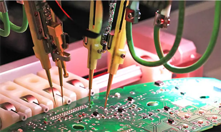
Implementing Electrical Testing (DFT) with PCB CAM for Reliability
Even after a PCB is built according to specifications, verifying its electrical functionality remains necessary. DFT (Design for Testability) ensures each PCB undergoes comprehensive electrical testing before use. PCB CAM helps plan and refine test points, making testing more straightforward and enhancing reliability.
Flying Probe Testing and In-Circuit Testing (ICT)-
Flying Probe Testing is ideal for prototype and low-volume production since it provides flexible, point-by-point electrical testing without requiring a custom fixture. PCB CAM optimizes probe paths to minimize test time while maximizing fault detection.
For high-volume production, In-Circuit Testing (ICT) is the preferred approach. ICT relies on Bed-of-Nails test fixtures, allowing simultaneous testing of multiple circuits. PCB CAM ensures that test points are optimally placed, preventing the risk of untestable connections that could cause functional failures later on.
| Test Method | Best for | Key Advantage | Limitations |
| Flying Probe Testing | Low-volume, prototyping | No fixture required, flexible | Slower than ICT |
| In-Circuit Testing (ICT) | High-volume production | Fast, parallel testing | Requires custom fixture |
Functional Testing and Test Point Optimization-
Beyond basic continuity checks, functional testing examines real-world circuit behavior, such as signal integrity, power consumption, and thermal performance. PCB CAM arranges test point distribution to guarantee access to all essential nodes, allowing functional tests to cover all necessary electrical paths.
How Choosing PCB CAM Software for Efficient PCB Engineering?
Printed circuit board production relies on precise data handling, thorough design verification, and seamless integration between design and fabrication. PCB CAM software acts as the bridge between electronic design automation (EDA) tools and the manufacturing floor, ensuring that layouts are checked for manufacturability, fabrication data is properly formatted, and potential issues are caught before production.
With multiple options available, selecting the right PCB CAM tool depends on its capabilities, compatibility with design software, and how well it supports automated checks and optimization. Understanding how these tools function can help avoid common errors, streamline production, and improve overall workflow efficiency.
Comparing PCB CAM Software: Features and Performance
Different PCB CAM solutions cater to various stages of the fabrication process. Some focus on validating designs, while others provide in-depth panelization and automated manufacturing checks. Below are some widely used options:
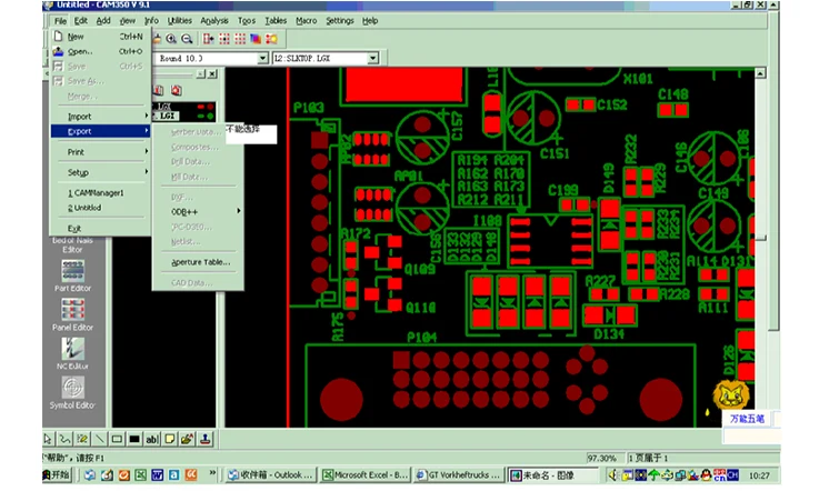
1. CAM350-
A widely used solution that allows engineers to inspect, edit, and verify PCB designs before manufacturing. It includes design rule checks (DRC), panelization tools, and Gerber file editing, making it a preferred choice for preparing boards for fabrication.
2. Altium CAM Editor-
Built into Altium Designer, this tool simplifies the transition from ECAD to CAM by offering native support for Gerber, ODB++, and IPC-2581 formats. It is particularly useful for those already working in the Altium environment.
3. Valor NPI-
Developed by Siemens, this software specializes in automated design-for-manufacturability (DFM) analysis, identifying potential assembly challenges like incorrect component footprints, solder paste misalignment, and electrical testability issues.
4. Genesis and Frontline InCAM-
Both developed by Orbotech (now part of KLA Corporation), these tools are widely adopted by PCB manufacturers. Genesis offers extensive CAM editing and fabrication job preparation, while Frontline InCAM enhances process automation, panel optimization, and manufacturability improvements.
5. Ucamco Integr8tor-
This software is designed to automate PCB data analysis and generate instant manufacturability reports. It is particularly useful for fabricators who need to assess multiple designs quickly without extensive manual input.
Each tool offers a different balance of features, and the right choice depends on project requirements, manufacturing complexity, and how well it integrates into existing workflows.
What to Look for When Choosing PCB CAM Software?
Selecting PCB CAM tools involves considering several factors that impact design verification, fabrication readiness, and overall efficiency. Some of the core areas to evaluate include:
1. Error Detection and Design Verification-
Fabrication defects often stem from design oversights such as trace width violations, solder mask misalignment, and annular ring clearance issues. A robust PCB CAM tool should automatically flag these concerns, preventing costly rework.
2. Integration with ECAD Tools-
For teams using design software like Altium, Cadence, or KiCad, seamless data transfer to CAM software is necessary. Direct compatibility minimizes conversion errors and speeds up manufacturing preparation.
3. Automation and Workflow Optimization-
Modern PCB CAM tools include automation features such as DFM checks, panelization, and test point optimization. These functions reduce manual intervention and accelerate the transition from design to production.
4. File Format Support-
A well-rounded PCB CAM system should support widely used fabrication formats, such as:
●Gerber (RS-274X) – The standard format for PCB manufacturing
●ODB++ – A richer format preferred for seamless data exchange
●IPC-2581 – A modern open-standard format improving industry-wide compatibility
5. Vendor Support and Software Updates-
Manufacturing processes evolve, and having access to software updates and technical support ensures that engineers can keep up with new fabrication requirements and technological advancements.
Integrating PCB CAM Software into PCB Design and Fabrication
Smooth integration between design tools and CAM software eliminates manual errors and speeds up production. The following workflow outlines how PCB CAM tools fit into the overall PCB fabrication process:
1. ECAD to CAM Transition-
After finalizing a PCB layout, the design is exported in a manufacturing-ready format (e.g., Gerber, ODB++, IPC-2581). The CAM software then runs validation checks to ensure the design meets fabrication guidelines.
2. Automated DFM Analysis-
Advanced PCB CAM tools provide real-time feedback, enabling we to resolve manufacturability issues before production begins. This minimizes fabrication delays and avoids unnecessary re-spins.
3. Manufacturing File Preparation-
Once the CAM review is complete, the software generates essential files for production, including:
●NC Drill files for defining hole placements
●Solder paste layers for stencil creation
●Panel layouts to optimize material usage
4. Smart Factory and Process Automation-
Some advanced PCB CAM solutions integrate with smart manufacturing systems, enabling real-time monitoring, predictive analysis, and adaptive process adjustments. This helps improve fabrication efficiency and consistency.
PCB CAM Tooling and Manufacturing Guidelines in PCB Engineering
Manufacturing a PCB requires more than just following a blueprint. Every step, from panelization to solder mask application and material utilization, must be carefully managed to avoid unnecessary costs and production delays. PCB CAM tooling plays a direct role in shaping fabrication efficiency, ensuring smooth transitions between design, assembly, and testing.
A carefully planned CAM processing approach helps eliminate design bottlenecks, reduce material waste, and maintain efficient production timelines. Below are some of the most effective strategies utilized in PCB CAM tooling and manufacturing.
Understanding PCB Panelization and Tooling Optimization in CAM
Panelization allows multiple PCBs to be produced together, making fabrication faster and reducing handling time. The way boards are arranged in a panel affects everything from material usage to assembly precision.
1. Breakaway Tabs and V-Scoring: Choosing the Right Separation Method-
When manufacturing in bulk, individual PCBs need a clean and efficient separation method. Two common techniques are:
●Breakaway Tabs: These small sections of material hold the PCB in place during fabrication. To make them easier to remove, they often feature perforations, sometimes referred to as “mouse bites.”
●V-Scoring: A shallow cut is made along the surface of the PCB, allowing it to snap apart after assembly. This method works well for straight-edged designs and high-volume runs.
| Separation Method | Advantages | Disadvantages |
| Breakaway Tabs | Easy to implement, supports irregular shapes | May leave rough edges, requires more space |
| V-Scoring | Ideal for straight edges, fast removal | Not suitable for complex board shapes |
2. Routing vs. Punching for PCB Separation-
The method used to detach boards from a panel affects speed and material usage.
●Routing: A CNC machine mills out the board shape. This method is flexible but generates more waste.
●Punching: A dedicated press quickly separates PCBs using a pre-made die. This approach is faster but requires upfront tooling investment.
3. Fiducial Marks for Precise SMT Pick-and-Place Alignment-
Fiducial marks act as reference points for automated assembly equipment. Without them, pick-and-place machines may misalign components, especially on dense PCBs. To improve accuracy, these small copper pads should be:
●Placed symmetrically on opposite corners of the board.
●Free from solder mask or silkscreen coverage.
●Consistently sized across all production runs.
4. Panel Layout and Waste Reduction-
Maximizing panel efficiency lowers material costs. By arranging PCBs tightly without unnecessary gaps, we minimize wasted substrate and improve overall yield. Strategic nesting of boards allows for better material utilization.
Solder Mask, Silkscreen, and Copper Layer Considerations in PCB CAM
Fine-tuning solder mask openings, silkscreen placement, and copper balancing prevents defects and enhances durability. These layers do more than just protect the PCB—they influence long-term performance.
1. Solder Mask Openings and PCB Protection-
The solder mask prevents unintended solder bridges, oxidation, and contamination. However, certain areas must remain exposed for proper assembly:
●Component pads must be fully open to allow solder adhesion.
●Clearance between mask openings and copper traces must be carefully set to avoid exposure issues.
●For fine-pitch components, a properly defined mask prevents shorts and alignment errors.
| Solder Mask Design Factor | Impact on PCB Manufacturing | Potential Issue if Ignored |
| Pad Opening Size | Ensures solderability without bridging | Cold joints or solder shorts |
| Clearance from Traces | Prevents unintended copper exposure | Electrical shorts |
| Fine-Pitch Mask Definition | Supports precise component placement | Misalignment and solder issues |
2. Silkscreen Readability and Placement-
Silkscreen markings provide component labels, polarity indicators, and assembly guidance. To avoid issues during production:
●Text should be large enough to remain readable after printing.
●Avoid placing silkscreen on solder pads, which can interfere with soldering.
●Use high-contrast colors for better legibility (e.g., white silkscreen on a green mask).
3. Copper Layer Balancing to Prevent PCB Warping-
Uneven copper distribution leads to mechanical stress during thermal cycling. To avoid board warping and twisting, copper layers must be evenly distributed. Techniques include:
●Adding copper fills in low-density areas to even out material distribution.
●Symmetrically designing inner and outer copper layers to avoid stress imbalances.
4. Surface Finish Selection: HASL, ENIG, and OSP-
The type of surface finish affects solderability, oxidation resistance, and long-term reliability. Common choices include:
●HASL (Hot Air Solder Leveling): Economical but not ideal for fine-pitch components.
●ENIG (Electroless Nickel Immersion Gold): Provides better oxidation resistance and smoother solderability.
●OSP (Organic Solderability Preservative): A cost-effective, lead-free option with a shorter shelf life.
Choosing the right finish depends on assembly requirements, environmental exposure, and storage conditions.
Cost Optimization Strategies in PCB CAM for Large-Scale Manufacturing
Efficient CAM strategies help us reduce material usage, minimize processing time, and eliminate unnecessary expenses. These approaches streamline production while maintaining quality.
1. Maximizing Material Utilization-
The more efficiently a panel is arranged, the less material is wasted. Manufacturers optimize layouts by:
●Minimizing gaps between PCBs to fit as many boards as possible per panel.
●Standardizing board sizes to simplify production planning.
●Using shared tooling strips to reduce cutting waste.
| Optimization Strategy | Material Savings | Impact on Cost |
| Tight PCB Nesting | Reduces unused panel space | Lower material costs |
| Standardized PCB Dimensions | Simplifies panel arrangement | Faster production setup |
| Shared Tooling Strips | Minimizes cutting waste | Less scrap and higher yield |
2. Reducing Drill Costs by Limiting Hole Variations-
Drilling is one of the slowest steps in PCB fabrication. The fewer drill bit changes required, the faster the process. Cost-saving techniques include:
●Standardizing via and hole sizes instead of using many different diameters.
●Avoiding microvias unless necessary, as they require advanced drilling techniques.
3. Cutting Production Waste by Catching Errors Early-
CAM software catches many common design mistakes before fabrication begins, such as:
●Missing solder mask clearances
●Overlapping silkscreen on pads
●Incorrect drill-to-pad alignment
Addressing these errors ahead of time prevents costly rework and material loss.
4. Faster Turnaround with Automated CAM Processing-
Modern CAM software automates design verification, panelization, and manufacturing prep, reducing the time from design submission to production. This speeds up delivery schedules and increases overall efficiency.
5. Large-Scale Batch Processing Efficiency-
For high-volume manufacturing, batch processing saves both time and money. Strategies include:
●Combining multiple small orders into a single production run.
●Standardizing PCB thicknesses to simplify fabrication.
●Pre-optimizing solder mask and paste layers for repeatable consistency.
High-Density Interconnect (HDI) PCBs and PCB CAM Challenges
As electronic devices become more compact and complex, HDI (High-Density Interconnect) PCBs have become a best choose solution for maximizing functionality within limited space. These circuit boards rely on microvias, fine-pitch components, and multi-layer stack-ups, pushing fabrication techniques to their limits.
Unlike standard PCBs, HDI designs demand precision at every stage, from via formation to layer registration. Without CAM-driven verification, manufacturers risk misalignment, material waste, and inconsistent electrical performance.
Let’s explore how PCB CAM ensures smooth HDI fabrication, covering design preparation, manufacturing accuracy, and cost-efficient strategies.
Why HDI PCBs Require Advanced PCB CAM Techniques?
HDI designs challenge traditional fabrication methods, requiring laser-drilled vias, sequential lamination, and controlled layer stack-ups. Proper CAM processing prevents costly mistakes that could disrupt production.
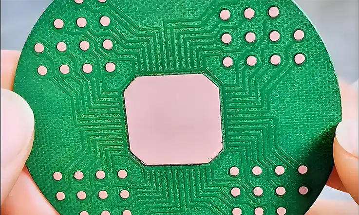
1. Microvia Design and Via-in-Pad Implementation-
Unlike mechanically drilled vias, microvias are laser-drilled and must be carefully positioned to maintain electrical performance and structural reliability. PCB CAM plays a role in:
●Ensuring microvia alignment across multiple layers.
●Checking aspect ratio limitations to prevent reliability issues.
●Optimizing via-in-pad structures to support high-speed signals without unwanted electrical interference.
2. Sequential Lamination and HDI Layer Stack-Up-
HDI PCBs rely on sequential lamination, where multiple fabrication steps increase the chance of misalignment, resin starvation, and warping. PCB CAM reduces these risks by:
●Simulating layer compression effects before production.
●Verifying drill-to-copper spacing to maintain electrical clearance.
●Automating impedance calculations to meet signal integrity requirements.
3. Fine-Pitch Component Placement and Routing Adjustments-
With BGA (Ball Grid Array) and CSP (Chip Scale Package) components shrinking to 0.4mm pitch and below, routing traces between pads requires careful planning. PCB CAM enhances this process by:
●Applying automated fan-out routing to escape dense pin grids.
●Adjusting trace width-to-space ratios based on fabrication tolerances.
●Generating high-resolution manufacturing plots to prevent etching defects.
Overcoming Manufacturing Challenges of HDI PCBs with PCB CAM
HDI fabrication introduces challenges that extend beyond standard PCB manufacturing, from laser drilling precision to impedance-controlled routing. Addressing these factors through CAM-driven analysis and verification leads to more consistent results.
1. Laser Drilling Accuracy for Microvias-
HDI PCBs require laser-drilled microvias that must align precisely with inner copper layers. PCB CAM enhances accuracy by:
●Generating optimized drill coordinates to prevent breakouts.
●Applying correct laser ablation settings to avoid over-etching.
●Verifying stacking rules to avoid structural weaknesses.
2. Via-in-Pad Technology and Planarization Considerations-
Via-in-pad structures improve signal transmission but require planarization techniques to avoid assembly defects such as solder voids and uneven surfaces. PCB CAM helps by:
●Defining appropriate solder mask clearances to prevent solder wicking.
●Recommending resin fill or copper cap methods for a smooth finish.
●Simulating thermal expansion effects to prevent layer delamination.
3. High-Aspect Ratio Vias and Plating Control-
High-aspect ratio vias (depth-to-diameter ratio >10:1) require precise plating techniques to ensure electrical continuity without mechanical stress. CAM-driven plating analysis assists by:
●Calculating copper thickness requirements for consistent conductivity.
●Optimizing drill parameters to prevent hole breakage.
●Predicting plating uniformity issues before fabrication starts.
4. Impedance-Controlled Routing and Signal Integrity Preservation-
HDI PCBs carry high-speed signals, making impedance consistency a priority. CAM software assists by:
●Adjusting trace width and spacing based on dielectric constants.
●Adding controlled impedance test structures for validation.
●Preventing signal degradation through automated checks.
5. Registration Precision for Layer-to-Layer Alignment-
As HDI stack-ups grow in complexity, misalignment between layers can result in shorts, open circuits, or fabrication scrap. PCB CAM reduces these risks by:
●Providing fiducial alignment analysis for precise layer registration.
●Simulating shrinkage and expansion effects during lamination.
●Applying dynamic adjustments to compensate for potential material distortion.
PCB CAM Strategies for Reducing Cost and Complexity in HDI PCB Production
HDI PCBs increase fabrication expenses due to specialized materials, advanced drilling techniques, and additional process steps. CAM-driven solutions help optimize manufacturing efficiency while maintaining product performance.
1. Optimizing Panel Utilization to Reduce Material Waste-
HDI PCBs often require custom panel layouts, but inefficient planning leads to higher material waste. CAM software assists in:
●Nestling smaller boards together to improve material efficiency.
●Minimizing border clearances while maintaining fabrication tolerances.
●Predicting material shrinkage to avoid misaligned cuts.
2. Staggered vs. Stacked Vias: Finding the Right Balance-
Stacked vias provide compact routing, but staggered vias offer better reliability at lower costs. CAM processing helps us:
●Compare trade-offs between staggered and stacked configurations.
●Apply optimized drill sequencing to reduce via collapse risks.
●Balance via structures to prevent stress buildup.
3. Choosing the Right Substrate Material for Cost-Effective Performance-
Material selection affects HDI production expenses and electrical properties. PCB CAM ensures compatibility by:
●Simulating dielectric loss and signal speed effects across different materials.
●Matching material properties with design requirements.
●Optimizing thermal expansion coefficients to prevent delamination.
4. CAM-Driven Yield Improvements to Minimize Scrap Rates-
Defective HDI PCBs increase production costs due to scrap rates and rework expenses. CAM automation reduces these issues by:
●Detecting common fabrication errors before production begins.
●Providing predictive failure analysis to flag potential defects.
●Generating precision manufacturing files for improved first-pass yield rates.