
This document offers a practical examination of the ITEQ IT-150GS laminate system, viewed entirely through the lens of high-yield printed circuit board production. Moving beyond the static figures of a datasheet, this analysis explores the material’s authentic behavior within the demanding environment of advanced electronics—from high-speed digital and HDI structures to the unforgiving requirements of AI, EV, and 5G hardware. The insights that follow are intended to empower engineers and production leaders to build multilayer boards that are not merely reliable and manufacturable, but also economically sound. This is a narrative about transforming a raw material into the functioning, reliable heart of modern technology.
Unpacking the Core Attributes of IT-150GS Material
The utility of ITEQ IT-150GS arises from a thoughtfully engineered equilibrium of its properties. This balance is something to be understood and leveraged within a production setting, as it provides the wide and forgiving process window needed for intricate production sequences. This understanding fosters predictable results and instills a high degree of confidence in the long-term field performance of the electronic assemblies produced from it.
Thermal Stability and Mechanical Resilience Under Stress
The intense thermal events of multilayer lamination and component assembly are where a material’s true character is tested. Its ability to remain dimensionally and structurally stable under such duress is a direct determinant of production yields and its ultimate service life. A PCB circuit board fabricator’s skill lies in using this stability to its full advantage.
Glass Transition Temperature (Tg ~155°C):
This thermal threshold is not just a number; it is the operational headroom provided for modern lead-free soldering. This property is capitalized upon to subject boards to multiple, high-temperature reflow profiles, with peaks reaching 260°C, without inducing plastic deformation. This preserves the board’s structural integrity throughout the complex assembly journey.
Decomposition Temperature (Td ~365°C):
A high decomposition temperature points to a robust chemical architecture. In a production environment, this translates into a substantial margin of safety. It means the material can withstand the brief but intense heat of soldering without degrading or losing significant mass, allowing for more aggressive or complex assembly without risking the laminate’s integrity.
Delamination Resistance:
The laminate’s endurance is best quantified by its performance in thermal stress testing. With a time-to-delamination at 260°C (T260) and 288°C (T288) both exceeding 60 minutes, it demonstrates a profound resilience. This allows for complex rework operations or the assembly of high-thermal-mass components with confidence that the board will not delaminate under localized thermal shock.
Dimensional Fidelity:
The low Z-axis Coefficient of Thermal Expansion (CTE) of IT-150GS, a product of its refined resin and filler formulation, is a property to be managed. During production, this minimizes the expansion and contraction stress exerted on plated through-hole (PTH) barrels during thermal cycling. By controlling for this, the final reliability of vias in high-layer-count boards is greatly enhanced, preventing latent field failures.
Warpage Mitigation:
The low-stress nature of IT-150GS can be used to produce exceptionally flat boards. By advising on symmetrical stackups and implementing balanced copper distribution, a production facility can counteract the natural tendency for boards to warp, even in high-layer-count builds. The result is a surface held to a high standard of planarity, a prerequisite for precision component placement in modern SMT lines.
Table: Key Thermal and Mechanical Performance Metrics:
| Property | Value / Performance |
| Glass Transition Temperature (Tg) | ~155°C |
| Decomposition Temperature (Td) | ~365°C |
| Time-to-Delamination @ 260°C | >60 minutes |
| Time-to-Delamination @ 288°C | >60 minutes |
| Z-Axis CTE | Low |
| Warpage Tendency | Very Low (with symmetrical stackup) |
Electrical Performance and Signal Integrity Benchmarks
For circuits operating at elevated frequencies, steadfast electrical behavior is the desired outcome. The job of the production process is to translate the material’s inherent properties into guaranteed performance.
Dielectric Constant (Dk):
The well-defined Dk value of IT-150GS (around 4.0 to 4.2 at 1-2 GHz) is used as a reliable input for impedance modeling. This allows design and production teams to accurately calculate and then physically produce transmission lines to precise targets, like 50Ω single-ended or 100Ω differential pairs, with a high degree of fidelity.
Dissipation Factor (Df):
The low dissipation factor of this material (approximately 0.010 at 1-2 GHz) signifies minimal signal energy absorption. A knowledgeable manufacturer leverages this by fabricating high-speed channels that preserve signal amplitude and shape over moderate trace lengths, directly enabling applications like PCIe 4.0 to function with lower bit-error rates.
Conductive Anodic Filament (CAF) Resistance:
The inherent resistance to electrochemical migration in IT-150GS provides a distinct production advantage. It allows for the confident creation of boards with more aggressive design rules, such as tighter via-to-via spacing, which in turn enables clients to achieve greater product miniaturization without sacrificing long-term operational integrity in humid or high-temperature environments.
Table: Electrical Signal Integrity Parameters:
| Electrical Property | Measured Value | Relevance to Design |
| Dielectric Constant (Dk) | ~4.0–4.2 @ 1–2 GHz | Enables accurate impedance control for high-speed traces |
| Dissipation Factor (Df) | ~0.010 @ 1–2 GHz | Low loss supports PCIe, DDR, and SerDes signaling |
| CAF Resistance | High | Prevents failure in high-density, humid environments |
| Impedance Control Capability | 50Ω (SE) / 100Ω (Diff) achievable | High accuracy for RF and high-speed digital boards |
Halogen-Free Chemistry and Global Compliance
A fabricator serves as a client’s gateway to the global market. The choice of material and the ability to process it correctly are deeply connected to regulatory acceptance.
Halogen-Free Formulation:
By expertly processing a material that achieves its UL 94 V-0 flame retardancy without bromine or chlorine compounds, PCB Manufacturer (JarnisTech) helps its clients meet the growing demand for greener electronics. This adherence to standards like IEC 61249-2-21 simplifies the client’s supply chain compliance.
Global Market Access:
Utilizing a material that is fully compliant with the European Union’s RoHS and REACH directives means a board house can deliver products that face no regulatory barriers to entry in markets worldwide. This service streamlines the documentation and validation process for a client’s international product launches.
Low Moisture Absorption:
The material’s low moisture absorption rate (<0.12%) is a process benefit. A controlled-humidity production environment, combined with this property, dramatically reduces the risk of delamination or “popcorning” during reflow soldering. This manufacturing discipline translates directly into higher yields and more reliable final products for the customer.
Chemical Resistance:
A thorough understanding of the material’s resilience to various chemical baths in the DES process is required. Proper handling ensures that the integrity of fine-line circuitry and the board surface is protected from degradation, a mark of a quality-focused manufacturing operation.
Table: Environmental and Regulatory Properties:
| Property / Standard | Value / Compliance |
| Halogen Content | Halogen-free (per IEC 61249-2-21) |
| Flame Retardancy | UL 94 V-0 without Br/Cl |
| RoHS/REACH Compliance | Fully Compliant |
| Moisture Absorption Rate | <0.12% |
| Chemical Resistance | High (suitable for DES process chemicals) |
The Art of Fabrication: Our Process for Maximizing IT-150GS Potential
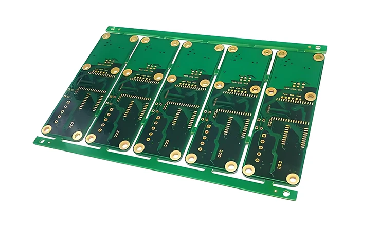
A superior laminate is merely a starting point; it is the mastery of the production process that transforms its potential into a tangible, reliable product. Deep familiarity with IT-150GS allows for the harnessing of its strengths through precisely controlled production disciplines.
●Fabricator’s Note on Design for Manufacturability (DFM): It is not uncommon to receive designs with non-symmetrical stackups or imbalanced copper distribution. While these are often technically possible to produce, they present a higher risk of bow and twist after lamination, which can complicate assembly and affect long-term reliability. A pre-production engineering review proactively identifies these potential issues. The engineering team then collaborates with the client’s designers, providing alternative layup options that balance electrical performance with optimal manufacturability. This collaborative DFM approach is fundamental to preventing yield issues and ensuring a smoother path from design to final product.
Seamless Process Integration with Standard FR-4 Workflows
A considerable production advantage of IT-150GS lies in its direct compatibility with well-established FR-4 process flows. This allows a board house to deliver performance enhancements to its clients without the cost and delay of extensive process re-engineering.
●Standard Lamination Cycles: The material’s resin flow and cure profile align perfectly with standard press cycles optimized for 6- to 16-layer boards. This means a full, reliable cure can be achieved without special handling or extended press times, leading to efficient and cost-effective production for the client.
●Predictable Registration: Throughout the sequential lamination steps of a multilayer build, the material maintains its dimensional stability. Skilled execution translates this predictability into highly accurate layer-to-layer registration, a necessity for achieving reliable interconnects in today’s dense designs.
●Clean Imaging Results:The laminate surface responds well to standard dry film photoresist lamination and exposure. A controlled process yields sharp, well-defined trace edges after development—the first physical step toward creating circuits with accurate impedance for the end application.
●Oxide Bonding Integrity: The process of creating a dependable, high-adhesion bond with oxide or oxide-alternative treatments is a craft. A strong bond ensures robust interlayer adhesion, preventing failures under thermal or mechanical stress and delivering a more durable product to the customer.
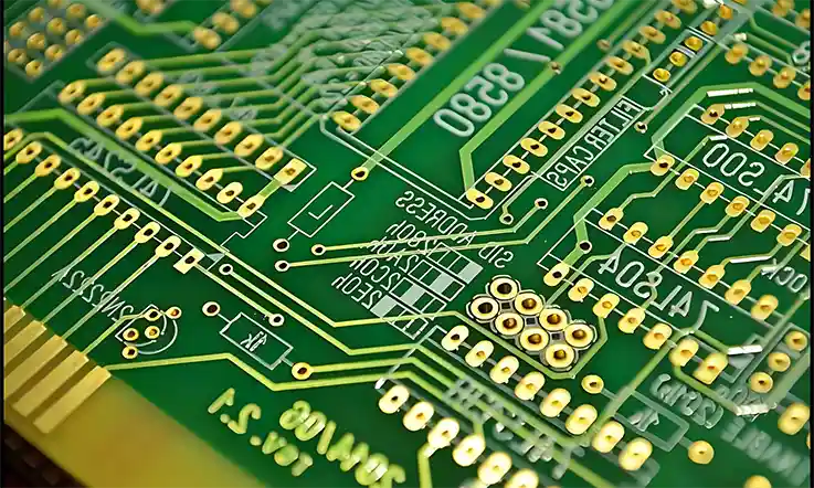
Precision Drilling and Achieving Superior Hole-Wall Integrity
In designs featuring high layer counts or fine-pitch BGAs, the quality of the drilled hole is a direct predictor of final product reliability. The drilling process must be tailored to the specific mechanical behavior of IT-150GS.
●Minimal Smear Formation: By employing carefully selected drill bits and optimized feed/speed rates, the material’s tough resin system allows for the creation of clean hole walls with minimal resin smear. This simplifies the subsequent desmear process and ensures a pristine copper surface is available for plating, a foundational step for via reliability.
●Superior Hole-Wall Quality: The outcome of clean drilling is a smooth, uniform hole wall. This surface enables even deposition during the electroless copper process, creating a conductive foundation that promotes a strong, void-free electrolytic copper plating. This attention to detail in the early stages prevents future open circuits.
●High-Density Drilling: The ability to drill mechanical microvias as small as 0.15mm (6 mils) without causing excessive debris or resin pull-out demonstrates a mastery of the material and machinery, directly enabling clients’ high-density interconnect (HDI) designs.
●Verified Plating Reliability: The integrity of the plated vias is confirmed through Interconnect Stress Testing (IST), where coupons undergo hundreds of thermal cycles to simulate a lifetime of use. Unwavering low-resistance readings from these tests provide tangible proof of excellent copper adhesion and barrel integrity in the finished boards.
Advanced Lamination Strategies for Warpage Control
A flat board is a manufacturable board, and achieving planarity is a science. The combination of IT-150GS’s inherent stability and disciplined process control delivers exceptional results.
●Optimized Press Profiles: Precisely staged temperature ramps and pressure profiles are utilized during lamination. This technique ensures the epoxy resin achieves a full, uniform cure while minimizing the introduction of internal stresses that can lead to warpage in the final product.
●Symmetrical Design Philosophy: Experienced production teams (JarnisTech) often collaborate with clients during the design phase to encourage symmetrical stackups and balanced copper distribution. When these design principles are paired with IT-150GS in a controlled lamination process, the result is a board with outstanding flatness, often achieving warpage of less than 0.7% on large 18” x 24” panels.
●High-Match Prepreg System:Pairing IT-150GS cores with their corresponding IT-150GS prepreg (PP) is standard practice. Knowledge of this system’s controlled resin flow characteristics allows for the effective filling of dense copper patterns without causing resin starvation in sparse areas. This guarantees foreseeable final dielectric thicknesses, which is fundamental for impedance control.
Ensuring Solderability and Lead-Free Assembly Success
The final test of a board’s manufacturability happens at the client’s assembly line. All prior production work is aimed at ensuring this stage is successful.
●High-Temperature Endurance:Boards built on IT-150GS are fully compatible with lead-free reflow profiles peaking at 260°C, showing no evidence of delamination even after multiple passes.
●Robust Thermal Margins: The material’s high Td and excellent T260/T288 performance, when processed correctly, result in a board with a wide process window. This allows the client to perform complex assemblies that may require double-sided reflow or rework with a much lower risk of board failure.
●Broad Surface Finish Compatibility: The application of advanced surface finishes like ENIG, OSP, or Immersion Silver on the IT-150GS surface ensures superior solder wetting and reliable joint formation for the client’s components.
High-Speed and High-Frequency Performance Analysis
Achieving signal integrity in high-frequency domains is an exercise in precision. It requires transforming a laminate’s dependable dielectric properties into guaranteed circuit performance through an expertly engineered fabrication process.
Achieving Precise Impedance Matching for GHz Signals
Controlling impedance at high frequencies is a function of both material science and exacting process control. For designs built on IT-150GS, the focus is on the following to ensure impedance accuracy.
●Dielectric Foundation: The material’s dielectric constant serves as a predictable baseline for impedance calculations across all layers of the PCB stackup.
●Geometrical Precision: By combining Statistical Process Control (SPC) on etching lines with TDR verification, our engineers delivers impedance control within a tight ±5% tolerance, often achieving ±3% on sensitive differential pairs.
●Layer-to-Layer Spacing Control: Through meticulously managed lamination cycles, the designed dielectric spacing is preserved, a requirement for predictable transmission line performance above 10 GHz.
●Process Validation: Final impedance is verified with Time Domain Reflectometry (TDR) measurements performed on test coupons produced with every panel, confirming adherence to design specifications for the client.
Understanding Loss Tangent in High-Speed Digital Routing
Minimizing signal loss is a collaborative effort between designer and fabricator, managed by leveraging the material’s properties and optimizing every manufacturing step that influences attenuation.
●Low-Loss Material Profile: The dissipation factor of IT-150GS allows for the successful fabrication of high-speed digital designs like PCIe 4.0 or 20Gbps SerDes over moderate trace lengths.
●Copper Surface Roughness Control: Copper surface profiles can be managed during pre-lamination treatment processes to reduce skin-effect losses, which can otherwise increase insertion loss at frequencies above 10 GHz.
●Inner-Layer Handling: Specialized production processes utilize minimal-oxide treatments and thermally profiled press cycles to protect the electrical properties of inner-layer copper from degradation.
●Insertion Loss Measurement: For the most demanding applications, insertion loss data can be provided from test boards built with the same stackup to facilitate more accurate pre-design loss budgeting by the client’s engineering teams.
Fabricating for 28–56 Gbps Differential Pair Integrity
Successfully producing boards for 28–56 Gbps signaling demands a synthesis of a suitable laminate like IT-150GS and advanced production techniques to preserve the delicate balance of the differential signals.
●Skew and Timing Control: The material’s stable Dk characteristics across the weave, when combined with careful layout and production control, help to minimize timing skew within and between differential pairs.
●Advanced Via Engineering: To reduce signal discontinuities at layer transitions, the production process can include options like back-drilling for via stub removal and the creation of optimized anti-pads in ground planes.
●Plating and Hole Wall Quality: Advanced surface preparation and plating processes are utilized to create smooth, reliable via barrels, reducing the potential for signal reflection points that can degrade high-speed signals.
●High-Speed Validation:For PAM-4 and other 56 Gbps+ designs, production can be aligned with customer requirements for in-situ test structures for S-parameter extraction to verify channel performance against simulation models.
Table: HDI Microvia Processing Parameters:
| Feature | Value / Range | Notes |
| Microvia Diameter | 0.1 mm – 0.15 mm | Controlled laser drilling for clean walls |
| Via Registration Tolerance | ±25 µm | Supports 50 µm trace/space designs |
| Stacked Via Alignment | Within ±25 µm | Crucial for complex sequential lamination |
| Via Fill Quality | Void-free | Vacuum lamination ensures planar surface for component pads |
| Lamination Sequence Capability | Up to 4 cycles | Resin/glass adhesion preserved across repeated post-bakes |
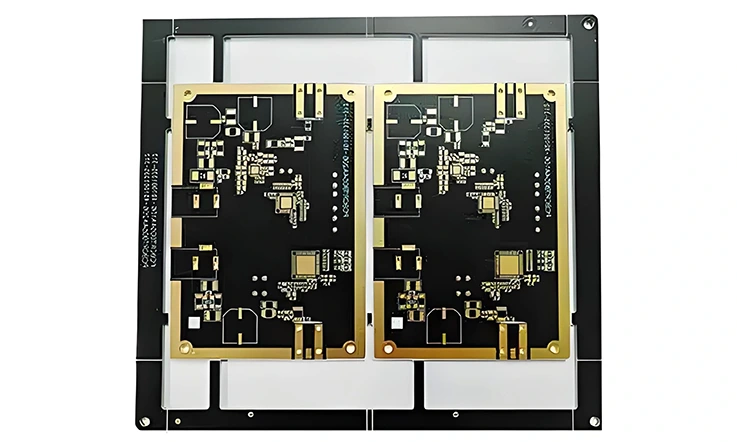
Advanced Structure Integration: From HDI to Rigid-Flex
The properties of IT-150GS are well-suited to address the specific production challenges of advanced interconnect technologies. Expert execution unlocks the ability to produce complex HDI, rigid-flex, and high-density BGA board architectures with high yield.
Blind, Buried, and Microvia Processing Capabilities
For HDI boards requiring sequential lamination, the material must withstand multiple bonding and thermal cycles while maintaining structural integrity and registration. The production process control makes this possible.
●Clean Microvia Formation: The laser drilling of microvias (0.1mm to 0.15mm) is controlled to produce clean hole walls with minimal charring, which enables complete and reliable electroless copper coverage for a solid plating base.
●Void-Free Via Filling: The via-in-pad process is managed under vacuum lamination to achieve a complete, void-free resin fill. This creates a solid, planar surface for mounting fine-pitch components directly on the via, a benefit for dense designs.
●High-Precision Registration: During the fabrication of stacked vias, layer-to-layer registration is maintained within ±25 µm, accommodating aggressive client designs with 50 µm trace and space features.
●Multi-Lamination Adhesion: A robust lamination process ensures that the resin-to-glass interface shows strong adhesion even after the repeated post-bake cycles required in complex, four-sequence HDI builds, preventing latent delamination issues in the final product.
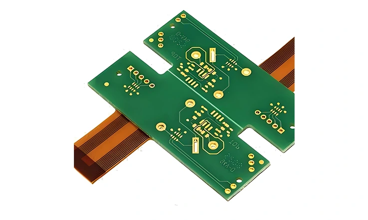
Techniques for Hybrid Lamination in Rigid-Flex Designs
One of the difficulties in rigid-flex boards lies in controlling the mechanical stress where the rigid and flexible sections meet. The well-matched Z-axis coefficient of thermal expansion between IT-150GS and polyimide-based flex materials presents an opportunity for precise process control to address this challenge effectively.
A recent client in the wearable technology space required a rigid-flex board that would endure thousands of flex cycles. The design was dense, but the real challenge was ensuring the integrity of the rigid-to-flex transition zone. The comparable Z-axis CTE of IT-150GS and the polyimide was the theoretical starting point. The manufacturing solution involved a proprietary plasma-etch process to enhance surface topography for adhesion, combined with a lamination cycle that used a staged pressure profile to minimize stress at the bond line. The final assemblies passed 100,000 flex cycles, far exceeding the client’s requirements.
●Boundary Zone Stress Reduction: A controlled lamination profile limits the mechanical stress concentrated at the rigid-flex transition zone during press cycles and solder reflow, a common point of failure.
●Precise Interface Processing: Clean laser ablation and precise coverlay placement are achieved without significant resin smear or fraying at the boundary, a testament to process control.
●Hybrid Adhesive Compatibility: The process ensures strong bonding performance with the specialized no-flow prepregs and epoxy-based adhesives commonly used in hybrid rigid-flex stackups.
Table: Rigid-Flex Integration Performance Metrics:
| Parameter | Value | Description |
| Z-Axis CTE (IT-150GS) | ~65 ppm/°C | Compatible with polyimide-based flex materials |
| Flex Cycle Test Result | >100,000 cycles | Exceeded client requirement in wearable application |
| Surface Treatment Method | Plasma-etch | Enhances adhesion for hybrid lamination |
| Bond Line Stress Management | Staged pressure profile | Reduces rigid-to-flex interface stress |
| Resin Smear at Boundary | Minimal | Achieved via precise laser ablation and clean coverlay cut |
BGA Pitch Optimization and Local Thermal Management
The production process must accommodate the fine features and tight tolerances required for high-I/O-count packages, including BGA designs with pitches below 0.4 mm.
●Surface Planarity for BGAs: The via fill and planarization processes are meticulously controlled. The outcome is a surface coplanarity that is held within ±15µm. This level of precision, verified by in-house 3D laser profilometry, is what allows clients to confidently assemble 0.4mm pitch BGAs with maximum yield.
●Advanced Via-in-Pad Support: The fabrication process is fully compatible with non-conductive via fill techniques (resin plugging and capping) to ensure excellent solder joint coplanarity on fine-pitch pads, preventing solder shorts or opens.
●High-Temperature Reflow Tolerance: The finished boards can withstand the demanding reflow profiles required for soldering high-density interposers and system-on-module components, which can have high thermal mass.
●Signal Integrity Beneath BGAs: The stable dielectric properties of IT-150GS allow for the reliable creation of controlled-impedance differential pairs in the dense breakout regions directly underneath BGAs.
Table: BGA and Thermal Handling Capabilities:
| Specification | Value / Capability |
| Surface Coplanarity (Post-Planarization) | ±15 µm |
| BGA Pitch Support | Down to 0.4 mm |
| Via-in-Pad Filling Technique | Non-conductive (resin plug + cap) |
| Reflow Temperature Tolerance | >260°C |
| Signal Integrity Support | Controlled impedance beneath BGA |
Proven Applications Across Demanding Industries
The combination of IT-150GS’s robust performance and a fabricator’s expert handling makes it a proven choice for multilayer PCBs across a range of demanding industries. Its adoption in these sectors is driven by a need for long-term reliability where electrical, thermal, and mechanical stability are non-negotiable.
Medical Devices and Portable Diagnostic Equipment
In medical electronics, where precision and patient safety are inextricably linked, the stability afforded by expert fabrication on IT-150GS is paramount.
●Case Study: Autoclave-Resistant Diagnostic Tool: A client developing a handheld diagnostic tool faced a formidable challenge: the device had to withstand repeated steam sterilization cycles without failure. The low moisture absorption of IT-150GS was the foundation. The manufacturing craft, however, lay in developing a proprietary sequential lamination and via-capping process. This resulted in a completely sealed, non-porous board. The final products passed the client’s rigorous 100-cycle autoclave test without a single failure, a testament to a process where material science meets manufacturing art.
●Fine-Pitch Assembly: The application of ENIG and Immersion Silver surface finishes on IT-150GS enables the reliable soldering of fine-pitch, medical-grade components.
●Miniaturization Support: The ability to fabricate dense via arrays with minimal drill smear supports the complex routing required to fit advanced functionality into small, ergonomic enclosures for medical clients.
Automotive ECUs and Industrial Control Systems
For automotive and industrial applications subject to constant thermal cycling, vibration, and mechanical stress, a board fabricated on IT-150GS offers a validated solution for robust, long-life electronics.
●Proven Via Reliability: The finished through-holes sustain integrity after rigorous thermal shock and solder float tests, evaluated according to demanding IPC-TM-650 methods.
●Assembly Process Compatibility: The fabricated boards work well with press-fit connectors and selective plating methods commonly used in the assembly of automotive ECU modules.
●Complex Stackup Support: The ability to perform sequential lamination supports the specialized power-and-ground-core builds found in powertrain and transmission control units.
●High-Temperature Soldering: The final product withstands the lead-free reflow profiles used in the assembly of components destined for engine bay and industrial control applications, where operating temperatures are elevated.
Consumer Electronics and High-Density IoT Devices
This material is widely used as the basis for high-volume consumer electronics, where a production facility must deliver performance in a compact and cost-effective form factor.
●High-Frequency Performance: The fabrication process maintains the dependable dielectric properties of the material at GHz frequencies, ensuring minimal signal attenuation for Wi-Fi, Bluetooth, and other wireless interfaces integrated into the device.
●Fine-Feature Fabrication: The clean drilling and complete via fill achieved during manufacturing aid in the compact integration of microcontroller and antenna modules for the client’s design.
●BGA and CSP Reliability: The ability to produce reliable plating thickness in small-diameter vias improves the solder joint reliability for fine-pitch BGA and CSP packages during assembly.
●Proven Field Durability: The finished boards exhibit robust dimensional stability across the wide temperature fluctuations experienced by outdoor or semi-industrial IoT devices over their operational lifetime.
TEQ IT-150GS vs. Isola 370HR from a Fabricator’s View
Choosing the right laminate extends beyond a datasheet comparison. This analysis is based on direct, hands-on experience fabricating multilayer boards with both ITEQ IT-150GS and Isola 370HR. The evaluation is from a practical manufacturing perspective, focusing on performance, processability, and total cost of ownership for the client.
Comparing Core Performance and Reliability Metrics
Table: Thermal Performance Comparison:
| Attribute | ITEQ IT-150GS | Isola 370HR |
| Tg (Glass Transition) | ~155°C | >180°C |
| T288 Delamination Time | >60 min @ 288°C | >60 min @ 288°C |
| Lead-Free Reflow Support | Yes (up to 260°C) | Yes (extended cycles) |
Thermal Performance:
●ITEQ IT-150GS: With a Tg of ~155°C, it reliably handles standard lead-free reflow profiles. Its T288 delamination time of over 60 minutes provides confidence for processing boards up to 12 layers in most commercial applications.
●Isola 370HR: Offers a higher Tg of >180°C. This provides a wider safety margin for assemblies with more than two reflow cycles or aggressive sequential lamination, common in the highest reliability sectors.
●Perspective: For a broad range of commercial and industrial products, a board built on IT-150GS provides more than sufficient thermal performance. 370HR is selected for designs where extreme thermal survivability is the primary design driver, such as in aerospace applications.
Electrical Performance:
●ITEQ IT-150GS: Its Dk of ~4.2 and Df of ~0.010 (@1GHz) allow for the production of circuits with good signal integrity for applications up to ~10 Gbps.
●Isola 370HR: Its slightly different Df (~0.016 @1GHz) is leveraged for applications where that specific loss profile is required, often for very long trace lengths in backplanes or 25 Gbps+ SerDes channels
●Perspective: IT-150GS is a highly cost-effective substrate for a wide range of high-speed digital designs. 370HR is specified when its particular electrical behavior and thermal properties are demanded by the application’s specific design constraints.
Table: Electrical Performance Comparison:
| Attribute | ITEQ IT-150GS | Isola 370HR |
| Dielectric Constant (Dk) @ 1GHz | ~4.2 | ~4.17 |
| Dissipation Factor (Df) @ 1GHz | ~0.010 | ~0.016 |
| Suitable Signal Speed | Up to ~10 Gbps | 25 Gbps+ |
Moisture Absorption:
●ITEQ IT-150GS: Exhibits low moisture uptake (~0.12%), which, in a controlled fabrication environment, ensures stability during assembly and reduces delamination risk.
●Isola 370HR: At ~0.15%, its absorption rate is also excellent.
●Perspective: Both materials, when handled properly during production, yield boards with excellent resistance to moisture-related failures. The choice between them on this metric is seldom a deciding factor.
Table: Moisture Absorption Comparison:
| Attribute | ITEQ IT-150GS | Isola 370HR |
| Moisture Absorption | ~0.12% | ~0.15% |
| Assembly Stability | High | High |
Evaluating Manufacturability and the Processing Window
Drillability:
●ITEQ IT-150GS:This material drills cleanly with minimal resin smear, allowing for long drill tool life and high-quality hole walls. High throughput and steadfast quality can be maintained.
●Isola 370HR:Its denser weave can lead to faster drill wear, sometimes requiring adjusted feed/speed rates or more frequent tool changes in high-volume production to maintain hole quality.
●Perspective:IT-150GS generally offers a more forgiving drilling process from a production standpoint, which can translate to lower tooling costs and more dependable results for the client.
Lamination and Resin Flow:
●ITEQ IT-150GS: Provides highly foreseeable resin flow in standard press cycles, allowing for excellent void-free bonding in typical multilayer stackups.
●Isola 370HR: Features a slightly wider processing window for lamination, which can be beneficial for very complex sequential lamination cycles in advanced HDI boards.
●Perspective: IT-150GS is exceptionally reliable for standard multilayer lamination. 370HR offers a degree of additional latitude for the most intricate HDI structures, which can be a benefit in production but often comes at a higher material cost for the client.
A Frank Look at Cost-Effectiveness and Supply Chain Realities
Material Price and Availability:
●ITEQ IT-150GS: Generally more economical and readily stocked across Asia with short lead times. We can pass these cost and time savings on to the client, making it a pragmatic choice for cost-sensitive projects.
●Isola 370HR: Priced at a premium, with strong availability in North America and Europe. It is often specified by end-customers in the telecom and enterprise sectors.
●Perspective: Boards built on IT-150GS offer a better total cost and supply chain advantage for many commercial projects. 370HR is the go-to for designs where its specific performance justifies the premium and its regional availability is advantageous.
Process Integration Cost:
●ITEQ IT-150GS: As a widely used Tg 150°C class material, it can often be processed with no changes to existing, qualified FR-4 workflows, reducing onboarding time and risk for a new project.
●Isola 370HR: Migrating a client’s design to 370HR may require a process re-qualification, especially for drilling and lamination parameters, adding to the initial setup effort and cost.
●Perspective: IT-150GS presents a lower barrier to entry and faster integration for most production facilities, translating to faster time-to-market for the client.
Meeting the Challenges of AI, EV, and 5G Hardware
Successfully fabricating hardware for AI, electric mobility, and 5G infrastructure requires more than just advanced processing; it demands the transformation of a material foundation into a product engineered for extreme thermal, electrical, and mechanical demands.
Board-Level Reliability for AI Edge Computing Devices
For AI inference hardware, where continuous thermal loads and high-density interconnects are standard, the fabrication process must deliver exceptional board-level reliability.
●Thermal Management Under BGAs: The process leverages the material’s thermal stability to maintain structural integrity through multiple reflows, preventing delamination under dense, heat-concentrating 0.4 mm pitch BGA arrays.
●Power Integrity for AI Loads: Compatibility with HDI processing allows for the creation of blind and buried via structures, enabling the low-impedance power planes needed to prevent voltage droop during intense AI acceleration cycles in the client’s device.
●Long-Term Solder Joint Durability: Controlling the Z-axis CTE during production minimizes stress on solder joints during thermal cycling, a known factor in improving the long-term reliability of high-I/O-count packages used in AI accelerators.
High-Current Performance for EV Inverters and Battery Management Systems
In automotive power electronics like inverters and Battery Management Systems (BMS), the manufacturing process must deliver boards with high-current capacity and long-term environmental endurance.
●Heavy Copper and High-Aspect-Ratio Vias:The production process is engineered to properly fill and bond with heavy copper layers (up to 3oz), while also supporting the high-aspect-ratio plated through-holes common in EV power boards.
●High-Voltage Clearance Control: Superior dimensional control during lamination is foundational for achieving the precise drill-to-copper clearances required in high-voltage designs, mitigating risks of field failure for the automotive client.
●Under-Hood Thermal Endurance: The finished boards offer stable performance at continuous operating temperatures, showing no resin cracking or copper delamination after extensive thermal shock testing, making them suitable for demanding IGBT modules and motor controls.
Signal Layer Stability for 5G Base Stations and Antennas
As 5G systems move to higher frequencies, the PCB must be fabricated as a predictable high-frequency component.
●Impedance Control for 5G Frequencies: The stable dielectric constant of IT-150GS is leveraged to achieve tight ±5% impedance control on 50Ω and 100Ω transmission lines in 8- to 16-layer baseband boards.
●Signal Loss Management: With a low dissipation factor, IT-150GS is a suitable material choice. Insertion loss on high-speed channels can be further managed by controlling copper roughness during the production process.
●Connector and Antenna Interface Stability: A process that yields low warpage and high planarity ensures the flat, reliable surfaces needed for the fine-pitch BGA, QFN, and LGA packages used in 5G antenna and beamforming arrays.
Beyond the Material – The Value of Expert Fabrication
The success of a high-performance printed circuit board is born from the union of a well-chosen material and a disciplined, insightful manufacturing process. ITEQ IT-150GS offers a remarkably balanced foundation of performance, reliability, and manufacturability.
A material itself is inert potential. Its true value is unlocked by the fabricator. It is realized in the precise control of a drill bit, the uniform pressure of a lamination press, and the deep understanding of how its chemistry reacts to the thermal journey of assembly.
This document has aimed to illuminate not just the properties of a laminate, but the philosophy behind transforming those properties into tangible, reliable performance in the final product. The selection of a production partner with this depth of understanding is what ultimately ensures a design’s intent is fully and faithfully realized.
FAQ:
1. What are the recommended storage and pre-baking conditions for IT-150GS before fabrication?
For optimal performance, IT-150GS should be stored in a dry environment (<50% RH). A pre-bake cycle (e.g., 2–4 hours at 120°C) is recommended before lamination, especially if the material has been exposed to high humidity.
2. What are the common glass fabric styles available for IT-150GS prepregs?
IT-150GS prepregs are available in various glass styles, including 106, 1080, 2116, and 7628. The choice affects dielectric thickness, impedance control, and resin content, and should be selected based on the specific stackup requirements.
3. Is IT-150GS recommended for analog RF applications, such as patch antennas?
While excellent for high-speed digital applications up to ~6-10 GHz, its dissipation factor (Df) is generally considered too high for sensitive, low-loss analog RF applications like filters or high-efficiency antennas, where specialized RF materials are better suited.
4. What are the standard supplied panel sizes for IT-150GS?
IT-150GS is commonly available in standard panel sizes such as 36″x48″, 40″x48″, and 42″x48″, allowing for efficient panelization and fabrication of various board dime


