Various materials and components play crucial roles in ensuring the efficient functioning of a circuit board. The printed circuit board (PCB) serves as the central component in the majority of electronic devices. However, specific materials are employed in the design of these circuit boards, with the PCB plate being a notable example.
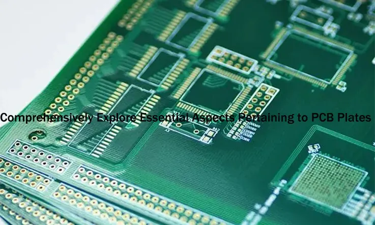
The PCB plate holds significant importance within a circuit board’s construction. PCBs fulfill the dual purpose of providing mechanical stability and electrical connectivity to electronic devices. Particularly in the realm of keyboard PCBs, the inclusion of a plate is common practice. In the following discourse, we will comprehensively explore essential aspects pertaining to PCB plates, providing you with a comprehensive understanding of their significance.
What is a PCB Plate?
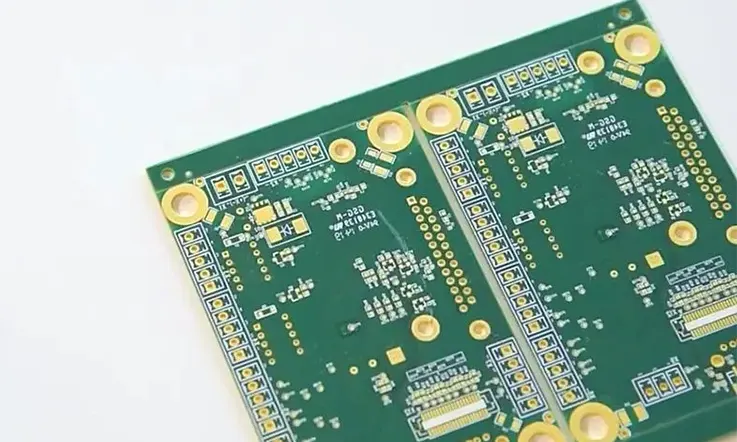
A PCB plate, also known as a PCB substrate or PCB base material, refers to a rigid or flexible board that serves as the foundation for mounting electronic components and creating electrical connections in a printed circuit board (PCB). It is essentially a flat, non-conductive material upon which the conductive traces, vias, and pads are etched or deposited.
The PCB plate is typically made of a layered composite material, which consists of an insulating substrate layer and a conductive copper layer. The insulating substrate is usually composed of materials like fiberglass-reinforced epoxy resin (FR-4), phenolic resin, polyimide, or ceramic. These materials offer excellent electrical insulation properties and mechanical strength to support the components and withstand various environmental conditions.
The conductive copper layer is patterned to form the desired circuitry on the PCB plate. It provides the pathways for electrical signals to flow between different components and facilitates the interconnection between them. The copper layer is etched or laminated onto the substrate using techniques such as chemical etching or additive plating, creating the desired circuit pattern.
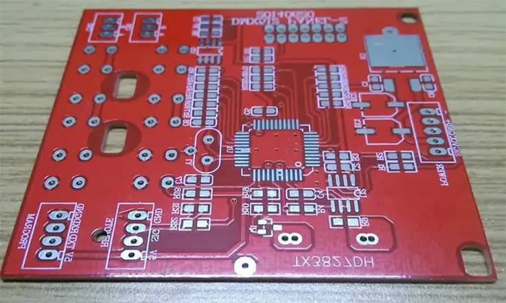
In addition to the substrate and copper layers, the PCB plate may also include other layers such as solder mask, silkscreen, and surface finish. The solder mask is a protective layer applied over the copper traces to prevent solder bridges and ensure proper soldering during assembly. The silkscreen layer contains component labels, markings, and other printed information for easier identification. The surface finish provides a protective coating and facilitates solderability.
Overall, the PCB plate is a fundamental component of a circuit board, providing the necessary mechanical support, electrical connectivity, and insulation required for the proper functioning of electronic devices. Its design and material selection play a crucial role in determining the performance, reliability, and manufacturability of the PCB.
Types of PCB Plate Materials
Here are some of the most common materials used for PCB plates:
FR-4 Glass Epoxy: The most popular PCB material. Good physical strength and electrical properties. Low cost.
CEM-1/CEM-3: Woven fiberglass reinforced epoxy laminates. Low loss, good high frequency performance.
FR-5: High Tg glass epoxy material. Withstands high temperatures. Good dimensional stability.
GETEK: Glass cloth reinforced epoxy. Low dielectric loss. Used for RF/microwave boards.
Polyimide: Flexible material used for flex PCBs. Withstands bending without damage. Examples: Kapton, Upilex.
Aluminum: Thermally conductive metal core PCBs use a base aluminum layer. Good for LED boards.
Ceramic PCBs: Alumina or aluminum nitride substrates have excellent thermal conductivity. Costly.
Rogers Laminates: Variety of premium and high frequency PCB materials with controlled dielectric properties.
Arlon Materials: Includes options like Thermoset polyester, PTFE composites, and ceramic filled PTFE.
Isola Laminates: Materials engineered for low loss, low Dk, high thermal performance, etc.
The choice depends on electrical, thermal, mechanical, and cost requirements. Material properties directly impact PCB performance and manufacturing processes.
PCB Plate Construction
Here are a few key things to know about PCB plate construction:
●PCB plates provide mechanical support and structure for the components mounted on the board. They are made from rigid insulating materials like FR4 fiberglass.
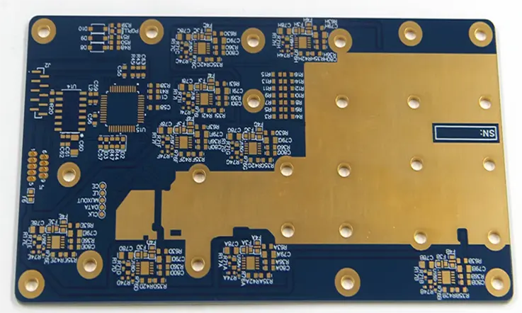
●PCB plates can be single-sided, double-sided, or multilayer. Single-sided have copper traces on one side, double-sided have copper on both sides, and multilayer have multiple copper layers separated by insulating dielectric.
●Traces and pads are formed by etching away unwanted copper, leaving the desired circuit pattern. This is done using photolithographic techniques to transfer the circuit design to the copper clad board.
●Holes are drilled in the board to mount components. Plated through-holes connect traces between layers. Vias connect traces between sides. Non-plated holes are used for mounting only.
●Solder mask is applied over the traces as an insulator and for corrosion resistance. Silkscreen printing applies markings for components.
●Boards can be fabricated as individual units or as arrays of multiple boards for mass production. They are cut or routed apart after fabrication.
●Edges of boards are often beveled to remove sharp corners. Stronger boards may have thicker copper layers and more fiberglass layers. Flexible boards use polyimide instead of FR4.
●Important fabrication specifications include trace width/spacing, number of layers, thickness, dielectric constants, etc. Proper design ensures manufacturability and reliability.
Functions and Types of PCB Plates
Printed Circuit Boards (PCBs) are central to modern electronics. Every electronic device contains a PCB of some sort, whether it’s a smartphone, a computer, or even a simple digital clock.
Functions of PCB Plates
Mechanical Support: PCBs provide a physical base on which to mount the electronic components. This ensures the components stay in place and remain interconnected even under physical stress.
Electrical Connectivity: The copper tracks on a PCB form the circuit. These tracks connect different electronic components in a specific sequence, enabling the flow of electricity.
Heat Dissipation: PCBs often have a layer dedicated to heat dissipation. This layer can help prevent overheating in high-power electronic components.
Design Simplification: PCBs simplify the process of assembling electronics. They make mass production possible by facilitating the duplication of a single, complex design.
Types of PCB Plates
Single-sided PCBs
Single-sided PCBs have only one layer of substrate or base material. The single layer consists of a thin layer of metal, typically copper (due to its excellent electrical conductivity), which is coated with a layer of protective solder mask and then printed with the circuit diagram.
Double-sided PCBs
Double-sided PCBs have a base material with a thin layer of conductive metal, like copper, applied to both sides of the board. Holes drilled through the board allow circuits on one side to connect to circuits on the other.
Multilayer PCBs
Multilayer PCBs have more than two layers (typically 4, 6, 8, or even more). The circuit layers are connected using plated through holes called vias. Multilayer PCBs allow for higher component density and design complexity.
Rigid PCBs
Rigid PCBs are those that are not designed to flex during use. These are the most common type, found in standard desktop computers, televisions, and other consumer electronics.
Flexible PCBs
Flexible PCBs are designed to bend and flex during use. They’re typically found in more complex and space-constrained electronics like satellites, medical equipment, and advanced telecommunications devices.
Rigid-Flex PCBs
Rigid-flex PCBs combine the best of both rigid and flexible circuit boards. They are produced in segments of rigid and flexible substrates and can be used in electronics where space is a premium.
High-frequency PCBs
These are a type of PCB designed to transmit signals over a high frequency. They are made from a special material that avoids the issues of signal loss and coupling that can occur at high frequencies.
Each type of PCB plate has its strengths and applications, and the choice of which to use depends on the specific requirements of the electronic device in question.
Design Considerations for PCB Plates
Here are some key design considerations when laying out and constructing PCB plates:
●Component placement – Position components to minimize trace lengths and facilitate routing between components. Keep high-speed signals away from noise sources.
●Trace width – Match trace widths to expected current loads. Wider traces for power distribution, narrower for signals. Follow industry guidelines for trace width/clearance.
●Routing – Use 45 and 90 degree angles in traces as much as possible. Avoid acute angles. Use tidy orthogonal routing patterns.
●High speed signals – Maintain controlled impedances for traces, use ground planes, and provide shielding for EMI reduction.
●Power and ground – Use entire planes for power and ground distributions. Provide multiple vias for connections. Decouple power supplies with bypass capacitors.
●Layer stacking – Mindful layering with power/ground planes between signal layers. Route critical signals on inner layers.
●Board thickness – Thicker boards are more rigid and resist warping. More layers allow complex routing.
●Materials – FR4 glass epoxy is common. High frequency boards use materials with controlled dielectric constants.
●Copper weight – Heavier copper layers handle higher current loads. Thicker copper is more costly.
●Component footprints – Follow manufacturer recommendations for pad shapes and sizes. Account for heat dissipation needs.
●Silkscreen – Provide clear markings for polarities, pin 1 indicators, values, and other annotations.
●Finishes – Pick soldermask/silkscreen colors and ENIG/Immersion Gold/HASL surface finishes appropriately.
●Testing – Simulate designs thoroughly. Prototype and perform signal integrity testing before full production.
PCB Plates Manufacturing Process
Design and Layout – The circuit is designed and the PCB layout is created using EDA software like Altium, Eagle, OrCAD, etc.
Prototyping – Initial prototypes are often made to verify the design before full production. This uses similar fabrication steps but on a smaller scale.
Panelization – For mass production, the PCB layouts are arranged in a panel that optimizes board space and routing.
Lamination – Sheets of copper clad FR-4 or other dielectric material are stacked and laminated together using heat and pressure. This forms the multilayer board.
Drilling – Small holes are drilled through the board to form vias and mounting holes using CNC drilling machines.
Plating – The walls of the drilled holes are plated with copper electrochemically to form conductive paths between layers.
Etching – Unwanted copper is etched away chemically leaving only the desired copper traces.
Solder mask – A layer of epoxy ink is applied to protect traces and expose solder pads.
Silkscreen – Printing applied for markings like text, symbols, component outlines.
Routing/Scoring – Individual PCBs are routed or scored from the larger panels.
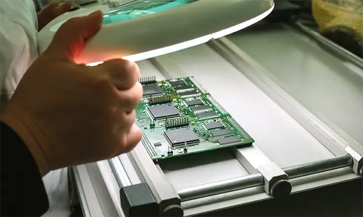
Electrical Testing – Each board is electrically tested to verify connectivity and function.
Population – Electronic components are soldered onto the board either by hand or using SMT pick-and-place machines.
Final Assembly – Connectors, brackets, and other hardware are assembled onto the populated board.
Final Testing – Comprehensive functional testing of the fully assembled board.
Application of PCB Plate
Here are some of the key applications and uses of printed circuit board (PCB) plates:
Keyboards: PCB plates provide mechanical support and stabilization for individual key switches in keyboard construction. They minimize key wobble during use.
Computers: Motherboards, backplanes, and interface cards utilize PCB plates for mounting components and interconnecting devices.
Consumer Electronics: Game consoles, TVs, home appliances rely on PCBs for circuitry and connectivity. The rigid plates provide structure.
Automotive: PCB plates integrate electronics for engine control units, infotainment, GPS, and other in-vehicle systems.
Telecom/Networking: Servers, routers, switches, and other network gear are built on multilayer PCB plates.
Industrial Equipment: PLCs, HMIs, and other controls use PCBs for automation and machine interfacing.
Medical Devices: Diagnostic systems, imaging tools, and patient monitors use rigid, durable PCB plates.
Military/Aerospace: Rugged PCBs withstand vibration and extremes in defense and avionics systems.
IoT Devices: Compact PCB plates interconnect sensors, processors, and wireless modules.
Audio Equipment: PCBs form the foundation for amplifiers, effects, mixing boards.
Summary
Engineered construction of PCB plates is fundamental to modern electronics, enabling complex, compact, and robust circuit assembly across countless applications.
Therefore, PCB plates enable connectivity, component mounting, and structure in virtually all modern electronics across consumer, industrial, and specialized applications.