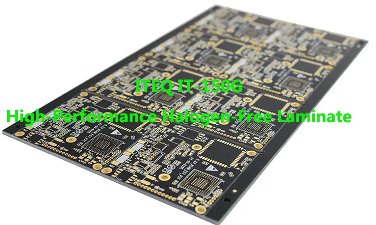
In the intricate dance of modern electronics, the printed circuit board serves as the stage. For demanding applications where performance and endurance are non-negotiable, the choice of substrate material is the first, most defining step. ITEQ IT-150G, a halogen-free, mid-Tg laminate system, emerges not merely as a component, but as a conscious choice for reliability. This guide moves beyond the datasheet, offering a deep exploration of IT-150G’s character, revealing how its inherent properties are unlocked through sophisticated fabrication and insightful design to create electronic assemblies of exceptional caliber.
ITEQ IT-150G: Core Technical Specifications
To truly understand a laminate, one must look beyond the numbers and appreciate its personality under stress. These specifications are the language the material uses to describe its behavior, from the heat of the reflow oven to the rigors of long-term operation.
Thermomechanical Properties
Here, we examine the material’s physical fortitude—its ability to hold its form and integrity when subjected to the thermal violence of assembly and the subtle strains of a thousand operational cycles.
| Property | Value | Notes |
| Glass Transition Temperature (Tg) | ~150°C | Maintains rigidity under soldering heat |
| Decomposition Temperature (Td) | ≥ 325°C | High thermal endurance |
| Time to Delamination (T260) | ≥ 60 min @ 260°C | Strong layer bonding |
| Time to Delamination (T288) | ≥ 10 min @ 288°C | Withstands lead-free reflow |
| Z-Axis CTE (50°C–260°C) | ~3.0% | Controls expansion stress |
| Peel Strength (1 oz copper) | ≥ 1.05 N/mm | Reliable copper adhesion |
●Glass Transition Temperature (Tg): At approximately 150°C, the Tg represents a threshold of composure. Below this temperature, IT-150G maintains a rigid, glassy certainty. Its mid-range value provides a stable foundation that resists twisting or bowing during the intense heat of lead-free soldering, ensuring the geometric precision of the final assembly.
●Decomposition Temperature (Td): Rated at a formidable 325°C or higher, the Td is the material’s ultimate thermal breaking point. This high ceiling offers a generous safety margin, a thermal buffer that protects the resin system from degradation during the multiple lamination and reflow cycles that complex boards must endure.
●Time to Delamination (T260 / T288): These values—≥ 60 minutes at 260°C and ≥ 10 minutes at 288°C—are a measure of the material’s endurance. They quantify how long the layers will remain bonded under extreme thermal stress, a direct testament to its resilience against the delamination failures that can plague lesser materials in a lead-free world.
●Z-Axis Coefficient of Thermal Expansion (CTE-Z): With a total expansion of approximately 3.0% from 50°C to 260°C, IT-150G exhibits a restrained response to heat in the vertical axis. This controlled expansion is a kindness to the plated-through holes, minimizing the stress on the copper barrels during thermal cycling and safeguarding the delicate vertical interconnects from cracking.
●Peel Strength: At ≥ 1.05 N/mm for 1oz copper, this figure speaks to the tenacity of the bond between the copper circuitry and the dielectric heartwood. This intimate connection ensures that pads and traces remain firmly anchored, resisting the forces of thermal shock and mechanical stress.
Electrical Performance Characteristics
These properties define the laminate’s role as a silent, steadfast conduit for electrical signals. They dictate the clarity of communication and the integrity of power within the system.
| Property | Value | Notes |
| Dielectric Constant (Dk) | ~4.4 @ 1 GHz | Stable impedance control |
| Dissipation Factor (Df) | ~0.017 @ 1 GHz | Low signal loss |
| Volume Resistivity | > 10¹⁰ Ω·cm | Strong insulation |
| Surface Resistivity | > 10¹⁰ Ω | Prevents leakage |
| Dielectric Breakdown Voltage | > 50 kV | Withstands high voltage |
●Dielectric Constant (Dk): A stable Dk of approximately 4.4 at 1 GHz makes IT-150G a predictable medium for electromagnetic waves. This predictability is the foundation of accurate impedance modeling, allowing for the design of transmission lines that carry high-speed data with minimal reflection or distortion.
●Dissipation Factor (Df): With a value of approximately 0.017 at 1 GHz, the dissipation factor measures the small fraction of signal energy that is absorbed and lost as heat. IT-150G’s moderate loss tangent makes it a fitting choice for systems where signal attenuation must be carefully managed, preserving the vitality of the signal as it travels across the board.
●Volume & Surface Resistivity: Exceeding 1010Ω, these high resistivity values affirm the material’s profound insulating capabilities. This ensures that electrical currents remain confined to their intended paths, preventing leakage even under challenging temperature and humidity conditions, thus upholding the long-term reliability of the assembly.
●Dielectric Breakdown Voltage: Rated above 50 kV, this indicates the material’s ability to withstand immense electrical pressure before yielding. It provides a substantial margin of safety for high-voltage and power applications, preventing catastrophic electrical failure.
Environmental & Safety Compliance
A modern electronic material must be a responsible citizen of a global marketplace, meeting stringent standards for environmental stewardship and operational safety.
| Property | Value | Notes |
| Moisture Absorption | < 0.15% | Minimizes water-induced defects |
| Flammability Rating (UL) | 94V-0 | Self-extinguishing, flame-retardant |
| Halogen-Free Compliance | RoHS / IEC 61249-2-21 | Meets environmental safety standards |
●Moisture Absorption: With a low affinity for moisture (less than 0.15%), IT-150G resists the ingress of water, a common catalyst for failure during assembly. This hydrophobic nature helps prevent delamination and other moisture-related defects, while also streamlining manufacturing by reducing the need for lengthy, time-consuming pre-baking cycles.
●Flammability Rating: A UL 94V-0 classification is the highest standard for flammability in plastics. It is an assurance that the material will quickly self-extinguish if exposed to flame, a fundamental safety requirement for nearly all electronic devices.
●Halogen-Free Composition: Full compliance with RoHS and IEC 61249-2-21 standards confirms IT-150G’s commitment to environmental health. By eliminating bromine and chlorine compounds, it meets the demands of the world’s most environmentally conscious markets.
Advanced Fabrication Processes for IT-150G PCBs
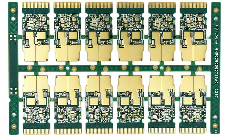
The journey from a simple sheet of laminate to a complex, multi-layered neurological system is one of precision and control. It is in the fabrication process that the true potential of IT-150G is awakened, where its properties are honed and shaped to create a foundation of unparalleled reliability.
Drilling Operations: The Genesis of Interconnection
The creation of a via is an act of controlled violence, a hole bored through the heart of the dielectric. The quality of this initial step echoes through the entire life of the board.
●Mechanical Drilling: The filled resin system of IT-150G responds to the drill bit with a clean cut, producing smooth, well-defined hole walls even in high-aspect-ratio designs. Automated drill management systems, tracking tool wear down to the micron, ensure that every hole is formed with a pristine edge, free from the tearing and smearing that can compromise plating adhesion.
●Laser Ablation for Microvias: In the microscopic realm of HDI, focused beams of light—both CO₂ and UV—carve out microvias with surgical precision. The material’s composition allows it to sublimate cleanly under the laser’s energy, leaving a residue-free landing pad at the bottom of the via, ready for a perfect metallurgical bond.
●Hole Wall Preparation: After drilling, the hole wall is meticulously prepared through a plasma or permanganate desmear process. This step not only cleans the surface but also texturizes it, creating a microscopic landscape that invites a tenacious, unbreakable bond with the first layer of electroless copper, the seed from which the entire conductive via will grow.
Lamination: Forging Unity from Layers
Within the lamination press, under immense heat and pressure, individual layers are fused into a single, monolithic entity. It is a process of transformation, where the prepreg’s resin flows like molten glass to create a solid, void-free structure.
●Predictable Resin Flow: The IT-150G prepreg is engineered for a well-mannered, predictable resin flow. It moves with purpose, completely encapsulating the intricate copper patterns of the inner layers without creating resin-starved deserts or undesirable voids that could compromise the board’s dielectric integrity.
●Dimensional Composure: Throughout the intense lamination cycle, IT-150G maintains its dimensional composure, exhibiting minimal shrinkage or warpage. This stability is the key to achieving the precise layer-to-layer registration demanded by today’s dense, complex designs, ensuring that every via finds its target.
●Sequential Lamination Endurance: For advanced HDI boards requiring multiple trips to the press, IT-150G demonstrates remarkable endurance. It withstands repeated thermal cycles without losing its structural integrity, allowing for the construction of stacked microvia architectures and other complex 3D interconnects.
Surface Finishing: The Final Interface
The surface finish is the board’s handshake with the outside world—the critical interface for soldering and connection. IT-150G’s receptive surface chemistry allows for a wide wardrobe of finishing options.
●Process Versatility: The substrate is a welcoming host to a full suite of industry-standard finishes, from the golden luster of ENIG and ENEPIG to the organic simplicity of OSP and the silvery sheen of Immersion Silver. The chemical baths for these processes are maintained in a state of perfect equilibrium through continuous statistical process control.
●Noble Metal Performance: On the surface of IT-150G, ENIG and ENEPIG finishes form a dense, low-porosity layer that is exceptionally flat and durable. This pristine surface is ideal for the challenges of fine-pitch BGA mounting and delicate wire-bonding operations. X-ray fluorescence (XRF) systems verify the precise thickness of these precious metal layers on every panel.
●OSP Integrity: An OSP coating applied to IT-150G provides a robust, solderable surface that maintains its performance through an extended shelf life, offering an effective and environmentally sound alternative to metallic finishes.
Comparative Analysis: Strategic Positioning of IT-150G Laminates
Selecting a laminate is an exercise in understanding trade-offs and finding the optimal balance for a specific application. IT-150G does not exist in a vacuum; its value becomes clear when viewed in context with its peers, revealing its strategic position in the vast ecosystem of circuit board materials.
A Decisive Advantage Over Standard FR-4
IT-150G presents a clear and compelling upgrade in thermomechanical robustness for designs that demand more than what standard FR-4 can offer.
| Feature | Standard FR-4 | IT-150G | Improvement |
| Delamination Time (T288) | ~1–3 min | ≥ 10 min | ~10× better |
| Z-Axis CTE (50–260°C) | ~4.0–5.0% | ~3.0% | Reduced PTH stress |
| Manufacturing Process Window | Narrow | Wider, more stable | Fewer defects, better yield |
| Assembly Cycle Tolerance | Moderate | High | Better for lead-free & multilayer builds |
●Superior Thermal Endurance: It exhibits a tenfold or greater increase in delamination resistance (T288) compared to FR-4, providing a far more resilient foundation for surviving multiple, high-temperature lead-free assembly cycles.
●Enhanced PTH Reliability: A significantly lower Z-axis thermal expansion (CTE) minimizes the mechanical stress exerted on plated-through-hole barrels during temperature changes. This directly translates to a lower risk of via fatigue and cracking, a fundamental improvement for long-term reliability.
●Wider, More Forgiving Process Window: The material’s inherent stability provides greater manufacturing latitude, reducing the risk of defects and increasing yield for complex, high-layer-count boards.
A Pragmatic Position Relative to High-Tg Materials
While elite high-Tg materials like IT-180A serve the most extreme thermal environments, IT-150G distinguishes itself as the pragmatic and intelligent choice for a vast range of demanding applications.
| Feature | IT-150G | IT-180A (High-Tg) | Assessment |
| Glass Transition (Tg) | ~150°C | ~180°C | Suitable for most high-reliability needs |
| Decomposition Temperature | ≥ 325°C | ≥ 340°C | Excellent thermal margin for most applications |
| Target Applications | Industrial, server, telco | Harsh thermal extremes | IT-150G fits 80–90% of demanding scenarios |
| Cost | Moderate | High | Better cost-performance balance |
●Targeted for Demanding Mainstream Applications: It is perfectly suited for the challenging operational environments found in servers, telecommunications hardware, and industrial controls, where absolute reliability is required but the extreme conditions demanding a full high-Tg system are not present.
●Substantial Thermal Headroom: Its Tg of ~150°C and Td of ≥ 325°C provide more than enough thermal stability to ensure integrity and performance for the vast majority of high-reliability products.
●Optimized Cost-to-Performance Ratio: IT-150G masterfully occupies the strategic space where elevated performance intersects with intelligent economics, delivering a significant reliability upgrade without the full cost implication of higher-specification materials.
The Strategic Balance of Performance and Value
Ultimately, IT-150G’s identity is defined by its exceptional balance, serving as a powerful bridge between standard materials and costly specialty laminates.
| Parameter | Standard FR-4 | IT-150G | Benefit |
| Dielectric Constant (Dk @1GHz) | ~4.6–4.8 | ~4.4 | Better impedance control |
| Dissipation Factor (Df @1GHz) | ~0.020–0.025 | ~0.017 | Improved signal integrity |
| Cost | Low | Moderate | High value without high premium |
| Application Fit | Basic consumer boards | High-reliability, mid-speed systems | Ideal performance step-up |
●Meaningful Electrical Improvement: It offers a more stable dielectric constant for tighter impedance control and a lower dissipation factor for better signal integrity than FR-4, preserving the clarity of mid-speed digital signals.
●The Ideal Performance Step-Up: It is the logical and cost-effective choice for designs that are beginning to push the performance limits of FR-4 but do not require or cannot justify the expense of specialized RF/microwave materials.
●An Investment in Total Reliability: Choosing IT-150G is an investment in the entire product lifecycle. Its properties contribute to higher manufacturing yields, greater product longevity in the field, and superior overall system integrity.
Front-End Engineering for IT-150G: DFM and Stack-up Validation
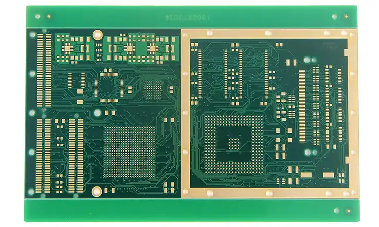
The journey from a digital design file to a tangible, high-performance circuit board is fraught with potential pitfalls. True manufacturing excellence begins long before the first piece of laminate is touched, in the cerebral realm of front-end engineering and Design for Manufacturability (DFM) analysis. This is not a mere checklist; it is a deep, collaborative dialogue with the design itself, ensuring that its intent can be translated into reality with precision and efficiency.
Validating the Architectural Intent
The stack-up is the soul of the board. Before committing it to the physical world, it must be rigorously interrogated to confirm its viability.
●Material and Stack-up Verification: The proposed combination of IT-150G cores and prepregs, including their specific glass weaves and resin content, is meticulously cross-referenced against the design’s electrical and physical demands. This ensures the chosen architecture can deliver the required impedance, dielectric separation, and overall thickness.
●Impedance Model Correlation: The design’s impedance targets are not taken at face value. They are independently modeled using sophisticated 2D field solvers, populated with the specific, measured characteristics of the IT-150G batch to be used. The simulation’s output is then reconciled with the design, flagging any discrepancies in trace geometry and ensuring the final product performs exactly as intended.
●Anticipating Resin Flow: For boards featuring dense component arrays or large copper planes, the lamination process is simulated. This virtual pressing anticipates how the IT-150G prepreg’s resin will flow, ensuring it will fully encapsulate every feature and prevent subtle voids that could compromise reliability down the line.
Foreseeing and Mitigating Fabrication Challenges
A seasoned eye can spot trouble in a design file miles away. DFM analysis applies this experience systematically, addressing the specific nuances of fabricating with IT-150G.
●Geometric Hazard Identification: Automated tools, guided by decades of fabrication knowledge, scan the design data for geometric traps. Acute angles that might capture etching fluids (“acid traps”) or perilously thin copper features (“slivers”) that could detach and cause shorts are identified and flagged for modification.
●Annular Ring Assurance: The analysis algorithmically verifies that the copper ring surrounding every drilled hole provides a sufficient connection point, meeting or exceeding the stringent requirements of IPC-6012 Class 3 for high-reliability products. This scrutiny extends to the microscopic target pads for laser-drilled microvias, ensuring their integrity.
●Optimizing for Assembly: The DFM process extends its view to the final assembly stage, verifying adequate clearances in the solder mask to prevent bridging and ensuring that silkscreen markings do not impinge upon solderable surfaces. This foresight prevents assembly-line headaches and contributes to a smoother, faster new product introduction.
Application Spotlight: Mastering a High-Vibration Industrial Controller
Theory is illuminating, but application is definitive. Let us consider a real-world challenge: the development of a compact, high-power motor control unit destined for a demanding industrial automation environment.
1.The Challenge: A Crucible of Heat and Vibration
The design specifications presented a formidable set of concurrent challenges. The controller had to operate flawlessly on a factory floor, mounted directly to machinery where it would be subjected to constant, high-frequency vibrations and ambient temperatures often exceeding 60°C. Furthermore, its compact enclosure required a dense component layout, including a powerful processor in a fine-pitch BGA package that generated significant localized heat. Failure was not an option, as any downtime on the factory line would result in substantial financial losses. The project demanded absolute long-term reliability in a punishing environment.
2.The Solution: A Synthesis of Material and Method
A multi-faceted approach was required, where the choice of material and the fabrication methodology were inextricably linked.
●Material Foundation: IT-150G was selected as the foundational material. Its Tg of 150°C provided ample margin above the operating temperatures, ensuring the board remained rigid and stable. Crucially, its robust mechanical properties and the strong adhesion between its resin and glass weave offered superior resistance to the micro-cracking and interconnect fatigue that can be induced by constant vibration. It offered a significant reliability upgrade over standard FR-4 without the cost burden of a full high-Tg system.
●Thermally-Aware Design: An 8-layer, symmetrical stack-up was designed to ensure board flatness and prevent warpage. A dense array of thermal vias was placed directly beneath the BGA processor, creating an efficient thermal conduit to pull heat away from the component and spread it across the large internal ground planes, which were specified with 2oz copper for enhanced heat spreading.
●High-Density Fabrication: To accommodate the tight layout, via-in-pad technology was employed for the BGA. The vias were meticulously filled and planarized to create a perfectly flat surface for soldering. The DFM review prior to fabrication was instrumental, identifying the need to slightly adjust copper pour clearances to ensure complete resin fill during lamination, preventing any potential voids that could compromise CAF resistance.
●Building for Endurance: All plated-through holes were fabricated using a pulse-plating process to guarantee a uniform and ductile copper barrel, adding a further layer of defense against thermal and mechanical fatigue. A resilient ENIG surface finish was chosen for its durability and excellent solderability, ensuring robust connections that would not degrade over time due to vibration.
3.The Outcome: Unwavering Reliability in the Field
The resulting IT-150G circuit board was more than just a component; it was a testament to a holistic design and manufacturing philosophy. The finished controllers passed rigorous HALT/HASS (Highly Accelerated Life Test/Stress Screen) testing with zero failures. Deployed in the field, they have demonstrated unwavering performance, proving that the intelligent pairing of a high-performance material like IT-150G with deep fabrication expertise is the true formula for creating products that endure.
Quality Assurance for High-Reliability IT-150G Fabrication
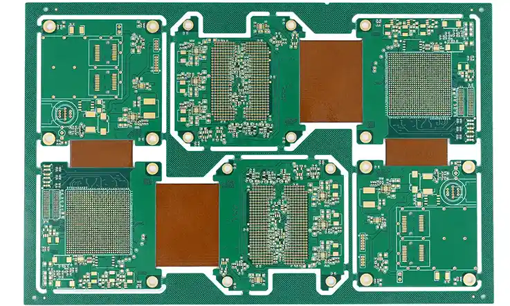
Every step in the manufacturing journey is an act of quality assurance. The final verification stages serve as the ultimate attestation that the finished IT-150G assembly is not only compliant with its design, but is a physical embodiment of reliability.
Witnessing the Inner Truth
A board’s quality cannot be judged by its surface alone. A series of tests provides a window into its internal structure and electrical soul.
1.Microsectional Analysis:
Test coupons, small avatars of the main board, are periodically sacrificed. They are cross-sectioned, their inner landscapes polished to a mirror finish and examined under high magnification. This reveals the intimate details of the board’s construction: the thickness and uniformity of the copper plating inside the vias, the quality of the metallurgical bond between layers, the very integrity of its vertical heart.
2.Unbroken Connectivity Test:
Every single finished board undergoes a comprehensive electrical test. Flying probe or bed-of-nails testers become a digital nervous system, methodically checking every pathway on the board to guarantee that the final connectivity map is a perfect one-to-one match with the original design file, with no opens or shorts.
3.Impedance Validation:
For boards where signal timing is measured in picoseconds, TDR testing provides the final word on impedance control. It sends a signal pulse down dedicated test traces on a coupon and analyzes the reflection, providing a precise, quantitative measurement of the characteristic impedance to confirm it is within its specified tolerance.
The Promise of Purity and Conformance
The final steps ensure the board is delivered in a state of pristine cleanliness and with full documentation of its pedigree.
1.Ionic Cleanliness Verification:
A board must be chemically, as well as electrically, pure. Ionic contamination testing is performed to ensure that no harmful residues from the fabrication process remain on the surface, as these could lead to electrochemical migration and latent field failures.
2.The Inspector’s Final Gaze:
A trained human inspector gives every board a final, meticulous visual examination. This is a search for subtlety—the quality of the solder mask, the legibility of the silkscreen, the uniformity of the surface finish—a final confirmation that the board is aesthetically, as well as functionally, perfect.
3.The Certificate of Conformance:
More than a piece of paper, the Certificate of Conformance (CoC) is a formal declaration. It is a traceable document that attests that the board has been forged in a controlled process, inspected to the highest standards, and has met every specification of the design and the relevant IPC industry standards. It is the final promise of quality, delivered.
The JarnisTech Advantage: A Synthesis of Technology, Quality, and Partnership
Understanding a material like IT-150G is only the first step. Transforming it into a flawless, reliable printed circuit board that performs perfectly in a mission-critical application requires a partner whose capabilities extend far beyond the basics of fabrication. It requires a synthesis of leading-edge technology, an unwavering commitment to quality, and a spirit of true partnership. This is the JarnisTech advantage.
Technological Mastery That Empowers Your Design
We view technology not as a feature, but as a tool to unlock your design’s full potential. Our continuous investment in state-of-the-art capabilities—from CO₂/UV laser drilling for microscopic HDI features, to pulse plating for high-aspect-ratio via reliability, and automated optical/X-ray inspection—means fewer design constraints for you. It translates into greater miniaturization, higher performance, and the confidence that even your most ambitious designs can be brought to life with precision.
A Culture of Uncompromising Quality
For us, quality compliant with standards like AS9102 and IPC Class 3 is not a department; it is the language our entire operation speaks. From rigorous raw material validation to final microsection analysis, we build quality into every step. This obsession with detail ensures that each board we deliver is not only dimensionally and electrically perfect, but also possesses the hidden, intrinsic reliability to withstand the test of time and the rigors of its end environment. We deliver peace of mind.
Value Optimization, Not Just Pricing
We believe in intelligent economics. Our focus is on optimizing the Total Cost of Ownership for your project. Through insightful DFM feedback that enhances yield, efficient material utilization, and a fabrication process that eliminates rework and scrap, we reduce unnecessary costs. By delivering a board that prevents costly field failures, we provide a superior long-term return on your investment.
Predictability and Transparency in Delivery
In today’s fast-moving market, meeting your timeline is paramount. Our strength lies in predictability. Through strategic inventory management of key materials like IT-150G and a transparent, data-driven production scheduling system, we provide realistic and reliable lead times. We communicate proactively, ensuring you have the visibility needed to manage your project and meet your market windows with confidence.
An Engineering Partnership, Not Just a Service
What truly sets us apart is our role as an extension of your team. Our front-end application engineers are your dedicated partners. They invest the time to understand the unique challenges and goals of your project, offering consultative support that goes far beyond a simple transaction. From stack-up design to assembly guidance, we are committed to one thing: your success.
Final Words
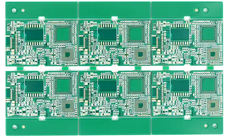
In the final analysis, ITEQ IT-150G reveals itself to be more than a set of impressive specifications. It is a canvas of immense potential. Its true value is unlocked not in isolation, but through its synthesis with a fabrication process that is both a science and an art. The material’s inherent robustness, when shaped by a deep understanding of its character and a manufacturing environment dedicated to precision and control, gives rise to printed circuit boards that are the bedrock of reliable, high-performance electronics. This fusion of superior material science with masterful fabrication creates a platform that is at once dependable and enabling, providing the foundation upon which enduring technology is built.
Begin Your High-Reliability Project Journey
Reading about capability is one thing; applying it to your unique challenge is another. We invite you to take the next step. Choose the path that best suits your current needs, and let us begin the dialogue that transforms complex designs into tangible, reliable hardware.
1.Request a Technical Consultation
Schedule a complimentary, no-obligation consultation with our application engineers. We can help you navigate complex material selection, stack-up design, and technology choices for your specific project.
2.Submit for a Manufacturability Review
Upload your design files through our secure portal for a comprehensive DFM (Design for Manufacturability) analysis. Our front-end engineering team will provide valuable feedback to identify opportunities for yield enhancement, cost optimization, and risk mitigation before fabrication begins.
3.Obtain a Project Quotation
For projects with defined specifications, receive a detailed and transparent quotation. Understand the full scope of our capabilities and how we can bring your IT-150G printed circuit board project to life with precision and efficiency.
FAQs about ITEQ IT-150G
1. What are the challenges of laminating IT-150G with high-frequency RF materials in hybrid builds?
It requires a carefully profiled press cycle to manage the different thermal expansion rates at the material interface and prevent internal stress.
2. What is the practical limit for heavy copper designs with IT-150G?
It handles 2 oz and 3 oz copper well. Heavier weights (≥4 oz) are achievable but require special attention to resin flow during lamination to ensure proper encapsulation.
3. Is the material’s surface suitable for Laser Direct Imaging (LDI) for sub-75μm features?
Yes, its smooth surface is well-suited for LDI, enabling the definition of very fine trace and space geometries with high accuracy.
4. What is a typical etch factor observed with IT-150G using standard chemistry?
Using standard ammoniacal etching, it exhibits good line definition with minimal undercut, supporting the fabrication of tightly controlled impedance traces.
5. Is it advisable to stack multiple plies of low-resin-content IT-150G prepreg to build thickness?
It is possible but not ideal. Using a single ply of a higher-resin-content prepreg is preferred to ensure complete resin flow and prevent potential voids or fill issues.
6. From a yield and cost perspective, what is the material’s process “sweet spot”?
It provides an excellent balance for 6 to 12-layer HDI boards that require lead-free assembly but do not need the extreme thermal capacity (and cost) of very high-Tg materials.

