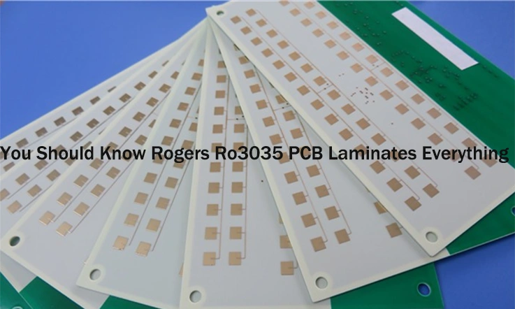
An Introduction to Rogers RO3035:
As communication and sensing technologies extend into microwave and millimeter-wave ranges, PCB laminates encounter greater demands. Higher data rates in 5G/6G, 77 GHz automotive radar, and satellite links require substrates that minimize signal loss, reduce phase distortion, and maintain thermal stability. Conventional materials like FR-4 struggle under these conditions, increasing the chance of system issues.
Choosing an appropriate PCB laminate matters. Rogers RO3035 delivers reliable electrical performance and mechanical strength suitable for these applications. This guide offers a thorough overview of RO3035, including its material traits, circuit design considerations, simulation techniques, and manufacturing methods aimed at producing dependable, high-performing circuit boards with good yield.
Defining RO3035: Composition and Core Attributes
The fundamental composition of RO3035 sets it apart from conventional epoxy-based laminates like FR-4. Its architecture is built upon a PTFE base infused with specialized ceramic fillers.
●PTFE Base: The PTFE matrix is responsible for the material’s inherently low dielectric constant and low dissipation factor. This polymer exhibits minimal electrical loss, allowing electromagnetic waves to propagate through it with very little energy dissipation as heat.
●Ceramic Fillers: The ceramic particles are precisely formulated to enhance the laminate’s characteristics. They contribute to the exceptional stability of the dielectric constant over temperature and frequency. Additionally, the ceramic content improves the material’s dimensional stability by lowering its coefficient of thermal expansion (CTE), bringing it closer to that of copper.
Key Differentiators in High-Frequency Applications
The combination of PTFE and ceramic fillers yields a unique profile that directly addresses the challenges of high-frequency circuit design.
●Electrical Predictability: The material exhibits uniform electrical properties, lot after lot. This predictability allows simulation models to align closely with the performance of physical circuit boards, reducing design iterations and accelerating time-to-market.
●Structural Integrity: The low Z-axis CTE ensures the reliability of plated through-holes (PTHs) during thermal cycling, a common failure point in less stable materials. This is especially beneficial in multilayer constructions and in environments with significant temperature swings.
●Low Moisture Absorption: RO3035 has a very low moisture absorption rate (typically 0.04% per ASTM D570). This characteristic prevents shifts in dielectric properties in humid environments, ensuring stable performance for outdoor or environmentally exposed applications.
Comparative Analysis: RO3035 vs. Other High-Frequency Materials
Selecting the appropriate laminate involves an evaluation of electrical performance, manufacturing complexity, and project cost. The Rogers portfolio includes several families of materials, each tailored for different segments of the RF market. A comparison between RO3035 and its counterparts—RO3003, RO4350B, and RO4003C—clarifies its specific application space.
Electrical Performance Benchmarking: RO3035, RO3003, RO4350B, and RO4003C
The primary metrics for comparison in RF laminates are the dielectric constant (Dk) and the dissipation factor (Df), typically measured at 10 GHz and 23°C.
●RO3035: With a Dk of 3.50 ± 0.05 and a very low Df of 0.0015, this material is optimized for loss-sensitive applications where precise impedance control is an objective. Its performance is exceptionally stable, making it a strong candidate for circuits operating well into the millimeter-wave (mmWave) bands.
●RO3003: This laminate features a lower Dk of 3.00 ± 0.04 and a slightly lower Df of 0.0013. The lower dielectric constant can be advantageous for certain antenna designs or for achieving wider trace geometries for a given impedance, which can reduce conductor losses. It is often chosen for the highest frequency applications, such as those above 40 GHz.
●RO4350B: As a hydrocarbon ceramic laminate, RO4350B offers a Dk of 3.48 ± 0.05 (process Dk of 3.66) and a higher Df of 0.0037. While its loss is more than double that of RO3035, its main advantage is its processability, which is similar to standard FR-4, making fabrication less complex and more cost-effective. It is a workhorse for applications up to 6-10 GHz.
●RO4003C: Similar to RO4350B, this material is a hydrocarbon ceramic laminate with a Dk of 3.38 ± 0.05 (process Dk of 3.55) and a Df of 0.0027. It strikes a balance between performance and cost, offering lower loss than RO4350B and representing a cost-effective solution for many mainstream RF applications like cellular base stations and Wi-Fi modules.
| Material | Dielectric Constant (Dk) | Dissipation Factor (Df) | Material Type | Typical Frequency Range |
| RO3035 | 3.50 ± 0.05 | 0.0015 | PTFE-based | Up to mmWave bands |
| RO3003 | 3.00 ± 0.04 | 0.0013 | PTFE-based | Above 40 GHz |
| RO4350B | 3.48 ± 0.05 (3.66 process) | 0.0037 | Hydrocarbon ceramic | Up to 6–10 GHz |
| RO4003C | 3.38 ± 0.05 (3.55 process) | 0.0027 | Hydrocarbon ceramic | Up to 10 GHz |
Evaluating Trade-offs: Performance, Manufacturability, and Cost
The choice is rarely based on a single parameter. A holistic view is needed.
●Performance: For applications where minimizing signal attenuation is the primary goal (e.g., high-gain amplifiers, long antenna feed lines, narrowband filters), the PTFE-based RO3035 and RO3003 are superior choices due to their lower dissipation factors.
●Manufacturability: The RO4000 series (RO4350B, RO4003C) are thermoset materials, not thermoplastic like PTFE. This means they do not require the specialized hole-wall preparation (like plasma etching) that PTFE laminates need, simplifying the manufacturing flow and potentially improving yields in standard fabrication facilities.
●Cost: There is a direct correlation between performance and cost. The specialized synthesis and processing required for PTFE-based laminates like RO3035 make them more expensive than the hydrocarbon-based RO4000 series. For high-volume, cost-sensitive products, RO4003C or RO4003B often present a more viable business case, provided their electrical performance meets the design requirements.
Cross-Brand Material Benchmarking: RO3035 vs. Competing Laminates
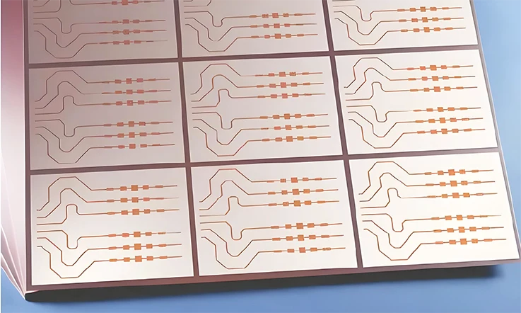
A comprehensive material selection process often involves comparing solutions from different suppliers. Benchmarking RO3035 against key competitors like Taconic and Arlon provides a wider perspective on its position within the high-performance laminate market.
RO3035 vs. Taconic TLY-5 / RF-35
Taconic is a well-regarded supplier of PTFE-based laminates. Their TLY series and RF series are direct competitors to the Rogers RO3000 series.
| Material | Dielectric Constant (Dk) | Dissipation Factor (Df) | Composition |
| RO3035 | 3.50 ± 0.05 | 0.0015 | Ceramic-filled PTFE |
| Taconic TLY-5 | 2.20 | 0.0009 | PTFE |
| Taconic RF-35 | 3.50 | 0.0018 | Ceramic-filled PTFE |
●Electrical Properties: Taconic’s TLY-5 offers a Dk of 2.20, which is significantly lower than RO3035’s 3.50, with an exceptionally low Df of 0.0009. For a closer Dk comparison to RO3035, Taconic’s RF-35 (Dk=3.50, Df=0.0018) is a more direct analog.
●Performance Profile: Compared to Taconic’s RF-35, Rogers RO3035 offers a slightly lower dissipation factor (0.0015 vs. 0.0018), implying marginally better loss performance. Both materials are ceramic-filled PTFE composites and exhibit excellent dimensional stability.
●Selection Rationale: The choice between RO3035 and a Taconic equivalent often comes down to specific application requirements, supply chain availability, and established fabrication expertise with a particular material.
RO3035 vs. Arlon DiClad 880
Arlon, now part of Rogers Corporation but often still considered by its legacy brand name, provides a range of high-performance materials. The DiClad series is based on woven-glass reinforced PTFE.
| Material | Dielectric Constant (Dk) | Dissipation Factor (Df) | Reinforcement Type |
| RO3035 | 3.50 ± 0.05 | 0.0015 | Ceramic-filled (no weave) |
| Arlon DiClad 880 | 2.17 – 2.20 | 0.0009 | Woven-glass PTFE |
●Compositional Difference: RO3035 is a ceramic-filled composite, offering a homogeneous dielectric medium. Arlon DiClad 880 (Dk=2.17-2.20, Df=0.0009) is reinforced with a woven glass fabric. This glass provides mechanical strength but can introduce dielectric anisotropy and the “fiber weave effect.”
●Fiber Weave Effect: In woven-glass materials, a signal trace may pass over areas rich in glass (higher Dk) or areas rich in resin (lower Dk). This can cause localized impedance variations and skew in differential pairs. RO3035’s uniform ceramic filling completely avoids this issue.
●Application Space: For designs that are extremely sensitive to phase accuracy and impedance uniformity at the micro-level, the homogeneous structure of RO3035 presents a distinct advantage.
RO3035 vs. High-Performance FR-4 Alternatives (e.g., Isola IS680)
For cost-driven projects, there is often a temptation to use high-performance epoxy or blended systems instead of PTFE. Isola’s IS680 is one such material.
| Material | Dielectric Constant (Dk) | Dissipation Factor (Df) | Thermal Stability (TCDk) | Material Type |
| RO3035 | 3.50 ± 0.05 | 0.0015 | Excellent (PTFE-based) | Ceramic-filled PTFE |
| Isola IS680 | 3.45 | 0.0035 | Good (epoxy-based class) | Modified epoxy system |
●Loss Tangent Disparity: This is the most significant difference. Isola IS680 has a Dk of 3.45 and a Df of 0.0035. Although this is an outstanding Df for an epoxy-based system, it is still more than double the loss of RO3035 (0.0015). In a high-frequency system, this difference in loss accumulates rapidly.
●Thermal Stability of Dk: While IS680 has good thermal stability for its class, the TCDk of PTFE-based materials like RO3035 is generally superior, meaning its electrical performance will drift less as the device temperature changes.
●Cost vs. Performance Boundary: High-performance FR-4 alternatives are a viable choice for some RF applications. However, for systems where minimal signal degradation is required—such as in mmWave radar or satellite downlinks—the low-loss characteristics of RO3035 are indispensable.
In-Depth Analysis of RO3035 Electrical and Thermal Properties
A granular look at the material’s specifications reveals why it is a preferred substrate for high-fidelity RF circuitry. The stability of its properties under operational stress defines its performance.
Dielectric Constant (Dk) Stability
The dielectric constant dictates the propagation velocity of a signal and is a fundamental variable in impedance calculations. Any variation in Dk can lead to performance degradation.
●Frequency Stability: Unlike FR-4, whose Dk can drop as frequency increases, RO3035 maintains its nominal Dk of 3.50 with very little deviation from DC up to the mmWave range. This allows for broadband designs that perform consistently across their entire operational spectrum.
●Thermal Stability: The thermal coefficient of dielectric constant (TCDk) for RO3035 is exceptionally low, typically around -36 ppm/°C. This means that as the circuit heats up during operation, the dielectric constant remains stable. This prevents thermal drift in filter center frequencies, oscillator phase noise, and antenna matching networks.
Low Dissipation Factor (Df) and Its Impact on Signal Integrity
The dissipation factor, or loss tangent, quantifies how much of a signal’s electromagnetic energy is absorbed by the dielectric material.
●Reduced Insertion Loss: With a Df of 0.0015 at 10 GHz, RO3035 contributes minimally to the overall insertion loss of a transmission line, which is noticeable in designs with long signal paths.
●Sharper Signal Edges: In high-speed digital or pulsed RF applications, a low Df helps preserve the shape of the signal. High loss tends to attenuate the higher-frequency harmonics that constitute sharp digital edges, leading to inter-symbol interference (ISI).
●Lower Thermal Load: In high-power applications, a lower Df means less RF energy is converted to heat within the laminate itself. This reduces the overall thermal load on the system.
Coefficient of Thermal Expansion (CTE) and Structural Reliability
The CTE measures how much a material expands or contracts with temperature. Mismatches in CTE between the laminate and copper can induce mechanical stress.
●X/Y-Axis Stability: The CTE of RO3035 in the X and Y axes is approximately 17 ppm/°C. This value is an excellent match for copper (also ~17 ppm/°C), which minimizes stress on copper traces and solder joints during thermal cycling.
●Z-Axis Stability: The Z-axis (thickness) CTE is also a point of strength, at 24 ppm/°C. This is significantly lower than that of FR-4 (>60 ppm/°C). A low Z-axis CTE ensures the integrity of plated through-holes (PTHs) and vias.
Design and Layout Guidelines for Controlled Impedance with RO3035
Achieving precise controlled impedance is a foundational requirement for nearly all high-frequency PCBs. The consistent properties of RO3035 simplify this task, but best practices in layout remain indispensable.
Microstrip, Stripline, and CPW Trace Calculations
The geometry of a transmission line determines its characteristic impedance.
| Transmission Line Type | Substrate Thickness | Dielectric Constant (Dk) | Target Impedance | Approx. Trace Width |
| Microstrip | 0.508 mm (20 mil) | 3.50 | 50 Ω | ~1.15 mm |
| Stripline | 1.016 mm (40 mil) | 3.50 | 50 Ω | ~0.45 mm |
| Coplanar Waveguide | Variable | 3.50 | Application-specific | Depends on gap and width |
●Microstrip: A trace on an outer layer referenced to an inner-layer ground plane. For a 50 Ω microstrip on a 0.508 mm (20 mil) thick RO3035 substrate (Dk = 3.5), the trace width would be approximately 1.15 mm.
●Stripline: A trace on an inner layer sandwiched between two ground planes. This provides excellent shielding. For a 50 Ω stripline centered in a 1.016 mm (40 mil) total dielectric thickness of RO3035, the trace width would be approximately 0.45 mm.
●Coplanar Waveguide (CPW): A trace flanked by ground planes on the same layer. This structure is often used in mmWave designs for its excellent isolation and ease of integration with on-chip components.
Strategies for Differential Pair Routing and Phase Matching
Differential pairs are used to transmit high-speed signals with improved noise immunity.
●Impedance Control: The differential impedance is a function of trace widths, the spacing between traces (gap), and dielectric properties. For a 100 Ω differential pair on a 0.508 mm RO3035 substrate, a typical geometry might involve 0.5 mm trace widths with a 0.35 mm gap.
●Phase Matching: Any difference in the electrical length of the two traces introduces “skew.” RO3035’s uniform Dk across the board area mitigates “weave skew.” Routing paths should be kept identical in length, with adjustments made using “serpentine” or “trombone” sections.
●Symmetry: Routing should be arranged so that both traces use the same reference plane and keep equal distance from nearby features, maintaining a balanced layout throughout.
Optimizing Multilayer Stackups for Signal Isolation and Symmetry
Multilayer boards are necessary for complex designs, and the stackup architecture is a blueprint for performance.
| Stackup Feature | Recommendation Using RO3035 | Benefit |
| Hybrid Stackup | RO3035 + FR-4 | Cost-efficient high-performance mix |
| Symmetry | Mirror RO3035 & copper layers | Prevents warpage |
| Signal Isolation | Select RO3035 core thickness per signal | Reduces crosstalk between layers |
●Hybrid Stackups: It is common to create hybrid stackups, combining RO3035 with FR-4 to manage costs. In such a design, high-frequency signals are routed on RO3035 layers, while control signals and power planes are on FR-4 layers.
●Symmetrical Construction: A balanced, symmetrical stackup is always recommended to prevent board warpage during lamination and solder reflow cycles. This means mirroring material types and copper weights around the board’s central axis.
●Layer-to-Layer Isolation: For stripline and dual-stripline configurations, the thickness of the RO3035 core material is selected to provide adequate isolation between signal layers, preventing crosstalk.
Advanced Impedance Control: Mitigating Second-Order Effects
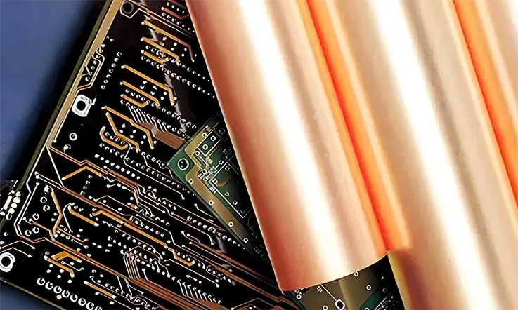
While standard calculations provide a strong baseline, achieving tight tolerances requires accounting for more subtle effects.
The Impact of Copper Roughness on Phase Velocity and Loss
The interface between the dielectric and the copper foil is not perfectly smooth.
●Increased Conductor Loss: At high frequencies, current flows only in a very thin layer on the conductor’s surface (the “skin effect”). A rougher surface increases the effective path length the current must travel, which in turn increases resistive losses. Specifying low-profile (LP) or very-low-profile (VLP) copper can mitigate this.
●Increased Effective Dielectric Constant: The electromagnetic field lines are “slowed down” as they navigate the valleys of the rough copper profile. This makes the signal perceive a slightly higher effective dielectric constant (Dk,eff) than the nominal bulk value of the laminate. Advanced simulation tools can model this effect.
Managing Return Path Discontinuities
A high-frequency signal travels as a loop. Any interruption in its return path creates an impedance discontinuity.
●Via Transitions: When a signal transitions through a via, its return current must also find a path. If the reference planes on the start and end layers are not well-stitched together, the return path becomes long and convoluted. Placing “stitching vias” next to signal vias provides a direct, low-inductance path.
●Gaps in Reference Planes: Routing a high-frequency trace over a split in its reference ground plane is a severe design flaw. The return current is forced to detour around the gap, dramatically increasing the loop inductance and destroying the controlled impedance.
Solder Mask Control and Its Effect on Impedance
For microstrip traces, the solder mask is another dielectric material that influences the final impedance.
●Solder Mask as a Dielectric: The solder mask coating has its own dielectric constant (typically 3.0-3.5) and thickness. When applied over a trace, it effectively creates a multi-dielectric system.
●Impedance Shift: The presence of the solder mask lowers the impedance of the trace compared to the same trace in open air. For the most demanding applications, this effect should be included in impedance simulation models.
Ensuring First-Time Success: Accurate EM Simulation for RO3035
Accurate electromagnetic (EM) simulation is a prerequisite for avoiding costly design spins.
Selecting the Correct Dielectric Constant (Dk): Design vs. Process Values
A common source of error is using an inappropriate Dk value in simulation software.
●Datasheet Dk: This is the nominal value measured under specific test conditions (e.g., at 10 GHz). It’s a good starting point for initial calculations.
●Design Dk / Process Dk: Some suppliers provide application-specific Dk values. A “Design Dk” is often a recommended value for simulation tools. A “Process Dk” might be a value characterized by a specific fabrication house based on their unique lamination and pressing cycles. For the highest accuracy, consulting the fabrication house for their characterized value is the best approach.
Modeling Conductor and Dielectric Losses Accurately
Predicting insertion loss accurately requires modeling all contributing loss mechanisms.
●Conductor Profile: As-fabricated traces have a trapezoidal cross-section due to etching. For fine-line geometries, modeling this trapezoidal shape provides a more accurate calculation of conductor loss than a simple rectangular model.
●Surface Roughness: Copper roughness must be included in the simulation model. Tools like Ansys HFSS and Keysight ADS have built-in models (e.g., Huray snowball, Morgan) that modify the surface impedance of the conductor to account for the increased loss and phase delay caused by roughness.
The Importance of Precise Via Modeling
At frequencies above a few GHz, vias are complex 3D structures with their own parasitic inductance and capacitance.
●Complete Via Structure: An accurate via model must include the via barrel, the capture pad, the clearance (antipad) on the reference planes, and any remaining via stub.
●Stub Effects: The unused portion of a via barrel acts as a resonant stub, creating a deep null in the frequency response. While back-drilling removes this stub physically, it must be accurately represented (or removed) in the simulation to predict performance correctly.
●Via-to-Plane Capacitance: The antipad size determines the capacitance between the via barrel and surrounding ground planes. This capacitance affects the overall impedance of the signal transition.
Fabrication Nuances: A Deep Dive into RO3035 PCB Processing
Fabricating PCBs with PTFE-based materials like RO3035 requires a different set of processes compared to standard FR-4. It demands specialized handling at every stage.
Drilling and Hole Preparation: Techniques for Smear-Free Interconnects
The soft, non-abrasive nature of PTFE presents unique challenges during mechanical drilling.
1.Drilling Parameters:
●Drill Bits: New, sharp, carbide drills with a specific geometry (e.g., 120-140° point angle, high helix) are used to shear the material cleanly rather than tear it.
●Speeds and Feeds: High spindle speeds (RPM) combined with low chip loads (feed rate per revolution) prevent overheating and the smearing of PTFE resin onto the copper layers within the hole barrel.
●Entry/Exit Material: Using rigid entry and exit materials helps to prevent burr formation and ensures the drill starts and exits the hole cleanly.
2.Hole Wall Preparation (Desmearing):
After drilling, the hole walls are not yet ready for plating. The PTFE surface is chemically inert and hydrophobic.
●Plasma Etching: The industry-standard method is a plasma treatment cycle. A mixture of gases (typically Hydrogen and Nitrogen, or sometimes Oxygen/CF4) creates a reactive plasma that etches away any smeared resin and chemically modifies the PTFE surface, creating microscopic texture for plating chemicals to bond to.
●Sodium Naphthenate Etch: An alternative is a chemical process using a sodium naphthalenide solution. This highly reactive chemical strips electrons from the PTFE polymer backbone, creating a carbonaceous, wettable surface. This process is effective but requires stringent handling protocols.
Plating and Surface Activation for PTFE-Based Substrates
Once the hole wall is prepared, the board undergoes a metallization process.
●Direct Metallization: Modern direct metallization processes, which use materials like palladium or graphite, can deposit a conductive layer directly onto the activated hole wall, bypassing the traditional electroless copper bath.
●Electroless Copper: The traditional method involves depositing a thin layer of electroless copper, which acts as the conductive base for the subsequent electrolytic copper plating. The success of this step is entirely dependent on the quality of the preceding desmear stage.
●Panel vs. Pattern Plating: Both processes are applicable. Pattern plating, where copper is plated only on the desired circuit features, is often preferred for fine-line RF designs as it offers better control over trace geometry.
Lamination Cycles: Pressure, Temperature, and Material Compatibility
When creating multilayer boards, the layers are bonded together in a lamination press.
●Bonding Materials: RO3035 layers are typically bonded using compatible, low-loss bonding films like Rogers 3001 or other thermoplastic prepregs. Using a standard FR-4 prepreg would result in delamination.
1.Lamination Profile:
●Temperature: The lamination temperature must be high enough for the bonding film to flow properly, typically in the 200–220°C range.
●Pressure: Pressure must be carefully controlled. Excessive pressure can cause the soft PTFE material to deform or “flow,” leading to variations in layer thickness.
●Ramp Rates: Slow, controlled temperature ramp rates (both heating and cooling) are used to prevent thermal shock and to minimize internal stresses that could lead to warpage.
Assess Your Design’s Manufacturability The transition from design to fabrication for RO3035 involves specialized equipment and validated process controls. Submit your Gerber files for a complimentary manufacturability review to identify potential challenges before production.
Quality Assurance and Reliability Testing for RO3035 Assemblies
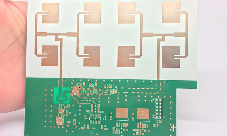
Verifying that a finished PCB meets its design intent requires a suite of specialized tests beyond simple continuity checks.
Time Domain Reflectometry (TDR) for Impedance Verification
TDR is a fundamental tool for verifying controlled impedance.
●How it Works: A TDR instrument sends a very fast-rise-time pulse down a transmission line. Any changes in impedance cause reflections, which are captured and displayed as an impedance profile versus electrical distance.
●What it Finds: This test immediately reveals if the trace impedance is within its specified tolerance (e.g., 50 Ω ± 10%). It can pinpoint the exact location of impedance discontinuities caused by manufacturing variations, incorrect trace geometry, or connector launches. TDR testing is typically performed on test coupons fabricated on the same panel as the main boards.
Vector Network Analyzer (VNA) for S-Parameter Characterization
A VNA provides a complete picture of a circuit’s RF performance by measuring its scattering parameters (S-parameters).
●Insertion Loss (S21): This measures how much signal is lost as it passes through the device under test. For RO3035 boards, this measurement validates that the low-loss properties of the material have been preserved through fabrication.
●Return Loss (S11): This measures how much signal is reflected back towards the source due to impedance mismatches. A good return loss (a large negative number in dB) indicates a well-matched circuit.
●Crosstalk (S31 or S41): In dense circuits, a VNA can be used to measure the unwanted coupling of energy from one trace to an adjacent one, verifying that the layout provides sufficient isolation.
Thermal Shock and Cycling Tests for Durability Assessment
These tests simulate the environmental stresses a board will experience over its lifetime.
●Procedure: Boards or test coupons are subjected to rapid transitions between extreme hot and cold temperatures (e.g., -40°C to +125°C) for hundreds or thousands of cycles.
●Purpose: This accelerates aging and exposes weaknesses. For RO3035 boards, this is a test of PTH and microvia reliability. The excellent CTE match of RO3035 to copper means it performs exceptionally well in these tests.
Conductive Anodic Filament (CAF) Resistance Testing in Hybrid Builds
CAF is an electrochemical migration failure mode that can lead to short circuits between adjacent conductors.
●Relevance: This test is especially relevant for hybrid stackups where RO3035 is combined with glass-reinforced materials like FR-4. The interface between different materials can be a pathway for CAF formation under conditions of high humidity, temperature, and voltage bias.
●Testing: A test coupon with a specific pattern of closely spaced vias is subjected to these harsh conditions, and the resistance between them is monitored over time. A drop in resistance indicates the onset of CAF failure.
Client Testimonial: “For our application, consistency from board-to-board is everything. The supplied TDR and S-parameter test data for each lot provided the documentation needed for our system-level validation, accelerating our integration schedule significantly.” — Senior Hardware Engineer, Aerospace & Defense Contractor.
Troubleshooting RO3035 Circuits: From Lab to Product
Even with meticulous design and fabrication, high-frequency circuits can exhibit unexpected behavior. A systematic approach to troubleshooting can quickly isolate the root cause.
Troubleshooting Higher-Than-Expected Insertion Loss
●Symptoms: The measured signal attenuation (S21) through a trace or component is worse than simulated.
●Possible Causes:
1.Connector Launch: Poor solder joints at the RF connector interface are a common source of loss and reflection.
2.Etching Variation: If traces are etched narrower than designed, their resistive loss increases.
3.Copper Surface Roughness: The actual copper roughness may be greater than what was modeled.
●Diagnostic Steps:
1.Use a VNA with gating/TDR functionality to isolate losses at each connector launch versus the loss of the trace itself.
2.Perform a physical cross-section analysis on a sacrificial board or test coupon to measure the final trace geometry.
Diagnosing Impedance Mismatches and Reflections
●Symptoms: The measured return loss (S11) is poor. A TDR measurement shows deviations from the target impedance.
●Possible Causes:
1.Dk Value Mismatch: The actual processed Dk of the board differs from the value used for impedance calculations.
2.Return Path Discontinuity: The signal trace passes over a gap in its reference ground plane, or a via transition lacks a nearby return via.
3.Via Stub Resonance: An un-removed via stub creates a resonant structure that acts as a notch filter at a specific frequency.
●Diagnostic Steps:
1.A TDR is the primary tool. It will show the impedance profile along the trace, pinpointing the physical location of the mismatch.
2.Correlate the location of the impedance deviation on the TDR plot with the PCB layout file to identify the offending feature.
Investigating Filter or Resonator Frequency Shifts
●Symptoms: The center frequency of a filter or the resonant frequency of an antenna element is shifted from the designed value.
●Possible Causes:
1.Effective Dk Variation: The most likely cause. The final processed Dk of the laminate is slightly different from the value used in the simulation.
2.Etching Offsets: The physical dimensions of the resonant structures were altered during the copper etching process.
●Diagnostic Steps:
1.Fabricate a simple, well-characterized resonant structure (e.g., a ring resonator) on the same manufacturing panel as a test coupon.
2.By measuring the resonant frequencies of this coupon, one can back-calculate the precise effective Dk of that manufacturing batch.
Advanced Applications and Miniaturization with RO3035
The trend towards smaller electronic devices places stringent demands on PCB substrates. RO3035’s properties make it an enabler for high-density, miniaturized RF modules.
High-Density Interconnect (HDI) and Microvia Integration
●Microvia Compatibility: RO3035’s homogenous, non-reinforced composition performs well during laser drilling. The material ablates efficiently, producing smooth-walled microvias that support dependable plating results.
●Stacked and Staggered Vias: The material’s mechanical stability supports advanced HDI structures like stacked microvias and via-in-pad designs, allowing for extremely compact routing.
●Reliability: The low Z-axis CTE of RO3035 ensures the long-term reliability of these microvia structures, even when subjected to thermal stresses.
Utilizing Thin-Core RO3035 for Miniaturized Modules
●Reduced Stackup Height: Using thin cores (e.g., 0.127 mm) directly reduces the overall thickness of the final PCB, a primary requirement for space-constrained applications.
●Finer Line Geometries: Thinner dielectrics allow for narrower trace widths to achieve a given impedance, enabling finer-pitch routing.
●Improved Thermal Performance: In some configurations, thinner dielectrics can reduce the thermal path from active components on the surface to a ground or thermal plane, aiding in heat dissipation.
Suitability for Wearable and Implantable RF Devices
●Low Moisture Absorption: RO3035’s hydrophobic nature is a significant advantage. It resists absorbing moisture from the body or the environment, ensuring its electrical properties remain stable.
●Mechanical Compliance: The material’s PTFE base provides a degree of compliance that can be beneficial in rigid-flex designs, which are common in wearable electronics.
●Biocompatibility Considerations: While RO3035 itself is not pre-certified as biocompatible, its inert chemical nature (PTFE) makes it a suitable candidate for use within medical devices, typically encapsulated with a certified biocompatible coating.
Navigating High-Power and Millimeter-Wave Designs with RO3035
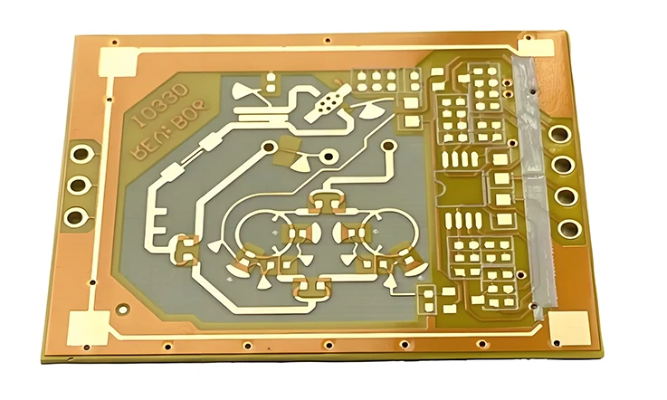
As applications push into higher power domains and mmWave frequencies, the choice of laminate becomes even more influential.
Thermal Management in High-Power Amplifier (HPA) Designs
●Thermal Conductivity: RO3035 has a thermal conductivity of 0.5 W/m·K. While not as high as metal-core PCBs, this is superior to many standard FR-4 materials and facilitates the spreading of heat.
●High-Temperature Stability: The material’s PTFE structure remains stable at temperatures well above 280°C. It will not soften or undergo significant changes in mechanical properties during high-temperature operation.
●Heat Spreading with Copper: The layout can be designed to leverage copper planes as heat spreaders. By connecting the thermal pads of power devices to large ground planes through an array of thermal vias, heat can be efficiently conducted away.
Performance in 77 GHz Automotive Radar and mmWave Systems
●Extremely Low Loss: At 77 GHz, the dissipation factor of RO3035 remains remarkably low (typically ~0.0019). This is necessary for radar systems, where signal loss directly translates to reduced detection range.
●Propagation Consistency: The stable and uniform dielectric constant is perhaps its most valuable attribute here. It ensures that the phase relationships in complex antenna arrays are precisely maintained.
●Surface Finish: RO3035 is available with very smooth electrodeposited (ED) copper, minimizing the additional conductor loss factor caused by the skin effect at mmWave frequencies.
Achieving Low Passive Intermodulation (PIM) in Base Station Antennas
●Material Homogeneity: RO3035’s uniform composition of ceramic and PTFE minimizes sources of non-linearity. The interface between glass fibers and resin in some materials can be a source of micro-level PIM generation.
●Stable Copper Adhesion: The adhesion between the copper and PTFE substrate remains steady and uniform under thermal stress, reducing the risk of micro-cracks or fluctuations in contact resistance.
●Current Distribution: The material’s stable dielectric behavior supports even spreading of RF currents across conductor surfaces, helping to prevent localized current buildup at “hot spots” that may intensify non-linear responses.
Cost-Benefit Analysis and Optimization Strategies
While RO3035 is a premium performance material, its use does not have to result in an unmanageable budget. Strategic choices can yield a cost-effective solution.
Strategic Use of Hybrid Stackups
●Concept: This involves using RO3035 only for the layers carrying high-frequency signals and using a lower-cost material like FR-4 for the core, which may contain only DC power or low-speed control signals.
●Implementation: This requires careful design to manage the interface between the different materials and a fabrication process capable of bonding them reliably.
●Benefit: This approach localizes the high cost of the RF laminate only where it is electrically necessary, reducing the overall raw material cost.
Maximizing Panelization Efficiency
●Panel Utilization: A fabricator’s standard panel size is fixed (e.g., 18×24 inches). The unit cost of a board decreases as more instances of that board can be arrayed onto a single panel.
●Design for Manufacturability (DFM): Minor adjustments to a board’s dimensions during the layout phase can have a large impact. Reducing a board’s length by a few millimeters might allow an extra row of boards to fit on the panel, lowering the per-unit price.
Evaluating the Cost Impact of Process Complexity
●Feature Trade-offs:
1.Standard plated-through holes are less expensive than laser-drilled microvias.
2.Standard trace widths and spacings are less costly to produce than fine-line features.
3.Back-drilling adds a process step and cost, but may be cheaper than moving to a thinner, more expensive laminate to achieve the same signal integrity.
●Informed Decisions: By understanding these trade-offs, a design can be optimized to meet performance targets without “over-engineering” features that add substantial cost for marginal gain.
Request a Custom Stack-up Proposal Balancing performance and budget often begins with the right material stack-up. Describe your project requirements to receive a custom hybrid stack-up proposal tailored to your application’s needs.
Key Checklist for RO3035 PCB Design & Fabrication
This checklist serves as a practical guide to translate the material’s benefits into a successful final product.
1. Design Phase Checklist
●Impedance Modeling: Have simulation models been adjusted for copper surface roughness effects on effective dielectric constant and conductor loss?
●Return Path Integrity: Is there a continuous ground reference under every high-frequency trace? Have all via transitions been analyzed to ensure a short return current path?
●Differential Pair Routing: Are traces within each pair routed with tight physical symmetry and length matching?
●Stackup Symmetry: For multilayer boards, particularly hybrid constructions, is the stackup designed to be symmetrical to mitigate warpage?
●Solder Mask Impact: Has the impedance-lowering effect of solder mask on outer-layer traces been considered?
2. Fabrication File & Notes Checklist
●Hole-Wall Preparation: Does the fabrication drawing explicitly mandate a specific hole-wall activation process suitable for PTFE, such as a plasma etch cycle?
●Copper Foil Specification: Is the desired copper foil type (e.g., standard ED, Low Profile, VLP) clearly specified?
●Bonding Material for Multilayers: Is the compatible bonding material (e.g., Rogers 3001 bonding film) explicitly called out in the stackup notes?
●Controlled Impedance Callouts: Are all controlled-impedance traces identified, with their target impedance and tolerance specified?
●Back-Drilling Requirements: If back-drilling is required, are the specific vias, target depth, and remaining stub tolerance clearly documented?
Application Snapshots: From Concept to Reality
Theoretical knowledge is best illustrated by real-world application. The following anonymized summaries demonstrate how the properties of RO3035 are leveraged to solve tangible engineering problems.
Snapshot 1: Automotive Radar Front-End
●Project Sector: 77 GHz Automotive Radar
●Challenge: Achieving stringent phase matching (<1° variance) across a large phased-array antenna to ensure beamforming accuracy, while managing thermal loads from integrated MMICs.
●Solution & Outcome: A hybrid stack-up was constructed using a 5 mil RO3035 core with VLP copper for the RF sections and an FR-4 core for control circuitry. Precision back-drilling and tightly managed etching were applied, delivering stable phase behavior and dependable thermal behavior across the full range of automotive temperature conditions.
Snapshot 2: Satellite Communications LNB
●Project Sector: Ka-Band LNB (Low-Noise Block) Downconverter
●Challenge: Minimizing insertion loss in the input filter and feed network to maximize the system’s G/T figure of merit. The design required extremely tight impedance control of 50Ω ±2%.
●Solution & Outcome: A pure RO3035 build with a smooth copper profile was selected. TDR verification on every panel’s test coupon confirmed impedance was held within ±1.5%. The final assembly exceeded the target G/T performance metric, attributed directly to the ultra-low loss characteristics of the substrate.
Snapshot 3: 5G Power Amplifier
●Project Sector: High-Power GaN Doherty Amplifier for 5G Base Station
●Challenge: Ensuring long-term reliability of solder joints and plated-through holes under intense thermal cycling generated by the GaN-on-SiC power transistors.
●Solution & Outcome: The low X/Y-axis CTE of RO3035, closely matched to copper, minimized thermomechanical stress on all interconnects. A dense array of thermal vias, validated by cross-section analysis, effectively wicked heat away from the device junction, enabling the final product to pass over 2000 thermal shock cycles (-40°C to +125°C) without failure.
Bridging Design and Reality: Fabrication and Service Capabilities
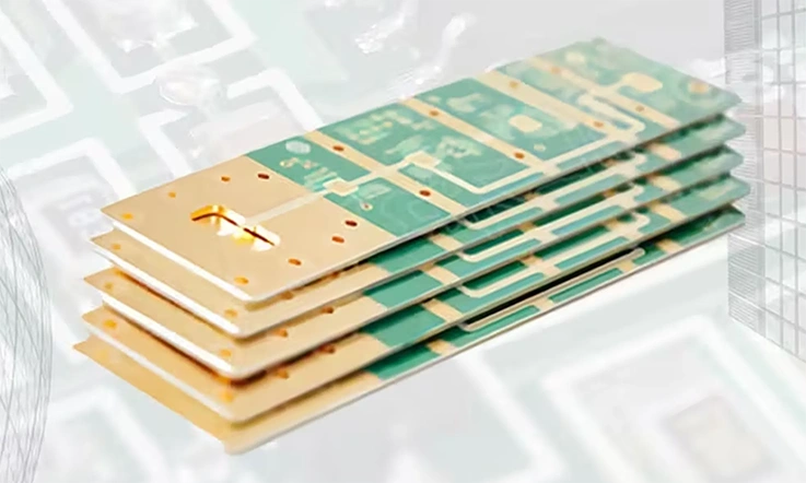
A successful high-frequency project depends not only on superior material selection but also on the fabrication expertise that translates a complex design into a flawless physical product. The following outlines the core capabilities available to support your most demanding Rogers PCB applications.
Advanced Rogers PCB Manufacturing Technology
Precision in high-frequency PCB fabrication is non-negotiable. The manufacturing process is supported by a suite of specialized technologies calibrated for the unique properties of Rogers materials:
●Plasma Etching & Hole-Wall Activation: In-house plasma treatment systems to perform the essential desmear and surface activation of PTFE, ensuring robust via plating adhesion and long-term interconnect reliability.
●Controlled-Depth Back-Drilling: Precision back-drilling capabilities to remove resonant via stubs, significantly improving signal integrity in high-speed and high-frequency channels.
●Laser Direct Imaging (LDI): LDI technology is applied to accurately define fine-line traces and spaces, enabling dense layouts required for mmWave and high-speed digital applications.
●Hybrid Multilayer Lamination: Extensive experience in bonding Rogers PTFE-based materials with dissimilar materials like FR-4 in complex, reliable hybrid stack-ups.
●Specialized AOI & RF Testing: Automated Optical Inspection (AOI) systems configured for RF structures, complemented by VNA and TDR testing capabilities for full S-parameter and impedance characterization.
Cost-Effective Solutions and Competitive Pricing
Performance does not have to come at an unmanageable cost. A strategic approach to pricing and cost optimization is employed:
●Strategic Material Sourcing: Established supply chain relationships allow for competitive procurement of authentic Rogers laminates and bonding materials.
●Complimentary DFM/DFA Review: A thorough Design for Manufacturability (DFM) and Assembly (DFA) analysis is provided on all engineering files, identifying and rectifying costly design flaws before fabrication begins.
●Panelization Optimization: Intelligent board array design on production panels minimizes material waste, directly lowering the per-unit cost for both prototype and volume orders.
Expedited Lead Times and Reliable Delivery
Amid rapid development timelines, both rapid turnaround and dependable outcomes matter. The process is designed with streamlined execution in mind:
●Quick-Turn Prototyping: Dedicated processes for rapid prototyping of Rogers PCB projects, enabling faster design validation and iteration.
●Streamlined Quoting & Engineering: An efficient front-end process ensures that quotes are delivered promptly and engineering questions are resolved without delay, moving projects into fabrication faster.
●Transparent Project Tracking: Proactive communication and access to real-time status updates provide full visibility into the project’s progress from order to shipment.
Dedicated Engineering and Technical Support
Navigating the complexities of RF design requires a collaborative approach. A support structure is in place to function as an extension of your engineering department:
●Expert Consultation: Direct access to engineering personnel with deep experience in RF and high-speed PCB fabrication for stack-up design, material selection, and impedance modeling inquiries.
●Single Point of Contact: Each project is supported by a designated technical contact who facilitates smooth, reliable, and well-informed communication from start to finish.
●Design Intent Preservation: The focus is on a collaborative partnership to ensure that the final fabricated board perfectly mirrors the original design’s performance intent.
Client Testimonial: “The DFM feedback on our hybrid stack-up was invaluable. The suggestion to adjust the layer transition saved us what would have been a costly full design spin. The engineering dialogue was a genuine extension of our own design process.” — Lead RF Engineer, Satellite Communications Firm.
In a Word: The Strategic Value of RO3035
Rogers RO3035 laminate is an enabling technology for a wide range of advanced RF and microwave systems. Its value lies in its exceptional stability. The stable dielectric constant, very low dissipation factor, and mechanically robust CTE profile provide a predictable foundation for circuits where performance is a primary objective. From the precision required for 77 GHz automotive radar to the low-loss demands of satellite communication links and the structural integrity needed for high-power amplifiers, RO3035 directly addresses the primary challenges in modern high-frequency design. Its fabrication requires specialized knowledge, and the resulting performance and reliability justify its selection in applications that define the cutting edge of electronic technology.
H2:Frequently Asked Questions (FAQ)
1.What is the typical surface roughness of the copper on Rogers RO3035?
Surface roughness varies with the copper foil type, ranging from ~5 µm for standard ED copper to as low as ~1.5 µm for Very Low Profile (VLP) copper. For millimeter-wave applications, smoother VLP copper is recommended to reduce conductor loss.
2.Can RO3035 be used in a rigid-flex PCB design?
Yes. RO3035 is frequently used for the rigid sections of rigid-flex PCBs. Success depends on using a compatible bonding adhesive (bondply) that can withstand the necessary lamination temperatures without damaging the flexible core.
3.What is a primary cause of failure during RO3035 board fabrication?
A common fabrication failure is improper hole-wall preparation before plating. The inert PTFE surface requires a specialized activation process, like plasma etching, to ensure strong copper adhesion. Without it, via plating may fail, leading to open circuits.
3.How does the dielectric constant of RO3035 change with temperature?
RO3035’s dielectric constant is exceptionally stable. Its Thermal Coefficient of Dielectric Constant (TCDk) is very low, at approximately -36 ppm/°C, ensuring minimal performance drift in environments with fluctuating temperatures.
4.Is back-drilling of vias recommended for RO3035 boards?
Yes, back-drilling is highly recommended for high-frequency signal paths on RO3035 boards. This process removes the unused portion (stub) of a via, eliminating signal reflections and resonance issues that degrade signal integrity.
Our services
Rogers PCB Laminates & Series

