As a PCB designer, it is important to acknowledge that the manufacturing of IoT devices necessitates a specialized breed of circuit boards that pose unique design and manufacturing challenges. Unlike conventional electronic products, IoT devices push the boundaries of manufacturers and designs. Manufacturers have been facing difficulties keeping up with the rapid-scale adoption of new technologies in the market, further complicating the manufacturing processes involved.
The design and integration of IoT components into circuit boards require strict adherence to design rules and complex component integration, with the additional challenge of constantly evolving technology. Manufacturers must continually adapt to new technological advancements to remain competitive, which can prove to be a significant challenge. This has led to the slow adoption of IoT technology by companies and organizations, with more than half of them finding it challenging to implement.
However, despite these challenges, the production and sale of IoT devices continue to increase substantially due to market demands. As a PCB designer, it is imperative to understand the effects of IoT on PCB manufacturing to ensure the successful implementation of IoT projects.
What Is IoT ?
The emergence of the Internet of Things (IoT) marks a convergence between the physical and digital domains, where devices other than personal computers can connect to IP networks. While smartphones represent the most prominent examples of IoT, recent advancements, such as the proliferation of apps for running household appliances and utilities, the advent of wearable technology, and vehicles equipped with data accessibility, underscore the boundless potential of IoT.
Despite consumer electronics being the first to come to mind when thinking of IoT, industries such as manufacturing, transportation, and healthcare surpass personal electronics and automobiles in leveraging the transformative potential of the IoT revolution. Therefore, these large-scale industries require PCB designs that are innovative, confer flexibility, and deliver high-speed connectivity to enable globally optimized operations.
Advantages of (Internet of Things) IoT
● Enhanced Connectivity: IoT provides seamless and smart connectivity between devices, enabling the exchange of real-time data, and improving operational efficiency.
● Improved Efficiency: IoT streamlines processes, automates tasks, and optimizes resource utilization for enhanced productivity and reduced costs.
● Greater Insights: IoT-generated data offers new insights into complex systems and user behaviors, allowing for better decision-making, improved user experience, and new opportunities for innovation.
● Enhanced Safety and Security: IoT devices can enhance safety measures by monitoring and identifying potential hazards while also maintaining security through secure encryption protocols.
● Increased Revenue: IoT improves product performance, service delivery, customer engagement, and support services, all of which contribute to increased revenue.
● Cost Reduction: IoT can provide significant cost reductions in areas such as energy consumption, inventory management, maintenance, and supply chain optimization.
So, we can think that IoT offers a broad range of advantages, ushering in opportunities for innovation, automation, and enhanced productivity across various industries.
Disadvantages of (Internet of Things) IoT
While the Internet of Things (IoT) brings many benefits, it also presents certain challenges and disadvantages, which include:
● Security Risk: IoT devices can be vulnerable to cyber-attacks, and as a result, data privacy and security can become major concerns.
● Complexity: IoT devices can be complex and require specialized skills in design, development, and implementation. This can result in higher development costs, reduced interoperability, and integration challenges.
● Interoperability: The lack of standardization in IoT devices and platforms can make interoperability difficult, limiting their effectiveness and creating fragmentation in the market.
● Accessibility and Reliability: IoT devices rely heavily on connectivity and network accessibility, which can be limited or disrupted by various factors such as geographic location, network issues, or power outages.
● Data Overload and Management: With the abundance of data generated by IoT devices, weakness in data collection, analysis, and processing of large sets of data can become a challenge, overwhelming systems and impacting efficiency.
● Ethical Issues: IoT raises several ethical concerns such as far-reaching data collection capabilities, privacy, and security threats, and the potential bias and responsibility associated with automated decision-making.
Therefore, while IoT offers numerous benefits, measures are required to address the challenges that arise in its implementation, safeguard data privacy, address reliability issues, and standardize processes to allow for proper operation and integration.
What Is PCB in IoT ?
The Internet of Things (IoT) refers to a network of various electronic devices that are specifically designed to communicate with each other through internet connectivity, employing software, sensors, and other technologies in their creation. An example of IoT in action is the connection of a smartphone to a refrigerator to utilize a smartphone app that enables users to examine its contents remotely. Using this technology, individuals can remotely monitor their homes by connecting their phones to CCTV cameras and even shop for needed items while away from home, while still keeping track of their refrigerator’s contents.
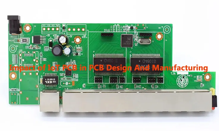
IoT Printed Circuit Boards (PCBs) provide power to IoT hardware, serving as the foundation or fundamental structure upon which these devices are built. Given the congestion of RF bandwidth by high-frequency IoT applications, unwanted meddling and safety issues may arise. Accordingly, PCB designers must shield all sensitive electronics to reduce hazards from EMI, while an efficient grounding mechanism provides protection against interference issues. In summary, IoT PCB design is essential for safety and health reasons
PCB Design Requirements for the Internet of Things
The emergence of IoT technology has brought about unprecedented challenges in PCB design engineering. Designers are now required to consider issues that were not previously encountered, such as evaluating consumer interaction with everyday items that have been equipped with IoT functionality. This represents a shift in focus from how users interact with electronic devices to assessing how they engage with traditionally non-tech items. Consequently, the PCB design process is changing, with an increased emphasis on reliability and minimal assembly errors. This is particularly crucial given the steadily growing demand for household products equipped with IoT features. PCB design engineers must strive to meet these challenges by incorporating high-quality standards into their work and continually adapting to new trends in the IoT.
The Changes in the IoT PCB Design Process
The process of developing IoT-optimized products involves a series of critical phases, beginning with an evaluation of potential new form factors, followed by the selection of appropriate PCB materials and layouts. Throughout the product design flow, it is essential to consider the requirements for assembly into a completed product.
One of the most significant impacts of IoT is the blurring of the lines between mechanical and electronic aspects, as well as between the product itself and its PCB form. Collaboration between PCB designers, mechanical designers, and electrical engineers throughout the entire design process has become increasingly relevant, representing a departure from previous assembly line-like procedures. As such, teamwork and cross-functional communication have become essential elements in creating successful IoT products. By working collaboratively, the team can ensure that the PCB design is seamlessly integrated with the mechanical and electronic aspects, resulting in a high-quality, functional product that meets the needs of consumers.
IoT PCB Design Tips and Recommendations
When it comes to designing a PCB for optimal IoT performance, several key design areas require special attention. As a PCB design engineer, it is crucial to keep these elements in mind and implement strategies that ensure a flawless design. Below are some critical design areas and tips for enhancing the quality of your IoT PCB design:
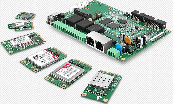
● Wireless Connectivity: Incorporating internet connectivity into an Internet of Things (IoT) printed circuit board (PCB) is pivotal to its functionality. Consequently, selecting suitable wireless modules and RF circuit components is paramount in the data collection and transmission process. As a PCB design engineer, it’s essential to bear in mind power consumption, network range and speeds, as well as security requirements when determining the most appropriate components for your design.
● Power Consumption: IoT devices must consume minimal power to ensure long battery life and optimal performance. Utilize low-power components, and consider implementing power-saving features such as sleep modes to minimize power consumption.
● Connectivity: Strong and reliable data connection is a critical aspect of IoT devices. Ensure that your PCB design includes antenna components with adequate range and bandwidth. Proper placement of wireless modules can also enhance signal strength.
● EMI/RFI: Electromagnetic interference (EMI) and radio-frequency interference (RFI) can compromise IoT device performance. Proper grounding, power management, and isolation techniques can prevent EMI and RFI and ensure the device operates reliably.
● Sensor Integration: IoT devices rely on sensors to collect and transmit data. Ensure that you have selected the appropriate sensors for your device, and that they are correctly placed, secured, and interlinked.
● Form Factor: IoT devices come in various forms, including wearables, home appliances, and industrial equipment. Ensure that your PCB design is optimized for the specific form factor, taking into account factors such as size, weight, and interface.
● Product Fitting: In PCB design, it’s crucial to consider not only the physical size of the board but also ensuring the shape of the design can be seamlessly integrated into the intended IoT form. Due to the non-traditional materials commonly used in IoT products, such as mesh or plastic components, circuit layout often needs to adapt to ensure optimal functionality. Effective virtual prototyping is essential to verify that the design can effectively accommodate any necessary modifications to meet the product’s requirements.
● Reliability Standards: As technology continues to evolve, so do the standards for ensuring the trustworthiness of electronic devices. In the case of flexible circuit boards, designers must adhere to specific guidelines to prevent their boards from cracking under varying stresses and environmental changes, thus ensuring their reliability. Consumers expect electronic devices to operate accurately and reliably for extended periods. Therefore, designers are under significant pressure to create products that can withstand a range of potential conditions. To achieve this, many designers turn to simulation software to test their designs thoroughly.
By taking into account these important design areas, you can strengthen your IoT PCB design and create high-performance, reliable IoT devices that are sure to meet the demands of today’s tech-savvy world.
Challenges of Integrating IoT devices in PCB Design
Integrating IoT devices in PCB design can present several challenges, including:
Power management: IoT devices typically operate on limited power sources, such as batteries. PCB designers must carefully manage power consumption to ensure that IoT devices can operate efficiently without draining their power sources too quickly.
Size and space constraints: IoT devices are often smaller than traditional components, requiring PCB designers to incorporate miniature components that can be challenging to work with. This also poses challenges when it comes to layout and routing of the components, especially when dealing with high-density designs.
Connectivity protocols: IoT devices use a variety of connectivity protocols, including Wi-Fi, Bluetooth, Zigbee, and cellular networks. PCB designers must ensure that their designs are compatible with the chosen protocol and that they can handle the specific requirements of each protocol.
Security: IoT devices pose significant security risks, and PCB designers must incorporate robust security features into their designs to ensure data privacy and prevent hacking and other cyber threats.
Testing: IoT devices and sensors can be complex, and testing them can be challenging. PCB designers must ensure that their designs can be adequately tested to verify that they meet performance requirements and can integrate seamlessly into the larger system.
PCB Design Considerations for Manufacturing IoT Devices
The design of a PCB for IoT devices requires a comprehensive strategy that takes into account several critical considerations, such as security, interoperability, power/processing capabilities, scalability, availability, controllability, and the operational environments. IoT devices can be deployed in various settings, including consumer, industrial, or enterprise environments. To ensure the smooth and efficient manufacture of IoT devices, PCB design engineers must determine the specific device type and classification and address any design considerations and Design for Manufacturability (DFM) concerns accordingly. This requires close collaboration with Contract Manufacturers (CMs). Below is a list of essential PCB design considerations and DFM concerns categorized by IoT device type and classification.
| Device Class (Devices) | PCB Design Considerations | DFM Concerns |
| Consumer(home appliances, wearables, smart TVs) | Board flexibilityboard size, EMI, signal integrity, high density interconnect (HDI) | Component placement, trace lengths, stackup, via types, connector constraints, bend radii |
| Industrial(pumps, motors, ID tags) | Board strength, thermal capacity, high voltage, integration with mechanical design | Board material, trace sizes, thermal reliefs |
| Enterprise(computing equipment, security systems, temperature control) | Power reliability, connectivity, RF, high frequencies, module connectivity | Depanelization, component placement, trace lengths, radiation |
While it’s critical to prioritize the key PCB design considerations mentioned earlier, it’s important not to overlook other factors that could impact the DFM. PCB design engineers must ensure that their DFM takes into account the capabilities and manufacturing equipment of their Contract Manufacturers (CMs). This ensures that the PCB design meets the essential requirements of manufacturing IoT devices effectively. Adequate attention to both fundamental and nuanced design considerations allows the successful creation of IoT devices that meet the necessary standards for reliable and effective performance.
IoT in relation to PCB design and manufacturing
The advent of IoT has significantly impacted PCB design and manufacturing as it necessitates the integration of wireless communication capabilities into numerous smart objects flooding the market. The incorporation of RF technology components into a product imposes stringent design rules on the entire system, including the Printed Circuit Board, and mandates the execution of specific testing and validation processes at the end of the manufacturing process.
The addition of one or more chips dedicated to wireless connectivity for diverse applications, including industrial sensors, wearable devices, and location trackers, presents significant design challenges for the product design team. As such, PCB design engineers must be proficient in addressing these challenges, including selecting appropriate components, adhering to design rules, and effectively integrating wireless capabilities into products, to produce reliable and sustainable IoT devices.
● Integration: PCB design engineers face significant challenges when integrating wireless communication capabilities into the compact form factor of IoT devices. This requires the careful selection and placement of additional components, making efficient use of available space within the device.
● RF Design: Designing a product with embedded RF communication capabilities necessitates the adherence to stringent design rules aimed at optimizing the radio performance while minimizing interference with other components and systems. Moreover, it is crucial to comply with relevant regulations and standards concerning RF pollution, power transmission, and other related issues. PCB design engineers should demonstrate proficiency in RF design techniques to ensure that IoT devices operate effectively and efficiently without interfering with other systems or breaching regulatory provisions.
This impacts the PCB routing as well:
When designing RF circuits, it is crucial for PCB design engineers to consider impedance matching during signal routing. The absence of impedance matching leads to substantial power losses, as well as hazardous signal reflections along the PCB traces. As many systems and RF modules have a standard impedance of 50 Ω, it is advisable for RF PCB traces to have an identical characteristic impedance. Microstrips and striplines are two frequently used trace types on PCBs, with the latter particularly useful in 4-layer PCBs for improved routing.
Apart from stack-ups, the designer must ensure that RF signals are suitably isolated to regulate unwanted coupling with other signals. The customary method is to use a continuous ground plane situated immediately below the upper layer with components and transmission lines. The design team must also pay attention to shielding to avoid interference between the RF circuitry and the baseband section.
The PCB and product assembly processes are subject to strict requirements when designing RF circuits. Additionally, testing processes are a critical aspect that will most likely require RF testers on the line. By addressing these considerations, PCB design engineers can ensure optimal design, manufacturing, and testing of RF circuits in IoT devices.
Importance of IoT in PCB design and manufacturing
IoT (Internet of Things) has emerged as a critical technology for the world of electronics and has revolutionized PCB (Printed Circuit Board) design and manufacturing. Here are some of the key reasons for why IoT is important in PCB design and manufacturing:
● Smart Connectivity: IoT devices have sensors that allow them to connect and communicate with other devices over the internet. With IoT, PCB designers can incorporate smart connectivity features into their designs, which creates a more connected and efficient system.
● Enhanced Product Functionality: IoT technology enables PCB designers to add a wide range of functionalities to their designs. With IoT, PCBs can be designed to perform complex tasks such as monitoring environmental conditions, tracking location, and controlling other devices.
● Improved Reliability: IoT technology makes it possible for PCB manufacturers to build more reliable and robust systems. With IoT, devices can monitor and report data to help identify any potential issues before they become critical failures.
● Higher Efficiency: IoT devices and sensors can collect and analyze data, allowing for more efficient processes and optimized performance. This data can then be used by PCB designers to create more efficient systems, reducing costs and improving overall performance.
● New Market Opportunities: IoT has opened up new markets for PCB manufacturers, creating opportunities for businesses to develop new products and services that can take advantage of the connectivity and functionality of IoT devices.
Impact of IoT on PCB Industry
IoT has had a significant impact on the PCB industry, including:
● Increased demand for smart connectivity: The rise of IoT has led to an increased demand for smart connectivity in PCB designs. This has led to the development of new technologies and components that can enable this connectivity.
● Adoption of new materials: PCB designers are adopting new materials and substrates that can support the high data rates and high-frequency requirements of IoT devices.
● Greater design complexity and miniaturization: IoT devices are often smaller and more complex than traditional electronics, leading to greater design complexity and miniaturization in PCBs.
● New testing and validation requirements: IoT devices require more stringent testing and validation, including testing for wireless connectivity and power efficiency.
● Increased collaboration between manufacturers and designers: IoT devices require close collaboration between manufacturers and designers to ensure the seamless integration of hardware and software components.
Therefore, IoT has led to new innovations and opportunities in the PCB industry, leading to higher performance, increased connectivity, and improved user experiences.
The Future of PCB Design for the IoT
● The fast-growing IoT industry has raised questions regarding whether PCB design for IoT will become increasingly individualized or standardized. Despite every IoT device having unique characteristics, there are common requirements that suggest a growing trend towards mixing and matching the same design protocols repeatedly.
● IoT presents immense opportunities and challenges for the PCB industry, and its growth is expected to continue. This trend has the potential to blur the lines between electrical and mechanical engineering, leading to the development of even smaller, high-performing minicomputers. The demand for IoT devices is predicted to grow exponentially, and this could pave the way towards a future filled with innovative technological solutions.
● As the electronic industry steers its way through this evolving landscape, it aims to develop PCB designs that can cater to the complex needs of IoT while handling the predicted increases in demand. The establishment of standardized design protocols can further simplify the manufacturing process, resulting in IoT devices that are reliable, efficient, and maximize their performance capabilities.
Summary
The advent of the Internet of Things (IoT) has brought about a profound transformation in the electronics sector, revolutionizing PCB design and manufacturing as a pivotal technology. Its significance lies in its ability to facilitate intelligent connectivity, enhance product functionality, elevate reliability and efficiency, while simultaneously opening up fresh market avenues. As IoT progresses, its influence on PCB design and manufacturing will inevitably grow, leading to the development of more innovative and efficient products that are better adapted to the constantly evolving technology landscape. It is evident that IoT and PCB design and manufacturing are intimately related and will continue to drive the future of the electronics industry.