
High-Density Interconnect (HDI) multilayer PCBs have transformed modern electronics by enabling compact, high-performance circuit designs. With increasing demands for high-speed computing, RF applications, and miniaturized devices, human focus on optimizing material selection, stack-up configurations, and fabrication techniques to enhance signal integrity, thermal management, and manufacturing efficiency.
From microvia technology and sequential lamination to power distribution strategies and surface finishing innovations, advancements in HDI PCB design directly influence the reliability and functionality of 5G networks, AI-driven computing, and aerospace electronics. Choosing the right dielectric materials, via structures, and assembly processes ensures stable electrical performance while balancing production costs and yield rates.
This guide explores the core engineering principles, fabrication methodologies, and emerging trends shaping HDI multilayer PCBs, offering insights into high-frequency materials, EMI shielding techniques, and cost-effective manufacturing approaches. Whether designing RF communication systems, automotive electronics, or next-generation semiconductor packaging, understanding the latest advancements in HDI PCB technology pushes the boundaries of electronic innovation.
Introduction to HDI Multilayer PCB Technology
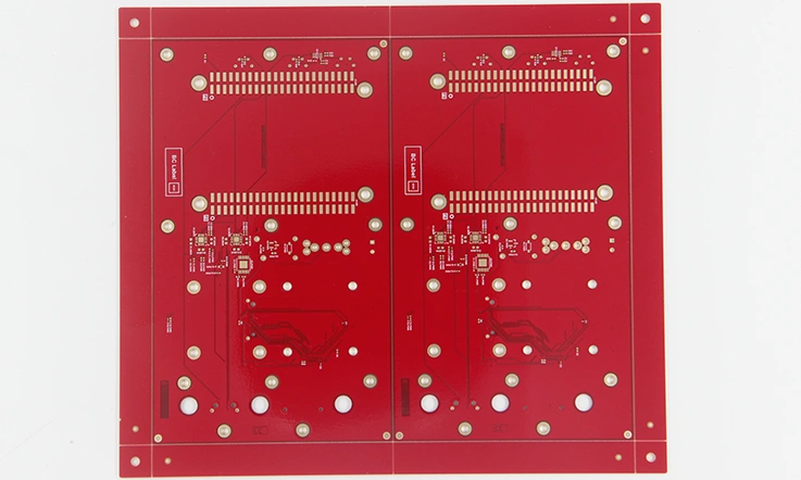
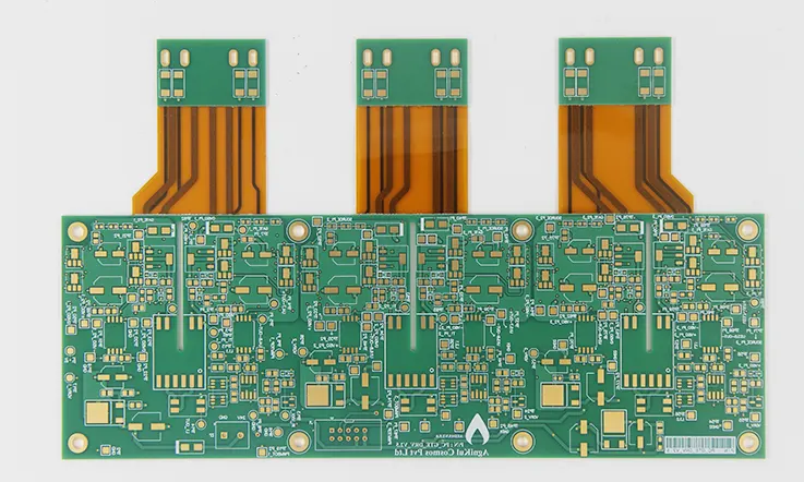
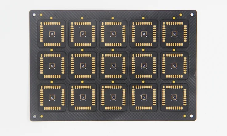
High-Density Interconnect (HDI) Multilayer PCB is a technology that enables high-performance circuit designs with increased density and superior signal integrity. From smartphones to military applications, HDI technology is becoming the foundation for smaller, more efficient electronic devices.
Compared to traditional multilayer PCBs, HDI PCBs incorporate complex via structures, fine-pitch traces, and advanced lamination techniques. Understanding the manufacturing processes, material choices, and the benefits of HDI PCBs is essential for anyone involved in designing or producing cutting-edge electronics.
What is HDI Multilayer PCB and Why is it Important?
HDI Multilayer PCB (High-Density Interconnect) uses microvias (blind, buried, stacked) and fine-pitch traces to maximize circuit density while maintaining excellent electrical performance.
1. Key Advantages of HDI Multilayer PCB-
| Feature | HDI Multilayer PCB | Standard Multilayer PCB |
| Circuit Density | Higher, supports finer traces | Limited by mechanical drilling |
| Signal Integrity | Superior, reduces crosstalk | Affected by trace length |
| Size & Weight | More compact, lightweight | Bulkier design |
| Thermal Management | Optimized for high-speed applications | Limited dissipation capacity |
| Cost Considerations | Higher initial cost, but better ROI | Lower cost, less performance |
HDI PCBs help devices achieve higher performance and reduced size, providing clear advantages in industries like 5G, aerospace, and high-speed computing.
Core Features of HDI Multilayer PCB
HDI PCBs bring a range of advanced design and manufacturing techniques that allow for the development of high-density, high-performance circuit boards.
1. Microvia Technology: Blind, Buried, and Stacked Vias-
Microvias are a main feature of HDI PCBs. Unlike traditional through-hole vias, microvias are much smaller and allow for denser interconnections and efficient routing.
| Microvia Type | Description | Applications |
| Blind Via | Connects outer layers to inner layers but doesn’t go through the PCB | High-density BGA components |
| Buried Via | Connects internal layers, improving layout flexibility | Multi-layer signal routing |
| Stacked Via | Multiple microvias stacked for high-density connections | High-speed, high-frequency applications |
These microvia technologies enable more reliable electrical connections and ensure that high-frequency signals can be transmitted with less loss.
2. Sequential Lamination & Layer Stack-up Strategies-
Sequential lamination allows for the creation of multi-layer interconnections that offer optimal signal transmission.
●3+N+3 Stack-up: Used for high-speed applications
●2+4+2 Stack-up: Common in high-performance networking devices
Proper stack-up ensures signal reliability and thermal efficiency, preventing issues like signal reflection and EMI interference.
3. Signal Integrity and Impedance Control in HDI PCB Design-
Signal integrity affects high-density designs, and impedance control keeps signals steady as they move through the PCB.
●Trace width and spacing calculations: Ensure signals travel without interference.
●Differential pair routing: Common in USB 3.0, PCIe, and RF applications.
●Power integrity considerations: Maintain stable voltage across all layers.
Maintaining signal integrity is especially important when handling high-speed data transfer, as poor routing can lead to unreliable signal transmission.
HDI PCB vs. Standard Multilayer PCB – Key Differences
When comparing HDI to standard PCBs, the differences become clear in terms of manufacturing techniques, material choices, and performance capabilities.
1. Manufacturing Process Differences-
HDI PCBs use laser-drilled microvias, high-resolution imaging, and advanced plating methods, while traditional PCBs rely on mechanical drilling and simpler vias.
| Manufacturing Process | HDI PCB | Standard PCB |
| Drilling Method | Laser drilling | Mechanical drilling |
| Trace Width | As low as 50μm | Typically above 100μm |
| Layer-to-Layer Interconnects | Microvias & stacked vias | Through-hole vias |
HDI’s advanced manufacturing processes enable better electrical performance and higher layer density in compact designs.
2. Material Selection and Reliability Considerations-
HDI PCBs are often made with high-Tg materials, low-Dk substrates, and high-frequency FR-4, ensuring optimal signal transmission and reliability even in high-performance environments.
●Low-Dk materials reduce signal delay and increase high-frequency capabilities.
●High-Tg substrates ensure greater thermal stability.
●Advanced prepreg materials improve layer bonding and electrical insulation.
3. Cost Implications and Production Challenges-
HDI PCBs involve higher initial costs due to the advanced processes, but these costs are outweighed by their performance in demanding applications.
●Smaller size and reduced weight lead to lower assembly costs over time.
●Enhanced signal quality reduces the need for additional layers or complex designs.
●Increased durability minimizes the need for repairs or revisions.
For businesses focused on cutting-edge technology, adopting HDI PCB is a smart investment that provides better performance and reliability in the long run.
HDI Multilayer PCB Stack-Up and Material Selection
Designing an HDI Multilayer PCB requires a methodical approach to material selection and layer configuration to support high-density routing, controlled impedance, and thermal stability. With increasing demand for high-frequency, high-speed, and miniaturized electronic systems, we must evaluate dielectric properties, thermal expansion characteristics, and signal integrity considerations when choosing laminates and defining the stack-up.
Choosing the Right Laminate for HDI Multilayer PCB
Selecting a laminate for HDI Multilayer PCB fabrication is not solely about mechanical durability—it directly influences signal propagation, thermal performance, and manufacturability. The choice depends on dielectric constant (Dk), dissipation factor (Df), coefficient of thermal expansion (CTE), and thermal conductivity (k-value).
Material Considerations for HDI PCB Laminates:
●Dielectric Constant (Dk): Lower values reduce signal delay and allow faster signal transmission, improving performance in high-speed applications.
●Dissipation Factor (Df): Lower Df materials reduce signal attenuation and ensure better signal integrity over long traces.
●Coefficient of Thermal Expansion (CTE): A lower CTE minimizes stress on microvias and interconnections under thermal cycling.
●Thermal Conductivity (k-value): Higher thermal conductivity materials enhance heat dissipation in power-dense designs.
Common HDI PCB Substrates and Their Properties-
| Laminate Type | Dielectric Constant (Dk @ 1GHz) | Dissipation Factor (Df) | CTE (ppm/°C) | Thermal Conductivity (W/m·K) | Typical Applications |
| FR-4 High-Tg | 4.2 – 4.5 | 0.015 | ~180 | 0.25 | General-purpose multilayer PCBs |
| Polyimide | 3.5 – 4.0 | 0.004 | ~55 | 0.3 | Aerospace, military, flexible circuits |
| Rogers 4000 Series | 3.38 – 3.55 | 0.002 | ~50 | 0.6 | RF, microwave, and millimeter-wave PCBs |
| Ceramic-Filled PTFE | 2.2 – 2.6 | 0.001 | ~30 | 0.7 | 5G, satellite, radar systems |
For high-frequency RF and microwave HDI PCBs, ceramic-filled PTFE laminates or Rogers 4000 series materials offer superior signal integrity with minimal dielectric loss.
Advanced HDI PCB Stack-Up Configurations
The stack-up of an HDI PCB determines layer distribution, power integrity, and impedance control. We must optimize signal routing, ensure proper return paths, and select via structures that enhance reliability and manufacturability.
Common HDI PCB Stack-Up Structures-
| Stack-Up Type | Layer Count | Via Structure | Application |
| 1+N+1 | 4–6 layers | Single-layer microvias | Consumer electronics, handheld devices |
| 2+N+2 | 6–10 layers | Stacked and staggered microvias | 5G infrastructure, automotive radar |
| Any-Layer HDI | 10+ layers | Laser-drilled vias on all layers | Aerospace, high-speed computing |
Considerations for HDI PCB Layer Stack-Up:
●Microvia Placement: Staggered microvias reduce mechanical stress compared to stacked microvias, improving reliability.
●Power and Ground Planes: Dedicated power layers enhance power distribution network (PDN) performance and reduce noise.
●Dielectric Layer Thickness: Thin dielectric layers improve high-speed signal transmission but require precise impedance control.
For high-speed applications, our designers often use a 2+N+2 stack-up, balancing signal integrity and manufacturability, while Any-Layer HDI configurations allow complete design freedom with microvias interconnecting all layers, albeit at a higher production cost.
How HDI Multilayer PCB Improves Reliability with Advanced Materials?
Material reliability in HDI PCBs extends beyond mechanical durability—low-loss dielectric materials, embedded EMI shielding, and thermally conductive substrates contribute to long-term stability in demanding environments.
Key Material Properties Affecting HDI PCB Reliability-
| Material Property | Impact on HDI PCB Performance |
| Low-Loss Dielectric | Maintains signal integrity by minimizing transmission loss |
| High Tg (Glass Transition Temperature) | Reduces risk of warpage and delamination under thermal stress |
| Embedded EMI Shielding | Improves electromagnetic compatibility (EMC) by suppressing interference |
| Low CTE Substrates | Reduces microvia fatigue and ensures longevity under thermal cycling |
For high-reliability applications such as aerospace and satellite electronics, selecting a high-Tg, low-CTE material prevents mechanical failures caused by thermal expansion mismatches. Embedded EMI shielding layers further mitigate signal degradation in high-frequency circuits.
Advanced HDI Multilayer PCB Design and Engineering Optimization
Designing HDI (High-Density Interconnect) Multilayer PCBs calls for a solid grasp of advanced manufacturing methods and engineering strategies. As electronic devices push for higher performance, compact layouts, and more intricate circuitry, fine-tuning the design and material selection of HDI PCBs becomes a top priority.
Successful HDI PCB design combines aspects such as layer stack-up optimization, via technology, power integrity, and thermal management. Through careful selection of materials and design strategies, we can create high-performance, reliable, and cost-effective HDI PCBs that meet the rigorous demands of industries like telecommunications, automotive, aerospace, and consumer electronics.
Optimizing Layer Stack-up for HDI Multilayer PCB Performance
The layer stack-up configuration directly affects signal behavior, power distribution, and overall circuit board efficiency in HDI Multilayer PCB design. Optimizing this structure involves careful selection of materials, impedance control, and thermal management to maintain stable performance in high-density applications.
1. Choosing High-Frequency PCB Materials-
The choice of materials plays a huge role in how well an HDI PCB performs. High-frequency materials, such as PTFE, Rogers, or Arlon laminates, are commonly selected for designs requiring low signal loss and high-frequency operation.
These materials help in maintaining signal clarity across high-speed applications by minimizing dielectric loss. Therefore, we must balance cost, reliability, and performance when choosing materials for HDI boards, especially in 5G communication systems and military radar applications.
2. Copper Trace Thickness and Controlled Impedance Routing-
Copper trace thickness and controlled impedance routing directly impact signal quality and timing accuracy in HDI PCBs. Selecting the appropriate trace thickness ensures proper impedance matching, commonly set at 50Ω for single-ended traces and 100Ω for differential pairs, to maintain stable signal transmission.
| Design Factor | Effect on HDI PCB Performance |
| Trace Thickness | Influences impedance control and current handling capacity |
| Impedance Routing | Ensures signal fidelity and minimizes reflection |
Impedance mismatches can lead to signal reflection, loss, and distortion, especially in high-frequency data transmission. Carefully designing the impedance path can ensure optimal signal transmission without interference.
Effects of Dielectric Constant on HDI PCB Signal Transmission-
The dielectric constant (Dk) of PCB materials affects signal speed and capacitance between traces. In HDI designs, lower Dk materials are often preferred to achieve faster signal transmission and reduce signal degradation.
When selecting materials, considering the relationship between Dk and frequency helps minimize signal loss and maintain consistent performance. For high-speed circuits, using low-Dk materials supports signal stability at higher frequencies.
Via Technology in HDI Multilayer PCB Design
HDI PCBs utilize advanced via technologies to support high-density routing and compact layouts. Vias create electrical connections between layers, and selecting the right type directly affects performance and long-term reliability.
1. Stacked vs. Staggered Microvias – Which is Better?
In HDI PCBs, microvias are used for routing connections between layers. The two main types are stacked microvias (vias that are drilled through multiple layers) and staggered microvias (vias that are placed between layers).
●Stacked Microvias: Offer higher density and smaller footprint but are more complex to manufacture.
●Staggered Microvias: Easier to manufacture but may require more layers for routing.
The choice between stacked and staggered microvias depends on the specific design requirements, including circuit density, layer count, and cost constraints.
2. Via-in-Pad Technology for High-Density Designs-
Via-in-pad technology places vias directly in the pads where components are mounted, allowing for dense and efficient routing in HDI PCBs. This technology is commonly used in high-density interconnect designs, enabling better routing and more compact layouts.
| Technology | Benefits | Challenges |
| Via-in-Pad | Improved density, better routing | Increased manufacturing complexity, higher cost |
However, via-in-pad technology can increase the cost and complexity of manufacturing, as it requires more advanced processes like laser drilling and via plating. The trade-off between density and production cost needs to be evaluated carefully during the design phase.
3. Minimizing Electromagnetic Interference (EMI) in HDI PCBs-
Electromagnetic interference (EMI) is a major concern in HDI PCB design, especially in high-speed circuits and signal integrity-sensitive applications. Using techniques like shielding, ground planes, and proper via placement helps minimize EMI and ensure that signals remain clean and distortion-free.
| EMI Mitigation Technique | Effect on HDI PCB Performance |
| Ground Planes | Provides continuous return paths for signals, reducing noise. |
| Shielding | Helps block external noise from affecting signal quality. |
| Via Placement | Proper placement helps reduce crosstalk and signal degradation. |
Designing HDI PCBs with EMI control in mind helps maintain stable operation in environments where signal precision is non-negotiable, such as aerospace and medical applications.
Power Integrity and Thermal Management in HDI Multilayer PCB
Power integrity and thermal management are major considerations when designing high-performance HDI PCBs. Proper attention to power distribution and heat dissipation can help improve the overall reliability and performance of the PCB.
1. Thermal Via Arrays for Efficient Heat Dissipation-
Thermal via arrays are designed to help direct heat from the components to heat sinks or other layers for dissipation. These arrays provide efficient thermal management and prevent overheating of sensitive components.
| Thermal Management Method | Effect on HDI PCB Performance |
| Thermal Via Arrays | Helps direct heat away from components, improving reliability. |
| Heat Sinks | Dissipates heat more effectively in high-power applications. |
By optimizing thermal via arrays, we can ensure that HDI PCBs perform under high-heat conditions without sacrificing signal integrity.
2. Power Distribution Network (PDN) Design in HDI PCBs-
A Power Distribution Network (PDN) ensures that consistent voltage is delivered to each part of the circuit. In HDI PCBs, the PDN design must account for layer count, component placement, and signal trace routing to prevent voltage drops and power integrity issues.
A well-designed PDN helps ensure that high-speed digital signals are unaffected by voltage fluctuations and that components receive stable power.
3. Decoupling Capacitors and Power Stability Considerations-
Decoupling capacitors are used in HDI PCBs to stabilize voltage levels and filter out noise from the power supply. Proper placement of decoupling capacitors near components helps ensure that high-speed signals are not disrupted by power fluctuations or electrical noise.
HDI Multilayer PCB Manufacturing Process & Quality Control
Producing HDI Multilayer PCBs requires advanced engineering, precise fabrication techniques, and thorough quality checks. These boards are widely used in high-performance electronics, including military radar systems, aerospace applications, and high-speed communication devices.
With increasing demands for miniaturization and enhanced signal performance, every stage of the manufacturing and assembly process must be fine-tuned to ensure consistency and reliability. From microvia drilling and copper plating to surface finishing and stress testing, a well-executed production process leads to superior results.
Advanced Fabrication Techniques for HDI Multilayer PCB
The fabrication of HDI Multilayer PCBs follows a sequence of specialized steps designed to support high-density interconnects and complex layer configurations. Each step plays a role in shaping the durability, conductivity, and signal transmission capabilities of the finished product.
1. Sequential Build-Up (SBU) Manufacturing Process-
The SBU method is widely used in HDI PCB production, allowing for the gradual addition of layers and the formation of precisely structured microvias. Unlike conventional multilayer PCBs, which rely on a single lamination process, HDI boards are built in stages to accommodate higher circuit density and improved electrical performance.
This structured construction process allows for more efficient routing, making it well-suited for applications that demand both compact layouts and high functionality.
2. Laser Drilling vs. Mechanical Drilling for Microvias-
Microvia formation is a core step in HDI PCB fabrication, as it enables electrical connections between tightly packed layers. The choice of drilling technique depends on the design complexity and performance requirements.
●Laser drilling is commonly used for blind and buried vias, as it allows for the creation of precise, small-diameter holes without causing damage to adjacent layers.
●Mechanical drilling is suitable for larger vias but becomes less effective when working with fine-pitch designs and dense interconnections.
As electronic devices become more compact, laser drilling remains the preferred choice due to its ability to accommodate high-density layouts without compromising structural integrity.
3. Copper Plating and High-Density Interconnect Traces-
To establish strong electrical connections between layers, copper plating is applied to the drilled microvias and circuit traces. Several techniques are used to enhance conductivity and durability:
●Electroless copper deposition provides an initial layer of conductive material in microvias.
●Electroplating builds up copper thickness to support signal transmission and mechanical strength.
●Advanced etching techniques allow for fine-line routing, helping preserve signal integrity in high-frequency applications.
These steps contribute to the overall performance and longevity of the PCB, reducing the likelihood of electrical failure due to poor interconnect reliability.
Surface Finishing and SMT Assembly for HDI Multilayer PCB
Once the PCB is fabricated, the next steps involve surface finishing and component assembly. These processes ensure that the board is prepared for efficient soldering and long-term protection against oxidation.
1. Choosing the Right Surface Finish-
Different surface finishes provide varying levels of solderability, corrosion resistance, and compatibility with fine-pitch components.
●ENIG (Electroless Nickel Immersion Gold) offers a flat surface, making it suitable for BGA and fine-pitch components.
●HASL (Hot Air Solder Leveling) is a widely used finish that provides cost-effective protection for standard applications.
●OSP (Organic Solderability Preservative) is an eco-friendly option, often chosen for high-speed signal transmission applications.
Selecting the appropriate finish depends on factors such as operating environment, assembly requirements, and long-term performance expectations.
2. Fine-Pitch Component Placement and SMT Challenges-
As component sizes continue to shrink, Surface Mount Technology (SMT) has become the preferred assembly method for HDI PCBs. However, high-density designs present unique challenges during soldering and component placement:
●Solder bridging can occur when closely spaced pads cause unintended electrical connections.
●Tombstoning happens when uneven heating lifts small passive components during reflow soldering.
●X-ray inspection is often required to detect hidden solder joint defects, especially in BGAs and chip-scale packages (CSPs).
Managing these challenges ensures that the assembled board meets electrical and mechanical expectations, reducing the risk of post-production failures.
3. Lead-Free Manufacturing and RoHS Compliance-
With increasing regulations surrounding eco-friendly manufacturing, HDI PCB production follows RoHS (Restriction of Hazardous Substances) guidelines. These regulations mandate:
●The elimination of lead, mercury, and other hazardous materials from PCB finishes.
●The use of halogen-free laminates to reduce environmental impact.
●Adjustments to reflow soldering processes due to higher melting points in lead-free solders.
Ensuring compliance with global environmental standards makes HDI PCBs suitable for medical, automotive, and industrial applications where sustainability is a consideration.
Reliability Testing & Quality Assurance for HDI Multilayer PCB
Once assembled, HDI PCBs must undergo thorough testing and validation to confirm that they meet performance and durability requirements.
1. Electrical Performance Testing and Impedance Validation-
To maintain consistent signal transmission, HDI PCBs go through a series of electrical tests:
●Time-Domain Reflectometry (TDR) checks for impedance variations and signal reflections.
●Flying probe testing verifies continuity, shorts, and open circuits in the PCB traces.
●High-speed signal analysis ensures compliance with 5G, RF, and other high-frequency applications.
These evaluations help prevent signal degradation and connectivity issues, particularly in data-driven and wireless communication devices.
2. Automated Optical Inspection (AOI) and X-ray Inspection-
With high-density circuit layouts, traditional inspection methods are often insufficient. Advanced technologies such as AOI and X-ray analysis are used to detect:
●Micro-cracks in solder joints, which can compromise electrical connections.
●Misaligned components, which may affect circuit performance.
●Hidden defects within internal layers, which are difficult to identify through standard visual inspection.
Implementing these inspection techniques minimizes the chances of defects reaching the final product stage.
3. Environmental Stress Testing for Military-Grade HDI PCBs-
For defense and aerospace applications, HDI PCBs must withstand extreme conditions. Environmental stress testing includes:
●Thermal cycling, which simulates exposure to temperature fluctuations and assesses material expansion/contraction effects.
●Vibration and shock testing, which evaluates resistance to mechanical stress and high-G-force conditions.
●Humidity and corrosion resistance testing, which ensures long-term durability in harsh environments.
Overcoming Challenges in HDI Multilayer PCB Manufacturing
Bringing HDI Multilayer PCBs from concept to production isn’t a straightforward task. As designs become more compact and electronic devices demand higher performance, we must navigate multiple obstacles, from signal interference and thermal issues to cost-performance balance.
Addressing these challenges requires a well-thought-out approach to PCB design, material selection, and manufacturing processes. The sections below break down specific areas that require attention to achieve high-density interconnect reliability and efficiency.
Signal Integrity and Crosstalk Management in HDI PCB Layouts
Ensuring clear, distortion-free signals is a top priority in HDI Multilayer PCB design. Without proper layout strategies, signals can degrade due to interference, reflections, and unintended electromagnetic interactions.
1. High-Speed PCB Routing Strategies-
When designing HDI PCBs, optimizing routing paths reduces signal loss and transmission delays. we apply several techniques to keep signals clean:
●Length matching for differential pairs ensures that signals reach their destination simultaneously.
●Minimized via transitions reduce disruptions in transmission paths.
●Layer-to-layer impedance control helps maintain consistent signal characteristics.
Careful routing prevents distorted waveforms and data errors in high-frequency applications.
2. Minimizing Parasitic Capacitance and Inductance-
Unintended capacitance and inductance can lead to delays, unwanted voltage fluctuations, and unpredictable circuit behavior. Techniques to limit these effects include:
●Maintaining uniform trace widths and spacing to reduce stray capacitance.
●Avoiding sharp-angle bends, which can introduce resistance and affect signal flow.
●Placing ground planes close to signal layers to stabilize return paths.
Fine-tuning the layout prevents unexpected interference and maintains signal consistency.
3. Via Optimization to Reduce Crosstalk and Signal Reflections-
Vias serve as essential interconnects in HDI PCBs, but improper placement can lead to crosstalk, signal loss, and unwanted reflections. Best practices for via design include:
●Using back-drilled vias to eliminate unused stubs.
●Spacing vias apart to limit coupling between signals.
●Choosing between stacked and staggered vias based on density and performance needs.
Proper via placement keeps signals clear and interference-free in high-speed designs.
Avoiding Thermal Expansion and Warpage in HDI Multilayer PCB
As circuit density increases, so do thermal challenges. Differences in material expansion rates can lead to board deformation, solder joint stress, and electrical failures over time.
1. Material Selection for Thermal Stability-
Choosing materials that handle temperature shifts and repeated heating cycles ensures a stable and long-lasting PCB structure. We evaluate materials based on:
●CTE (Coefficient of Thermal Expansion)—matching materials with similar expansion rates reduces stress.
●Tg (Glass Transition Temperature)—substrates with higher Tg withstand soldering heat without deformation.
●Copper-invar-copper (CIC) laminates—reinforce boards against warping in high-temperature environments.
Matching materials to operating conditions prevents cracking, delamination, and mechanical strain.
2. Manufacturing Techniques to Minimize PCB Warpage-
Thermal warping can affect assembly and functionality. Production techniques that help keep boards flat include:
●Balanced copper distribution across layers to reduce uneven shrinkage.
●Slow, controlled cooling cycles after lamination to prevent stress buildup.
●Proper support during reflow soldering to maintain shape stability.
Consistent manufacturing processes help maintain PCB reliability in changing thermal environments.
3. Testing Methodologies for Long-Term Reliability-
Before deployment, HDI Multilayer PCBs undergo testing to ensure they withstand mechanical and thermal stress. Common testing methods include:
●Thermal cycling tests to simulate long-term heating and cooling exposure.
●Solder fatigue analysis to check for cracks or weak points in joints.
●Environmental chamber testing to expose boards to real-world conditions like humidity and extreme temperatures.
Thorough testing helps manufacturers deliver durable, high-performance HDI PCBs across industries.
Cost vs. Performance Trade-offs in HDI Multilayer PCB
Balancing manufacturing expenses with performance goals is a constant challenge. While HDI PCBs offer enhanced functionality, adding extra layers and features can significantly increase production costs.
1. Cost-Effective Material Selection for HDI PCBs-
Not every design requires high-performance laminates. Choosing materials that match the application can reduce unnecessary expenses. Options include:
●Standard FR4 laminates for consumer electronics with moderate performance needs.
●Enhanced epoxy and polyimide for applications requiring better heat and chemical resistance.
●PTFE-based substrates for RF and high-frequency applications where signal integrity is a top concern.
Selecting the right material ensures that costs remain controlled without sacrificing PCB performance.
2. Optimizing PCB Panelization for Reduced Waste-
Production efficiency plays a big role in keeping costs manageable. Panelization strategies help maximize yield while minimizing material loss:
●Adjusting PCB layout orientation to fit more units per panel.
●Reducing unnecessary routing gaps to minimize unused material.
●Using V-grooves and breakaway tabs for easier depanelization.
A well-planned panelization setup ensures cost-effective manufacturing without excess waste.
3. Balancing Advanced Features with Manufacturing Efficiency-
Adding microvias, thinner traces, and additional layers increases complexity and costs. Engineers weigh performance needs against fabrication constraints by:
●Assessing whether additional layers are truly necessary for the design.
●Using simplified via structures where possible to lower drilling costs.
●Aligning designs with standard manufacturing capabilities to avoid custom fabrication fees.
By streamlining PCB complexity, production remains efficient while delivering high-density interconnect benefits.
Emerging Technologies in HDI Multilayer PCB
As electronic devices continue to push the limits of performance, miniaturization, and integration, HDI Multilayer PCBs have become an indispensable part of modern design. From semiconductor packaging advancements to high-frequency applications, HDI PCB technology is evolving rapidly to meet industry demands. The following sections delve into cutting-edge developments and their impact on PCB engineering.
Semiconductor Packaging and HDI PCB Integration
Modern semiconductor packaging methods demand PCBs with higher density, enhanced signal transmission efficiency, and robust thermal management. HDI Multilayer PCBs, featuring microvia structures and ultra-thin dielectric layers, are integral to advanced packaging techniques such as Fan-Out Wafer-Level Packaging (FOWLP) and System-in-Package (SiP).
Comparison of Semiconductor Packaging Types and HDI PCB Interconnect Requirements
| Packaging Type | Interconnect Requirements | Applications |
| Fan-Out Wafer-Level Packaging (FOWLP) | High-density routing, microvia interconnects | AI computing, 5G, mobile devices |
| Chip-On-Board (COB) | Direct chip bonding, minimal signal path | Sensors, medical electronics |
| System-in-Package (SiP) | Multi-chip integration, enhanced thermal conductivity | Wearable devices, IoT applications |
| Flip-Chip | BGA pads, fine-pitch routing | Servers, GPUs |
As processing speeds increase, optimizing HDI PCB structures for semiconductor integration ensures stable signal integrity and minimal power loss. Engineers must consider factors like via-in-pad technology and low-loss dielectric materials when designing for next-generation packaging solutions.
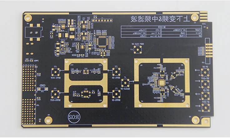
RF and Microwave HDI Multilayer PCB Design Considerations
With the rise of 5G, millimeter-wave radar, and satellite communications, RF and microwave PCB circuit designs are placing new demands on PCB technology. HDI PCBs designed for RF applications require precise impedance control, minimal signal attenuation, and materials capable of maintaining stable dielectric properties across varying frequencies.
Material Comparison for RF and Microwave HDI PCB Applications-
| Frequency Range | Recommended PCB Material | Dielectric Constant (Dk) | Loss Factor (Df) |
| <1GHz | FR-4 | 4.2 | 0.02 |
| 1-10GHz | Rogers 4350B | 3.48 | 0.0037 |
| 10-30GHz | Isola Astra MT77 | 3.00 | 0.0017 |
| >30GHz | Taconic TLY-5 | 2.20 | 0.0009 |
To reduce signal degradation, we implement advanced routing strategies such as controlled impedance transmission lines and differential pair routing. High-frequency applications also benefit from HDI PCB features like low-inductance ground planes and minimal via stubs to prevent signal reflections.
Innovations in HDI Multilayer PCB Surface Finishing
Surface finish plays a decisive role in HDI PCB manufacturing, influencing solderability, oxidation resistance, and long-term reliability. The choice of surface finish impacts assembly processes, electrical performance, and compatibility with high-frequency signals.
Comparison of Surface Finishing Techniques for HDI PCBs-
| Surface Finish | Flatness | Solderability | Common Applications | Cost |
| ENIG (Electroless Nickel Immersion Gold) | High | Excellent | High-speed circuits, telecom equipment | Medium |
| ENEPIG (Electroless Nickel Electroless Palladium Immersion Gold) | High | Superior | Advanced semiconductor packaging | High |
| HASL (Hot Air Solder Leveling) | Low | Good | Traditional PCB, low-cost applications | Low |
| OSP (Organic Solderability Preservative) | Medium | Moderate | Consumer electronics, short-lifespan devices | Low |
For HDI PCBs used in high-reliability applications, ENEPIG provides superior wire bonding capabilities and long-term oxidation resistance, making it suitable for micro-pitch components. Conversely, ENIG offers excellent flatness and conductivity for high-speed circuits but may require careful process control to prevent black pad defects.
HDI Multilayer PCB – FAQs
1.Why use stacked microvias in HDI PCBs?
They enable higher routing density, better signal transmission, and compact multi-layer interconnections for high-speed applications.
2.How do HDI PCBs enhance signal integrity?
Optimized trace routing, controlled impedance, and microvias minimize signal loss, EMI, and crosstalk, improving high-frequency performance.
3.What are the challenges of ultra-thin HDI PCBs?
Preventing warpage, precise lamination, fine-line etching, and thermal expansion control are key manufacturing concerns.
4.How do dielectric materials impact HDI PCBs?
Materials like Rogers or PTFE reduce signal loss, while FR4 is a cost-effective option for moderate performance.
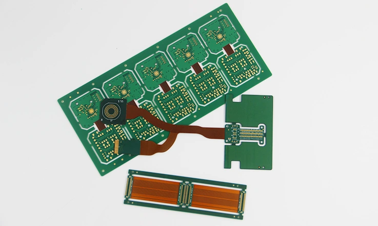
5.Can HDI technology be used in flexible PCBs?
Yes, HDI enhances connectivity in rigid-flex and flexible circuits for compact, high-performance applications.
6.What are common HDI PCB layer counts?
Typically 4 to 16 layers, with advanced designs exceeding 20 layers for complex applications.
7.How does sequential lamination improve reliability?
It enhances layer stacking precision, reduces stress on interconnects, and strengthens mechanical durability.
8.Which surface finishes are best for HDI assembly?
ENEPIG and ENIG offer smooth surfaces and strong solderability, while OSP is a budget-friendly option.
9.How does HDI PCB support miniaturization in medical devices?
High-density routing and microvias enable smaller, high-performance designs for implantable and portable electronics.


