
The 3+N+3 HDI PCB circuit board stands as a groundbreaking advancement in the arena of printed circuit board design and production. With its ability to achieve greater routing density and improved signal integrity has affirmed its integral role in the fabrication of compact, high efficiency electronic equipment.
This post seeks to probe into the notable characteristics, advantages, design, and production of the 3+N+3 HDI PCB, elucidating its important in contemporary electronic products.
What is 3+N+3 HDI PCB Circuit Board?
3+N+3 High-Density Interconnect Printed Circuit Board refers to a specific type of PCB design that incorporates multiple layers and advanced interconnect technologies to achieve high-density routing and improved performance. Let’s break down the components of the term:
● 3: The digit “3” symbolises the core layers of the PCB. These are the inner layers that provide structural integrity and typically consist of copper traces and insulating substrate material.
● N: The alphabet “N” denotes the tally of intermediary layers in the PCB stack up. These layers are inducted amidst the core layers to augment the routing compactness and introduce supplementary functionality. The legit count of intermediary strata might fluctuate based on the exact design prerequisites.
● 3: Analogous to the inaugural “3,” this figure signifies the outer layers of the PCB. These layers are positioned at the peak and base of the stack up, provide additional space for routing.
The combination of core layers, intermediary layers, and outer layers facilitate a high density interconnect structure, granting permission for intricate and condensed circuit design. This type of PCB is commonly used in applications where space is limited, and the need for miniaturization and high-speed performance is critical.
HDI PCB often employ advanced technologies such as microvias, blind vias, and buried vias to achieve the desired routing density. These technologies allow for smaller via sizes, tighter trace widths and spacing, and increased layer count, resulting in improved signal integrity and reduced signal propagation delays.
On the whole, 3+N+3 HDI PCB provide a pathway to accomplish high density circuit layouts with amplified performance traits, rendering them appropriate for utilization in applications including smartphones, tablets, medical apparatus and high speed communication infrastructures.
So What is 3+N+3 HDI PCB Stack-up Mean?
Printed Circuit Board stack up refers to the arrangement of different layers of materials that make up a PCB. HDI PCB are a type of PCB design that allows for higher component density and miniaturization. 3+N+3 HDI PCB stack up is a specific configuration that offers enhanced performance and increased complexity for advanced electronic designs.
The “3+N+3” denotation in the stack up corresponds to the count of core layers, signal layers and routing layers in the PCB. The “N” represents the number of signal layers, which can vary based on the specific design requirements. Core layers typically comprised of FR-4, a commonly used PCB substrate material, while signal and routing layers can employ thinner and more advanced materials such as high-speed laminates or flexible materials.
In a 3+N+3 HDI PCB stack up arrangement the core layers are surrounded by signal layers, on both sides. These signal layers are then enclosed by a routing layer. The stacking configuration is symmetrical to maintain impedance and signal integrity throughout the board.
The 3+N+3 stack up offer additional flexibility in routing and interconnect options, allowing for complex designs with multiple signal layers and improved signal integrity. It offers better control over impedance matching, reduces noise and enables high speed data transmission.
3+N+3 HDI PCB Stack up
The 3+N+3 HDI High-Density Interconnect stacking configuration provides diverse via layouts, including staggered vias, blind vias, stacked vias and cross layer blind vias. Of these options, the staggered vias stack-up design is often favored owing to its cost-efficiency. A multitude of engineers select the 3+N+3 stack up with staggered vias to curtail fabrication expenses.
Nonetheless, the cross layer blind via design, despite being more intricate, provides superior performance,, thereby making it befitting for advanced technological products. This design typically precipitates in loftier manufacturing prices in comparison to other 3+N+3 stack up configurations.
3+N+3 HDI PCB with staggered vias
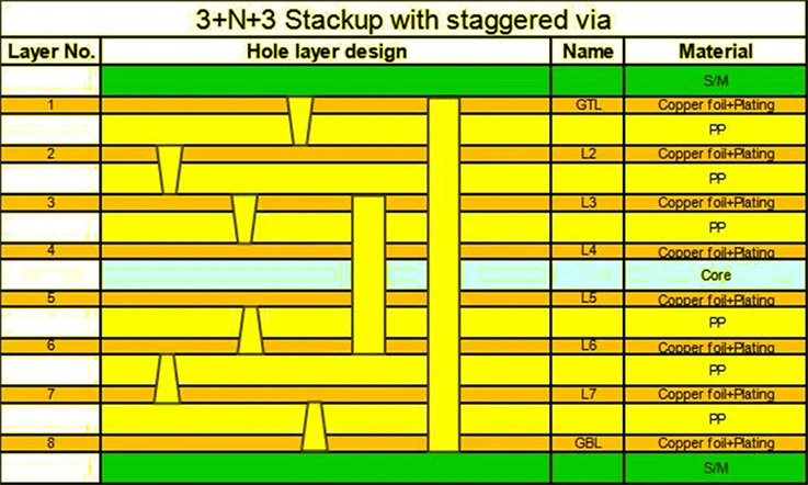
The 3+N+3 HDI stack up incorporating staggered vias exhibits similarities with the 2+N+2 HDI configuration, differing primarily in the lamination times required for layer integration. In the case of Type III PCB stack up, the connection between consecutive adjacent layers necessitates the utilization of wire bonding techniques.
Presented here is an 8-layer 3+N+3 HDI PCB with Staggered vias Stack up. It bears resemblance to the Type III HDI stack up, allowing reference to the 2-type stack up for further understanding. The current Type III HDI stack up entails the embedding of vias within the inner multi-layer board, requiring four pressing cycles for completion. This is primarily due to the absence of stacked hole design in the HDI stack up, resulting in normal production challenges. However, by optimizing the buried hole arrangement to encompass L2-L7 instead of L3-L6, one pressing cycle can be eliminated, enabling process optimization and cost reduction.
3+N+3 HDI PCB with stacked vias
The advocated stack up design involves a 3+n+3 HDI layout integrating stacked vias. The manufacturing progression comprises an initiating boring phase to establish the L3-L6 buried vias, succeeded by subsequent drilling of the L3-L4 and L5-L6 buried vias. Moreover, the L1-L2 blind vias get purposefully stacked on top the L3 buried vias. The concluding act involves boring the through vias to culminate the stack up. For pictorial elucidation and additional specifics, kindly consult the furnished Type III HDI stack up diagram.
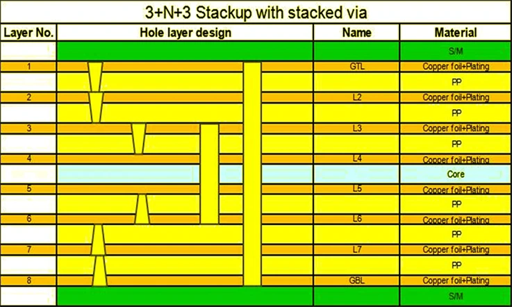
The structure of the discussed board follows a (1+1+1+N+1+1+1) arrangement, representing a challenging 3+N+3 configuration that currently poses manufacturing difficulties in the industry. The inner multi-layer board incorporates buried holes, specifically located in the L3-L6 region, requiring four lamination cycles for completion. The primary challenge arises from the presence of cross-layer blind hole designs, which demand specialized manufacturing capabilities.
HDI PCB fabricators deficient in the requisite technical acumen might grapple with challenges while generating such secondary laminate components. To surmount this, a refinement tactic entails transposing the cross layer blind holes from L1-L3 to L1-L2 and L2-L3, effectively splitting the blind holes. This staggered blind hole bifurcation methodology affords substantial merits, inclusive of diminishing production expenditures and optimized manufacturing processes.
3+N+3 HDI PCB: Benefits
3+N+3 HDI PCB offer advantages when compared to conventional PCB. Lets delve into some of these benefits:
Increased Design Flexibility:
Employing HDI technology paves the road for greater routing density and the possibility for miniaturizing electronic devices. With the 3+N+3 stack up, which typically consists of three signal layers and multiple stacked microvia layers, designers can achieve complex and compact circuit layouts. This enables more functionality in smaller form factors, making it ideal for applications where space is limited.
Improved Signal Integrity:
The use of microvias in HDI PCB helps to reduce the length of signal traces and minimize parasitic capacitance and inductance. This leads to improved signal integrity, reduced signal loss, and better impedance control. HDI technology allows for controlled impedance routing, enabling high-speed signal transmission with minimal signal degradation.
Enhanced Power and Ground Distribution:
HDI PCB excel in power and ground distribution thanks to the incorporation of extra internal power and ground planes. The stacked layers of microvias afford an effective power conveyance strategy and enhance the consistency of the ground plane. This results in a noticeable reduction in power related noise, significant elevation in the quality of signal transmission, and a pronounced enhancement in overall device performance.
Increased Design Density:
The higher routing density achieved with HDI PCBs allows for more components to be placed on the board, enabling advanced functionalities and increased design complexity. The use of microvias and buried vias allows for interconnections between different layers, maximizing the utilization of available space.
Reduced Size and Weight:
HDI technology facilitates the downsizing of electronic apparatuses by permitting a more compact PCB design. This contraction in volume and heaviness proves particularly advantageous in portable and handheld apparatuses, where restrictions on space and mass are critical.
Improved Reliability:
The implementation of stacked microvias in HDI PCB imparts a more durable interconnect structure in contrast to conventional through-hole vias. Microvias confer superior dependability by curtailing the probability of via malfunction, intensifying thermal dispersion, and augmenting the overall mechanical strength of the PCB.
Cost Optimization:
While HDI PCB may have a higher manufacturing cost compared to standard PCB, they can often result in cost savings in other areas. The reduced size and weight of HDI PCB can lead to decreased material expenditures, since lesser substrate material is demanded. Moreover, the compact form factor can drive down expenses concerning logistics, assembly and overall product costs.
Key Design Considerations for 3+N+3 HDI PCB Stack ups
When designing a 3+N+3 HDI PCB structure, several factors should be considered to ensure optimal performance and reliability. Here are some key factors to keep in mind:
Layer Stack Management:
The configuration and sequence of the layer within the stack-up warrant meticulous contemplation. The stack-up should be designed in a way to attain the desired impedance control, signal integrity and power allocation. The layer arrangement should also regard the localization of high speed signal layers, power planes, and ground planes to minimize noise and cross talk.
Controlled Impedance:
In high speed designs, maintaining controlled impedance is crucial for signal integrity. The stack-up must be designed in a manner that fulfills the necessitated impedance values for diverse signal traces. This includes choosting appropriate dielectric materials with specific thicknesses and dielectric constants, in addition to proper trace widths and spacing.
Via Structures:
HDI PCB often utilize microvias and blind vias to achieve higher routing density and interconnection flexibility. The design should carefully consider the placement, size, and aspect ratio of vias to ensure reliability and manufacturability. The via structures should allow for smooth signal transitions and minimize signal reflections.
Material Selection:
The choice of materials for the core layers, signal layers, and routing layers is critical. Different materials have varying electrical properties, thermal characteristics, and manufacturability. High-speed laminates with low loss and controlled dielectric constants are commonly used for signal layers, while the core layers may use FR-4 or other suitable materials.
Power and Ground Planes:
Proper power and ground plane distribution is essential for ensuring stable power delivery and minimizing noise coupling. The stack up should include dedicated power and ground planes strategically placed to provide a low impedance return path for high speed signals and to reduce electromagnetic interference (EMI).
Thermal Considerations:
In high-density designs, heat dissipation becomes a crucial factor. The stack-up should consider thermal management techniques such as including thermal vias, distributing thermal planes, and selecting materials with good thermal conductivity. Proper heat dissipation helps prevent temperature-related issues and ensures the reliability of the PCB.
Design for Manufacturability (DFM):
The stack-up design should consider the capabilities and limitations of the PCB fabrication process. It is important to work closely with the PCB manufacturer to ensure that the stack-up can be manufactured accurately and reliably. Observing the DFM directives is vital to elude problems such as significant thickness discrepancies among layers, registration errors, and manufacturing challenges.
Signal Integrity Analysis:
Perform thorough signal integrity analysis and simulations to validate the stackup design. This includes analyzing impedance matching, crosstalk, signal reflections, and power integrity. Simulation tools can help identify potential issues and optimize the stack-up for improved performance.
Manufacturing Considerations for 3+N+3 HDI PCB
When it comes to manufacturing 3+N+3 HDI PCB, there are several important considerations to keep in mind. Here are some key factors:
Design Guidelines:
HDI PCB require careful design considerations to ensure signal integrity and manufacturability. Design guidelines such as trace width, spacing, and via structures should be followed to achieve the desired electrical performance.
Layer Stack-up:
The layer stack-up plays a crucial role in HDI PCB. It involves the arrangement of signal, power, and ground layers to minimize noise and crosstalk. The choice of materials and their thicknesses should be optimized for impedance control and signal integrity.
Microvia Technology:
HDI PCB heavily rely on microvias, which are small diameter vias used to connect different layers. Microvias enable high-density routing and reduce signal propagation delays. Manufacturing considerations for microvias include aspect ratio control, laser drilling, and plating techniques.
Material Selection:
The choice of materials is critical for HDI PCB. High-performance materials with low dielectric constant and loss tangent are preferred to minimize signal attenuation and distortion. Materials with good dimensional stability and thermal properties are also important for reliability.
Manufacturing Processes:
HDI PCB often require advanced manufacturing processes such as laser drilling, sequential build-up, and fine-line etching. These processes demand specialized equipment and expertise. Close collaboration between the PCB designer and the manufacturer is crucial to ensure successful fabrication.
Quality Control:
HDI PCB manufacturing should adhere to strict quality control measures. Inspection and testing techniques. Like automated optical inspection (AOI) and electrical testing, should be employed to identify and rectify any manufacturing defects or performance issues.
Assembly Considerations:
HDI PCB may have smaller components and tighter component spacing, requiring careful attention during the assembly process. Advanced assembly techniques like chip-on-board (COB), flip-chip, and fine-pitch soldering may be necessary.
In a Words
The 3+N+3 HDI PCB circuit board denotes a considerable advancement in printed circuit board technology. It attains superior routing density, elevated signal integrity and reduced layer count, thus becoming an essential component in the conception and production of compact, highly efficient electronic devices. The 3+N+3 HDI PCB facilitates intricate circuit designs in limited spaces, rendering it the perfect fit for applications in smartphones, tablets and other portable devices.
As technological advancements progress, the 3+N+3 HDI PCB is anticipated to hold even more significance in framing the future of electronics. This leading edge PCB technology, with its multitude of benefits and capacities, clears a path for smaller, faster, and more advanced electronic devices, catering to the exponentially growing requirements of our contemporary world.


