
The surge in technological progress across numerous sectors has resulted in an escalated requirement for small, high-efficiency electronic appliances. In response to this demand, the development of advanced printed circuit board technologies has been crucial. One such technology is 1N1 HDI (High-Density Interconnect) PCB.
In this article, we delve into the design considerations, manufacturing processes, and design guidelines specific to 1N1 HDI PCB. We explore the challenges associated with these PCB, including complexity, manufacturing costs and Important.
What is 1+N+1HDI PCB?
1N1 HDI PCB are designed to address the need for miniaturization while maintaining high functionality in electronic devices. They are characterized by their intricate layer stack up and interconnection density. The term “1N1” refers to a single lamination with a single layer of buried vias and a single layer of through-hole vias. This configuration allows for a higher density of circuitry and component placement, resulting in compact and powerful electronic devices.
1+N+1 HDI PCB refers to a type of printed circuit board with a specific layer configuration and interconnect density. The “1+N+1” notation describes the layer stackup of the PCB.
In 1+N+1 HDI PCB
The “1” represents a single lamination layer. It consists of a solid inner copper layer.
The “N” signifies the number of additional core layers or lamination, which can vary depending on the specific design requirements. These additional core layers provide the necessary routing channels and help increase the interconnect density.
The last “+1” symbolizes one more single lamination layer, akin to the initial layer. This outermost layer generally functions as a power or ground plane.
The purpose of utilizing the 1+N+1 configuration in HDI PCB is to achieve higher circuit density and miniaturization. This layer stack-up allows for an optimal balance between functionality, signal routing, and component placement within a limited board area. By employing microvias (smaller, miniaturized vias) and intricate interconnect patterns, 1+N+1 HDI PCB enable the design of compact electronic devices with enhanced performance and functionality.
1+N+1 HDI PCB find applications in various industries, particularly where size, weight and performance are critical factors. They are commonly used in the production of smartphones, tablets, wearable devices, medical equipment and other electronic devices that require high-density packaging and advanced functionality.
High-Density Interconnect Printed Circuit Board Structures
For optimal performance, HDI PCB employ various layering methods based on design requirements. To ensure successful manufacturing of your desired HDI board design, We strongly advises submitting the Board Stack up to our email at [email protected].
HDI PCB (1+N+1), the simplest HDI configuration, features one “build-up” of high-density interconnection layers. This structure is particularly suitable for BGA packages with lower I/O counts. It incorporates advanced technologies like fine lines, microvias, and precise registration capabilities, enabling compatibility with a 0.4 mm ball pitch. This design exhibits excellent mounting stability, reliability, and may involve copper filled vias for improved performance.
Typical applications benefiting from this HDI PCB design include cell phones, MP3 players, GPS systems and memory cards.
Please feel free to send us your Board Stack-up to [email protected] so we can validate the manufacturability of your desired HDI board design. As PCB manufacturer, we are committed to delivering exceptional quality and meeting your specific requirements.
Common Types of HDI 1+N+1 PCB Stack-up
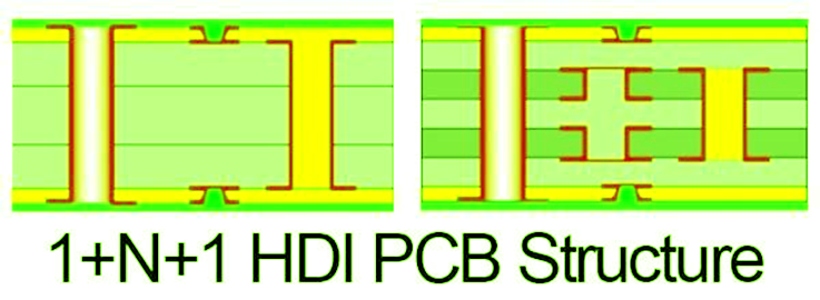
The HDI 1+N+1 structure represents the fundamental configuration for HDI (High-Density Interconnect) PCB. In this structure, both the first and last layers require blind hole drilling, typically accomplished through laser drilling techniques. These holes are primarily targeted in the area occupied by BGA (Ball Grid Array) components, while leaving sufficient space in other regions.
For 4 layer PCB, the configuration follows a sequence of 1-2 layer and 3-4 layer. Analogously, 6 layer board arrangement the layers as 1-2 layer and 5-6 layer. The notion of buried holes signifies that they are not visible from the outer layers, remaining concealed within the confines of the board.
HDI 1+4+1(6 Layer) Typical Stack up, without Buried Vias
The six-layer HDI PCB with a first-order design follows a 1+4+1 stack-up configuration, where the layers are organized as one core layer, four signal layers, and one additional core layer. Unlike through-hole boards, this design solely utilizes through holes and blind vias without any buried vias.
The production of HDI PCB necessitates specific processes, including press fitting, plating of blind vias, and through-hole formation. Compared to traditional multi-layer boards, HDI PCB require additional manufacturing steps such as laser drilling for blind vias.
In the scenario of a 1+4+1 stack up structure where buried holes are not found, the 1st and 3rd layers could be employed as a core board, with the 4th and 5th layers functioning as core board. The exterior layers are enhanced with a dielectric PP layer and a copper foil layer. These layers are laminated collectively, along with the insertion of the dielectric PP layer in the middle. This fabrication technique streamlines the PCB design, diminishes production expenses and trims down the entire production timeline.
HDI 1+4+1 Typical Stack-up, without Through Vias
To manufacture the 6-layer first-order blind buried via HDI PCB, two-step lamination process is employed. In the first lamination, the core layers are fused together and the buried vias are plated. Then, in the second lamination, resin is used to fill the blind vias. Finally, the blind vias are plated to establish electrical connections.
This HDI structure offers several benefits, including reduced costs and shorter delivery times. By eliminating the through-hole structure and employing blind and buried vias, the complexity of the PCB is minimized, resulting in more efficient production and cost savings.
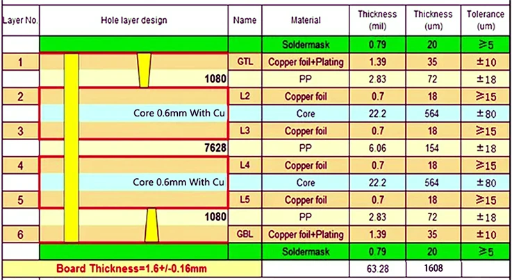
Standard 6 Layer HDI 1+4+1 Stack-up
The standard 6-layer HDI 1+ PCB board follows a stack up format of 1+N+1, where N is an even number greater than or equal to 2. This stack up configuration, consisting of 1 signal layer sandwiched between 4 internal signal layers and 1 final signal layer, is widely utilized in the industry as the mainstream design for 6-layer HDI PCB.
This particular board design incorporates various advanced features such as through-holes, buried vias and blind vias. The fabrication process of this 6-layer HDI 1+ PCB is quite complex, and involves multiple steps. It requires two pressings, wherein the layers are pressed together, followed by plating to establish the buried vias. Later, a resin plug assists in filling the holes, and a successive plating process is employed to develop the blind vias and through holes.
Design Guidelines for 1+N+1 HDI PCB
Designing 1+N+1 HDI High-Density Interconnect requires careful consideration of various factors to ensure successful implementation. Here are some important design guidelines to follow:
Layer Stack-up:
Optimize the layer stack up to accommodate the required signal, power, and ground planes while considering the space constraints. Utilize microvia technology, such as blind and buried vias, to achieve higher interconnect density.
Component Placement:
Plan component placement strategically to minimize signal path lengths, reduce crosstalk, and optimize thermal management. Consider the specific requirements of high-speed signals to maintain signal integrity, including signal vias and differential routing.
Routing Guidelines:
Follow proper routing guidelines to maintain signal integrity and minimize signal losses. Use controlled impedance routing for high-speed signals and differential pairs. Maintain appropriate spacing and clearance between different signal traces and critical components.
Power Integrity:
Ensure a well-designed power distribution network (PDN) to maintain power integrity. Use dedicated power and ground planes to minimize noise and achieve low impedance paths. Strategically place decoupling capacitors near critical components to suppress voltage fluctuations.
Thermal Management:
Consider thermal management techniques to dissipate heat effectively. Ensure an efficient thermal pathway by connecting thermal vias to heat sinks or ground planes. Distribute heat-generating components evenly to prevent localized hotspots.
Design for Manufacturing (DFM):
Collaborate with PCB fabricators and assembly houses to understand their manufacturing capabilities and limitations. Follow DFM guidelines to optimize the design for manufacturability, including proper clearances, minimum via sizes and panelization requirements.
EMI/EMC Considerations:
Pay attention to electromagnetic interference (EMI) and electromagnetic compatibility (EMC) issues. Minimize emissions by using proper grounding techniques, shielding and signal routing practices. Implement signal integrity measures to reduce susceptibility to external interference.
Design for Testability (DFT):
Incorporate features that facilitate testing and diagnostics, such as test points, access to critical signals, and built-in self-test (BIST) capabilities. Design the board in a way that allows for efficient debugging and troubleshooting during the manufacturing and assembly stages.
Documentation and Communication:
Maintain clear and comprehensive design documentation, including a detailed bill of materials (BOM) and assembly drawings. Communicate effectively with the manufacturer and assembly house to ensure a smooth transition from design to production.
Simulation and Validation:
Utilize simulation tools to analyze and validate the design, encompassing facets like signal reliability, power stability, thermal efficacy, and EMI/EMC attributes. Iterate and optimize the design based on simulation results to achieve desired performance.
These guidelines will help ensure the success of your 1+N+1 HDI PCB design, taking into account factors such as signal integrity, power integrity, thermal management, manufacturing considerations, and compliance with industry standards.
Manufacturing Process 1+N+1 HDI PCB
The methodology behind the crafting of 1+N+1 HDI PCB encompasses varied stages to obtain the anticipated extent of miniaturization and dense interconnection.
Design and Layout:
The design phase involves creating a detailed layout considering the specific requirements of the circuit, component placement, and signal routing.
High-density designs require careful consideration of trace widths, spacing, and via sizes to ensure signal integrity and manufacturability.
Substrate Preparation:
The manufacturing process begins with preparing the substrate material. Typically, high-performance materials like FR-4, FR-4 with high Tg (glass transition temperature), or specialized materials such as polyimide (PI) are used.
The substrate is cut into appropriate size panels according to the design requirements.
Inner Layer Processing:
The inner layer of the HDI PCB are independently processed, then collectively laminated to fabricate the multi-layered structure.
A thin layer of copper is applied onto both flanks of the inner layer panels via a procedure known as copper cladding.
The internal layers experience an array of procedures, encompassing the application of photoresist, exposure, and development to originate the sought-after copper traces and circuit schematics.
Laser Drilling:
Laser drilling is a critical step in the manufacturing of 1+N+1 HDI PCB. High-precision lasers are used to drill microvias and blind vias in the inner layers.
The drilled holes provide interconnection between the different layers and allow for the routing of traces in smaller areas.
Dielectric Layer Buildup:
The dielectric layers, typically made of epoxy resin and glass fiber, are built up on the inner layer panels. This buildup can be achieved using multiple lamination cycles or semi-additive processes, depending on the specific design requirements.
Plating and Copper Deposition:
After forming the dielectric layers, the panels go through a process called electroless copper plating. This involves the deposition of a thin layer of copper onto the inner walls of the drilled microvias and blind vias.
Subsequently, an additional layer of copper is electroplated onto the exposed copper surfaces to increase the thickness and electrical conductivity.
Outer Layer Processing:
The outer layer of the PCB is processed similarly to traditional PCB. This involves applying a photoresist layer, patterning the circuitry using photolithography techniques, and etching away the unwanted copper.
Surface Finish and Solder Mask Application:
A surface finish is applied to protect the exposed copper surfaces and facilitate component soldering. Common surface finishes include HASL (Hot Air Solder Leveling), ENIG (Electroless Nickel Immersion Gold), and OSP (Organic Solderability Preservative).
Finally, a solder mask is applied to cover the entire PCB surface, leaving openings for pad areas where components will be soldered.
Final Inspection and Testing:
The finished PCB undergo a thorough inspection and testing process to ensure quality and reliability. This includes checks for dimensional accuracy, circuit continuity, solderability and electrical performance.
Importance of 1+N+1 HDI PCB
The significance of 1+N+1 HDI PCB is anchored in their capacity to fulfill the growing demand for more compact, lightweight, and technically intricate electronic devices. Here are some principal factors elucidating the importance of 1+N+1 HDI PCB:
Miniaturization:
1+N+1 HDI PCB fosters the diminution in size of electronic instruments by authorizing surging circuit density and reducing the comprehensive dimensions of the PCB. This feature becomes pivotal for instances where spatial limitation is a chief determinant, such as in scenarios involving mobile contrivances, wearable technologies and IoT devices.
Increased functionality:
With the incorporation of high-density interconnections, 1+N+1 HDI PCBs initiate more intricate and progressive electronic designs. They offer the requisite routing abilities to host a more substantial count of components, engendering augmented functionality and facets in electronic apparatus.
Improved signal integrity:
HDI technology curtails the length of the signal pathway, thus mitigating signal losses, crosstalk, and electromagnetic interference. This contributes to enhanced signal integrity and elevated performance in high-velocity digital and RF applications.
Enhanced reliability:
The use of 1+N+1 HDI PCB can improve reliability in electronic devices. The reduced size and increased density minimize the number of interconnections, decreasing the probability of failure points. It also enables better thermal management and can help optimize the overall system reliability.
Cost optimization:
While 1+N+1 HDI PCB may have a higher initial cost compared to traditional PCB, their ability to reduce the overall size and weight of electronic devices can lead to cost savings in areas such as materials, manufacturing, assembly and transportation.
Limitations and Challenges of 1+N+1 HDI PCB
In relation to 1+N+1 HDI High-Density Interconnect, specific limitations and challenges warrant consideration. Here are a few common instances:
Complexity and Design Constraints:
The design of 1+N+1 HDI PCB can be significantly more intricate compared to standard PCB. The escalated density and diminution necessitate meticulous contemplation of routing, layer stack-up and component placement. Designers need to deal with tight design constraints, such as trace widths, spacing and pad sizes, which can be challenging.
Manufacturing Processes:
The 1+N+1 HDI PCB frequently necessitate cutting-edge manufacturing techniques like laser drilling, sequential buildup, and multiple lamination stages. These processes can be more expensive and time-consuming compared to standard PCB manufacturing, adding to the overall production cost and lead time.
Cost:
The execution of 1+N+1 HDI PCB may command a higher expense compared to conventional PCB, attributable to the complexity of the design and manufacturing process. The higher complexity and specialized processes involved can increase material costs, fabrication costs and assembly costs.
Signal Integrity and Electromagnetic Interference (EMI):
As the density of components and interconnections increase in 1+N+1 HDI PCB, signal integrity and EMI become more significant concerns. Careful layout and routing techniques need to be employed to mitigate signal integrity issues such as impedance mismatches, signal reflections, and noise coupling.
Thermal Management:
Higher circuit density in 1+N+1 HDI PCB can lead to increased heat dissipation challenges. Efficient thermal management becomes critical to prevent overheating and ensure the long-term reliability of the electronic components.
Reliability and Repairability:
The miniaturization and complexity of 1+N+1 HDI PCB can make them more challenging to repair and troubleshoot in case of failure. Accessibility to individual components and repair points may be limited, requiring specialized equipment and expertise.
Testing and Inspection:
The dense layout and multiple layers of 1+N+1 HDI PCBs can make testing and inspection processes more challenging. Extra care and sophisticated testing methods may be necessary to ensure thorough functionality testing and quality control.
Despite these limitations and challenges, the advantages like miniaturization, augmented functionality, and enhanced signal integrity render 1+N+1 HDI PCB an inescapable necessity for numerous sophisticated electronic applications. With technological progression and the industry’s ceaseless innovation, initiatives are being undertaken to confront and surmount these challenges in 1+N+1 HDI PCB design and fabrication.
To Sum Up
HDI PCB technology performs a crucial part in facilitating the formation of miniaturized electronics through the integration of compact interconnections, slight characteristics, and slender materials. As the call for less bulky and lighter articles rises, HDI delivers a solution to lodge a superior quantity of functionalities and components in restricted areas.
1+N+1 HDI boards are widely employed in the production of printed circuit boards, particularly when dealing with a BGA (Ball Grid Array) pitch of 0.5. These boards are specifically utilized when the thickness of the HDI circuit board FR4 sheet is equal to or less than 4 mil. In the case of utilizing PP (Prepreg) material, it is generally recommended to use 1080, while avoiding the usage of 2116 PP whenever possible.
When patrons do not establish particular prerequisites, it is desirable to employ 1OZ copper foil on the internal layer of conventional PCB. Conversely, for HDI boards, the use of HOZ copper foil is advocated, with 1/3OZ copper foil finding favor for the internal and external electroplating layers. These directives are intended to guarantee optimal performance and alignment with the stated specifications. As a professional PCB fabricator, we give precedence to the utilization of suitable materials and methodologies to conform to the apex industry thresholds.


