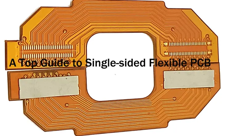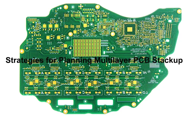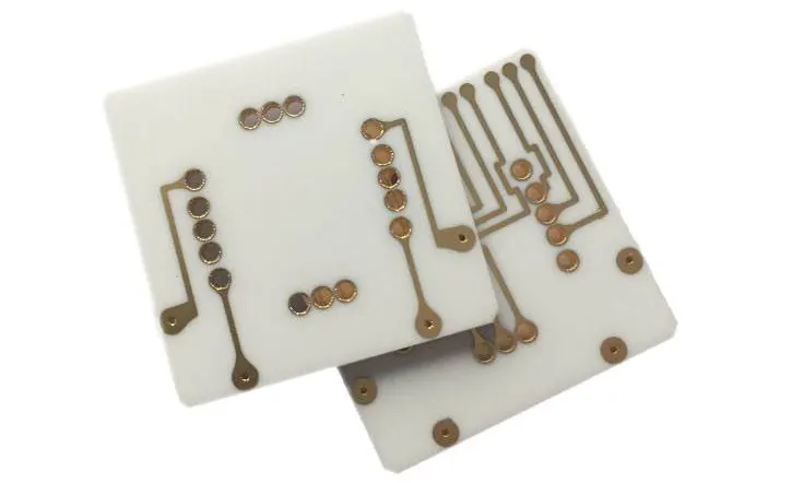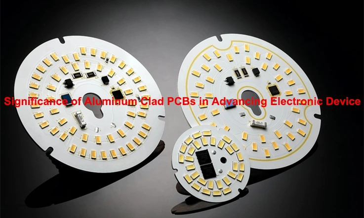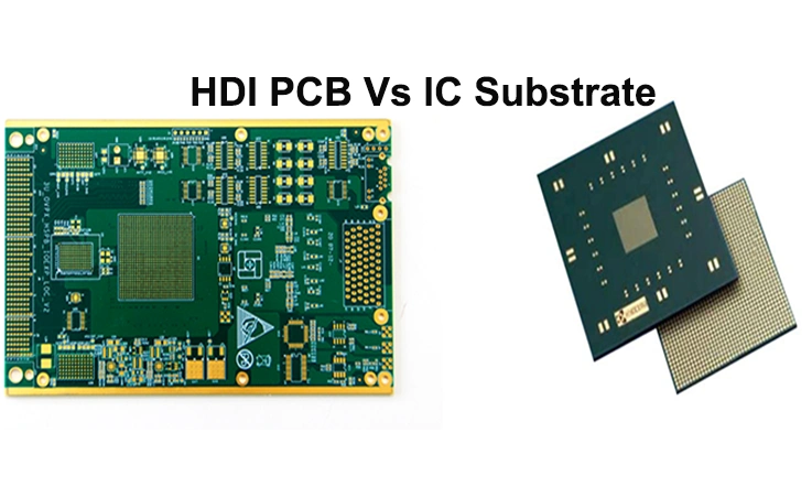
HDI PCBs and IC substrates differ in structure, process flow, and application. We presents a detailed technical comparison based on seven core areas: material systems and structural differences, design workflows and software ecosystems, testing methodologies, cost models, assembly integration strategies, industry compliance, and ongoing trends in miniaturization. HDI PCB topics include stackup strategies, mSAP and aSAP fabrication, embedded passives, crosstalk mitigation, and yield-focused optimization. On the IC substrate side, the focus shifts to RDL fan-out evolution, embedded bridge technology, JEDEC-compliant warpage control, and challenges in high-volume production.
Overview of HDI PCB and IC Substrate Technologies
Modern electronic systems demand progressively denser packaging and advanced interconnect strategies. This necessity drives two distinct but intersecting technologies: High-Density Interconnect (HDI) PCBs and IC Substrates. While both involve multilayer constructions and microfabrication techniques, their design objectives, material requirements, and manufacturing complexity differ substantially. Understanding the nuances between them isn’t just academic—it informs better design decisions and product optimization, especially when system performance, miniaturization, and manufacturability are on the table.
Let’s break it down and see where these two technologies align, where they diverge, and how they’ve come to occupy unique places in electronics assembly and semiconductor packaging.
What is HDI PCB?
Structure, Materials, and Manufacturing Approach
High-Density Interconnect PCBs are built for compact, high-performance devices. These boards typically feature:
●Laser-drilled microvias, stacked or staggered for multilayer interconnects
●Build-up layers using sequential lamination
●Resin-coated copper foils (RCC), BT epoxy, and FR-4 variants like ITEQ IT-988G SE
●Minimum line/space often below 75µm, pushing the limits of traditional PCB design
●High-Tg and low Dk/Df materials, such as Isola IS420 or Panasonic MEGTRON series
| Feature | Typical HDI PCB Range |
| Line/Space | 50–100µm |
| Dielectric Constant (Dk) | 3.5–4.2 |
| Glass Transition Temp (Tg) | 170–250°C |
| Copper Weight | 0.5–1 oz per layer |
Manufacturing calls for laser drilling, semi-additive processing (SAP), and often via-in-pad configurations. One of the upsides is its scalability—HDI technology allows designers to push boundaries without switching to wafer-level packaging.
Still, the complexity ramps up with via stacking and material compatibility, especially when dealing with multiple lamination cycles and high aspect ratios. Manufacturers often juggle IPC-2226 Class II and III guidelines while also tuning for thermal management and signal integrity.
What is an IC Substrate?
Layer Architecture, Resin Systems, and Performance
Unlike HDI PCBs, IC substrates serve as bridges between semiconductor dies and PCBs. They’re thinner, denser, and often produced in panelized formats using substrate-like PCB (SLP) fabrication or build-up methods aligned with semiconductor process nodes.
Core attributes include:
●ABF (Ajinomoto Build-up Film) or polyimide resin systems
●Ultra-fine pitch (≤15μm/15μm) line/space
●Low CTE base materials to align with die shrinkage/expansion
●Ni/Au or ENEPIG surface finishes, optimized for wire bonding or flip-chip
| Metric | IC Substrate Typical Value |
| Layer Count | 4–18 |
| Minimum Trace Width | 5–15μm |
| Dielectric Constant | 3.0–3.6 |
| Thickness | <0.4mm total |
IC substrates shine in environments where chip-scale packaging (CSP), BGA, and flip-chip assemblies are involved. Companies like Shinko Electric, Ibiden, and Kinsus dominate this space, offering ABF-based substrate services tailored for high-pin-count applications.
Manufacturing involves SAP or mSAP (modified semi-additive process), desmear, and plasma cleaning. Quality control measures such as AOI, X-ray inspection, and warpage control are stricter than traditional PCB processes due to the tight tolerances and thermal cycling considerations.
Substrate Materials and Core Laminates
When comparing HDI PCBs and IC Substrates, the base material selection is more than a technical preference—it influences layer configuration, thermal response, mechanical stability, and long-term reliability under repeated assembly cycles. Material systems define not only performance margins but also how these products behave during laser drilling, sequential lamination, and metallization. This section analyzes core substrate materials used in both HDI and IC Substrate technologies, focusing on resin chemistry, thermal properties, and dielectric performance.
Resin Systems in HDI PCBs: FR4, BT, and Polyimide Analysis
HDI PCB designs typically incorporate resin systems chosen to align with specific structural and processing targets:
●FR4 Epoxy Systems: Frequently used in HDI stackups such as 1+N+1 or 2+N+2 configurations. These systems are compatible with conventional PCB lamination and drilling processes. However, their higher dielectric loss and relatively moderate thermal stability may limit signal integrity in high-frequency domains.
●BT Epoxy (Bismaleimide-Triazine): Selected for enhanced moisture resistance and better dimensional control during thermal excursions. BT-based materials often appear in portable electronic modules requiring higher reliability margins and improved electrical insulation.
●Polyimide: Recognized for its thermal endurance and mechanical strength. Polyimide-based HDI PCBs are frequently used in applications with sustained high temperatures or exposure to aggressive reflow cycles. Despite its benefits, polyimide’s higher CTE may require additional compensation during via stacking and registration alignment.
Each resin system impacts reliability outcomes and processing strategies differently. Understanding the resin behavior under multiple press cycles or chemical exposure is must during early material selection and stackup design.
IC Substrate Materials: Ajinomoto Build-up Film (ABF) and Epoxy Resins
IC Substrates prioritize materials that support fine-line imaging, dielectric stability, and compatibility with flip-chip packaging:
●Ajinomoto Build-up Film (ABF): Widely implemented in FC-BGA and SiP packages. ABF resins are tailored for ultra-fine line etching and laser drill compatibility. Their uniform dielectric properties make them suitable for routing below 5 µm line/space dimensions.
●Epoxy Resin Coated Copper (RCC): RCC is a lower-cost alternative to ABF, with reasonable thermal and dimensional performance. RCC materials are often used in chip substrate configurations that don’t demand ultra-fine features but still require consistent lamination results and metallization adhesion.
The choice between ABF and epoxy RCC is generally guided by the pitch of the silicon die, I/O count, and the packaging house’s process window. These materials also influence signal skew, thermal expansion matching, and solder joint stability during underfill and final assembly.
Dielectric Properties, Tg, and CTE Comparisons Between HDI PCB and IC Substrate
Material behavior under thermal and electrical stress is fundamental to both HDI and IC Substrate design. Core comparative parameters include:
●Dielectric Constant (Dk): FR4 materials typically range between 4.2 and 4.5, whereas BT epoxies may fall below 4.0. ABF substrates usually offer Dk values around 3.0–3.3, allowing tighter impedance control and less signal delay at higher frequencies.
●Dissipation Factor (Df): FR4 often exceeds 0.015, while BT epoxy falls near 0.010. ABF can perform below 0.008, which reduces signal attenuation in high-speed routing.
●Glass Transition Temperature (Tg): Standard FR4 may exhibit Tg between 130–170°C. BT resin can reach 180–200°C. ABF films usually exceed 210°C, providing more dimensional stability during lead-free solder reflow.
●Coefficient of Thermal Expansion (CTE): HDI PCBs tend to exhibit Z-axis CTE values in the 50–70 ppm/°C range, while ABF materials are usually more tightly controlled below 45 ppm/°C. This difference supports tighter integration with silicon dies and reduces risk during thermal excursions.
Material metrics such as Dk, Df, Tg, and CTE are not theoretical benchmarks—they directly influence line impedance, via reliability, and board-level warpage. Matching material properties with expected signal speeds and thermal profiles should be part of every design review process.
Layer Structure and Via Formation
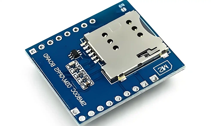
Understanding how HDI PCB and IC Substrate technologies manage their layer architecture and via formation processes is fundamental when evaluating performance under assembly stress, design complexity, and form factor constraints. These structures shape trace routing, electrical isolation, via density, and interconnection reliability. This section outlines how microvias, build-up layers, and coreless techniques are applied across both technologies and how via reliability is influenced by drill processes and thermal load exposure.
Microvias and Blind/Buried Vias in HDI PCB Stack-ups
HDI PCB designs typically rely on stacked or staggered microvia structures to maintain signal integrity and density within compact footprints. Here’s how they’re commonly implemented:
●Microvia Characteristics: These laser-drilled vias typically penetrate one dielectric layer and connect adjacent copper layers. Microvias support fine-line routing with line/space below 75 µm and enable denser interconnects than traditional plated through-hole (PTH) designs.
●Blind and Buried Vias: Blind vias connect outer layers to inner ones without penetrating the full board. Buried vias connect two or more internal layers. When paired strategically with microvias, they support structures such as 1+N+1 to 7+N+7, where “N” indicates the number of core layers.
●Sequential Lamination: Each additional via layer often requires a separate lamination cycle. Misalignment, resin flow, and copper expansion must be managed during each step to ensure vertical via integrity.
Table: Microvia and Lamination Characteristics in HDI PCB
| Structure Type | Typical Diameter | Stack Configuration | Lamination Cycles | Usage Example |
| Microvia | 50–100 µm | Stacked/Staggered | 1 per microvia layer | Mobile sensors, RF PCBs |
| Blind Via | 100–200 µm | Outer to inner layers | 1 | Wearables, compact boards |
| Buried Via | 100–200 µm | Internal-only | 1 | High-density core transitions |
For example, a typical HDI PCB used in wearable sensor modules may have 2+N+2 stack-up with stacked microvias filled with conductive paste and plated to achieve a robust interconnect path.
Build-up Layers and Coreless Structures in IC Substrates
IC Substrates differ from HDI PCBs by emphasizing ultra-thin build-up layers and often omitting conventional cores. These configurations are optimized for semiconductor packaging needs:
●Build-up Dielectrics: Using materials like Ajinomoto Build-up Film (ABF), these ultra-thin dielectrics support multiple layers below 50 µm thickness. The uniformity enables finer lines and tighter via pitch, frequently required in flip-chip ball grid array (FC-BGA) packaging.
●Coreless Lamination: Many IC Substrate designs eliminate rigid cores and instead use temporary carriers during processing. Once build-up layers and circuitry are completed, the carrier is removed. This enables thinner, more flexible substrate designs for advanced packages.
●Interconnect Density: IC Substrate configurations often achieve L/S (line/space) ratios below 10/10 µm. To manage this, subtractive etch, semi-additive processes (SAP), and modified semi-additive processes (mSAP) are often used in tandem with laser via formation.
These techniques are common in CPU, GPU, and SoC packaging platforms where die pitches are low, and the interconnection strategy must support both routing and heat dissipation.
Via Reliability, Drill Technology, and Reflow Performance
Both HDI PCBs and IC Substrates require reliable via structures that can withstand reflow processes, high temperature cycling, and mechanical stress without delamination or crack propagation:
●Laser vs. Mechanical Drilling: HDI PCBs often use CO₂ or UV laser drilling for microvias due to their precision and minimal resin damage. IC Substrates typically rely on laser-based ablation due to the small via diameter required for sub-20 µm features.
●Via Filling Techniques: HDI PCBs frequently utilize copper electroplating or conductive paste filling. IC Substrates lean toward thin copper plating using mSAP or SAP for better dimensional control and smoother via walls.
●Reflow and Thermal Cycling: During SMT processes, vias are exposed to multiple reflow cycles, especially for BGAs and CSPs. Poor via fill, mismatch in CTE (Coefficient of Thermal Expansion), or incomplete adhesion may lead to reliability issues like via cracking or barrel fracture.
Table: Via Reliability Factors Across Platforms
| Parameter | HDI PCB | IC Substrate |
| Drill Type | CO₂ or UV Laser | Laser Ablation |
| Via Diameter | 50–100 µm | 10–30 µm |
| Fill Material | Conductive paste / Cu plating | Thin Cu plating (SAP/mSAP) |
| Typical Failures | Copper barrel cracks, voids | Microvoids, adhesion failure |
| Reflow Stress Tolerance | Moderate (2–3 cycles at 245–260°C) | High (up to 5 cycles at 260°C) |
For instance, in a four-layer HDI PCB deployed in mobile applications, reflow-induced failures often stem from insufficient copper thickness or via misalignment. In contrast, ABF-based IC Substrates used in high-end SoCs focus on suppressing microvoids during plating and optimizing lamination cycles to limit thermomechanical strain.
Surface Finish Technologies
Surface finishes in HDI PCB and IC Substrate production are closely tied to performance targets such as pad flatness, corrosion resistance, solder joint consistency, and high-frequency signal integrity. The finish applied can influence both yield during assembly and electrical stability during operation. This section examines commonly used surface treatment techniques across HDI PCB and IC Substrate applications, focusing on solderability, pad compatibility, and surface morphology in the context of multilayer routing and fine-line architectures.
ENIG, OSP, and Immersion Silver for HDI PCB Manufacturing
In HDI PCB fabrication, finishes are selected based on assembly method, pad design, and thermal profile. Each technique supports different design needs and handling conditions:
●ENIG (Electroless Nickel Immersion Gold) provides a dual-layer metallic finish—nickel acts as a barrier to copper diffusion, while the gold layer guards against oxidation. This process is typically used for HDI designs with BGA components and fine-pitch layouts due to its planarity and wetting characteristics. However, “black pad” concerns from sulfur contamination necessitate process control.
●OSP (Organic Solderability Preservative) uses an organic layer to preserve copper surfaces from oxidation prior to soldering. It’s often used in HDI builds requiring low-cost, lead-free processes. The trade-off includes limited thermal cycles and sensitivity to multiple reflows.
●Immersion Silver delivers a flat, solderable surface with excellent conductivity. It’s frequently applied in RF-centric HDI PCBs where impedance consistency is expected. Attention is needed to avoid silver migration in high-humidity environments.
IC Substrate Surface Finishes: Flash Gold and Electroless Plating
IC Substrates handle extremely dense pad arrays, demanding finishes that maintain planarity and bondability across narrow geometries:
●Flash Gold involves applying a thin gold layer (often < 0.1 µm) over nickel to prevent oxidation and allow for consistent wire bonding. It’s widely used for microbump or wire bond areas in IC Substrates due to its thin, uniform deposit.
●Electroless Plating, such as Ni/Au or Ni/Pd/Au, coats pads without external electrical current, ensuring even distribution across tight-pitch contacts. Ni/Pd/Au finishes also reduce the risk of corrosion and enhance ball grid array soldering reliability in flip-chip applications.
For instance, flip-chip packaging substrates for SoCs typically adopt electroless Ni/Pd/Au to ensure stable mechanical bonding and controlled resistance across thousands of I/O pads.
Surface Roughness, Bonding, and Signal Integrity Considerations
Surface texture and metallurgical bonding contribute to more than visual quality—they can shape high-speed electrical behavior and thermal stability:
●Surface Roughness (Ra/Rq): Lower roughness reduces conductor loss at high frequencies. Immersion silver and ENIG provide smoother surfaces than OSP, enabling tighter impedance control in HDI signal lines. In IC Substrates, surface roughness under 0.3 µm is usually targeted, particularly for fine-pitch packages exceeding 20 Gbps.
●Bond Strength and Delamination: Reliable finishes improve mechanical attachment during soldering and wire bonding. Electroless finishes maintain strong adhesion through multiple reflow cycles, reducing the likelihood of intermetallic cracking.
●Signal Integrity: Surface finish affects insertion loss and return loss. For example, in HDI PCBs used in data signal routing beyond 10 GHz, immersion silver enables flatter response curves by reducing surface-induced impedance shifts.
Signal Integrity and High-Speed Performance
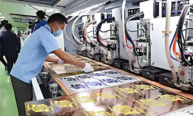
As the demands for high-speed digital and RF performance increase across multilayer electronic assemblies, maintaining signal clarity becomes a front-and-center design consideration. In both HDI PCB and IC Substrate technologies, layout, material selection, and structural configuration directly affect the transmission quality of high-frequency signals. Each platform addresses signal performance with distinct strategies that reflect their unique use cases. Let’s dig into the core technical aspects that influence high-speed behavior.
HDI PCB Design for High-Frequency Applications
HDI PCB layouts tailored for high-speed operation typically leverage fine-line trace routing, controlled impedance layers, and optimized via transitions. These elements reduce parasitics and help maintain waveform integrity across the board.
●Tightly controlled impedance:Stackups with defined prepregs and copper thicknesses are configured to support controlled impedance requirements in interfaces such as PCIe, HDMI, and USB.
●Via stub reduction: Techniques such as backdrilling and laser-drilled microvias remove unnecessary copper from via barrels, limiting signal reflection and loss.
●Material selection: For HDI boards used in GHz-frequency environments, low-loss materials like Megtron 6 or Panasonic R-5775 series are selected for their stable dielectric constants and low dissipation factors.
Table: Typical HDI PCB High-Frequency Parameters
| Parameter | Value/Range | Example Materials |
| Trace width (controlled) | 60–90 µm | Standard 50 Ω designs |
| Impedance tolerance | ±10% | PCIe Gen4/Gen5 interfaces |
| Dielectric constant (Dk) | 3.4–3.8 | Megtron 6, R-5775 |
| Loss tangent (Df) | ≤ 0.004 | Rogers 4350B |
| Via stub length | < 150 µm (post-backdrill) | Laser-drilled microvias |
Designers aiming for tight signal margins will find that microvia-in-pad routing, thinner dielectric layers, and clean reference planes help reduce skew and timing mismatches, even in space-constrained applications.
IC Substrate Signal Loss, Crosstalk, and Impedance Control
IC Substrates support advanced packaging demands by enabling sub-100µm routing and ultra-short interconnects directly underneath the die. Here, signal performance isn’t just about board-level communication—it’s also about die-to-die and die-to-ball interfaces operating at tens of gigabits per second.
●Substrate trace dimensions: With trace widths often below 10µm, crosstalk and coupling are mitigated using embedded reference planes and tightly tuned dielectric constants.
●Build-up layer uniformity: ABF (Ajinomoto Build-up Film) provides uniform dielectric spacing, which supports consistent impedance behavior across flip-chip interfaces.
●Electromagnetic shielding: Embedded ground mesh or patterned ground shields within the substrate suppress unwanted coupling in dense BGA layouts.
Table: Typical IC Substrate High-Speed Characteristics
| Feature | Specification | Material/Process |
| Trace width | 5–10 µm | SAP (Semi-Additive Process) |
| Line-to-line spacing | 5–10 µm | ABF-based core builds |
| Dielectric constant (Dk) | 3.0 ± 0.1 | Ajinomoto ABF GX-92R |
| Loss tangent (Df) | ≤ 0.0025 | ABF GX series |
| Insertion loss (10GHz) | < –1.5 dB/inch | 2.5D/3D Interposer |
With routing under 10 µm and ultra-short signal distances, IC substrates accommodate data rates exceeding 56 Gbps while managing insertion loss and eye diagram degradation.
Dielectric Constant and Loss Tangent Behavior in Advanced Packaging
The performance of high-speed circuits hinges on the stability and frequency-dependence of dielectric properties like Dk (dielectric constant) and Df (dissipation factor or loss tangent). These values shape how well a signal is preserved as it propagates through a material.
●HDI PCB materials: Advanced FR4 variants or high-frequency laminates like Rogers 4350B maintain consistent Dk (~3.5–3.8) across wide frequency ranges with Df below 0.004.
●IC substrate materials: ABF resins typically offer Dk values near 3.0 with lower loss tangents at millimeter-wave frequencies, suitable for multi-chip modules and high-speed SerDes.
Table: Comparative Dielectric Properties for HDI vs IC Substrate
| Material Type | Dk (10GHz) | Df (10GHz) | Application Scope |
| Rogers 4350B | 3.66 | 0.0037 | RF/microwave HDI PCBs |
| Panasonic Megtron 6 | 3.4 | 0.002 | High-speed digital HDI |
| Ajinomoto ABF GX-92R | 3.05 | 0.0022 | 2.5D/3D IC Substrate packaging |
| SLC Interposer Laminate | 2.9–3.1 | 0.0020–0.0025 | Advanced flip-chip & SiP substrates |
Design selection should factor in loss modeling, dielectric stability over temperature, and S-parameter validation. For GHz-bandwidth circuits, maintaining dielectric homogeneity over thousands of interconnects can significantly reduce bit error rates and jitter accumulation.
Thermal Management and Reliability Considerations
Effective thermal design and long-term mechanical stability are two areas where HDI PCB and IC substrate technologies follow different engineering philosophies. HDI PCB designs are often aligned with system-level heat dissipation requirements, while IC substrates must manage concentrated thermal loads in ultra-dense footprints. The following sections explore how each platform addresses thermally induced stress, expansion mismatch, and structural endurance across multiple thermal cycles.
Thermal Conductivity and Dissipation in HDI PCBs
In HDI PCB fabrication, managing thermal conductivity is not just a matter of selecting the right copper weight or laminate—it involves a combination of layer design, via optimization, and resin system selection. FR4-based systems, while common, often require supplementary features like thermal vias or embedded metal cores to direct heat away from active components. Polyimide-based HDI structures offer improved thermal pathways due to their resin formulation but bring challenges in dimensional control.
Designers typically:
●Add thermal vias below power ICs to minimize local hot spots.
●Use thicker copper layers in power planes to increase lateral heat spreading.
●Choose resin systems with tailored thermal conductivity values (e.g., 0.6–1.2 W/m·K).
This approach allows HDI PCBs to function reliably in multi-board assemblies where consistent heat dissipation is necessary. Overlooking this step can easily cause hot spots that shorten component lifespan or trigger unpredictable electrical behavior.
Warpage Control and Thermal Expansion in IC Substrates
IC substrates, especially those employing Ajinomoto Build-up Film (ABF) or modified epoxy resins, require precise warpage management due to their thin profile and fine-pitch interconnects. These structures must maintain dimensional stability through reflow processes and long-term device operation.
Main methods for thermal expansion control include:
●Using coreless constructions or symmetric layer stacks to counteract warpage.
●Engineering CTE-matched dielectric materials to reduce stress between the silicon die and substrate.
●Incorporating copper-invar-copper (CIC) layers for dimensionally stable reinforcement.
For example: substrates used in flip-chip BGA packages often operate within ±0.02 mm warpage limits after lead-free reflow, demanding careful tuning of glass transition temperatures (Tg) and coefficient of thermal expansion (CTE) across every layer.
Reliability Testing: IST, CAF Resistance, and Reflow Survivability
Reliability validation in both HDI PCB and IC substrate fabrication spans several standardized test methods. Interconnect Stress Testing (IST) is used widely to simulate cyclic thermal stress on plated through-holes and microvias, while Conductive Anodic Filament (CAF) resistance checks insulation performance under bias and humidity.
HDI PCBs are often tested through:
●IST up to 1500 cycles for stacked microvia robustness.
●CAF exposure at 85°C/85% RH under 100V bias.
●Thermal shock from −40°C to +125°C in 500-cycle increments.
IC substrates follow similar protocols but face tighter failure thresholds, especially due to thinner dielectric spacing and finer trace width. Reflow survivability testing for substrates is also stricter, often requiring three consecutive lead-free reflow simulations without measurable delamination, blistering, or warpage beyond IPC-defined limits.
Design Considerations about HDI PCB and IC Substrate
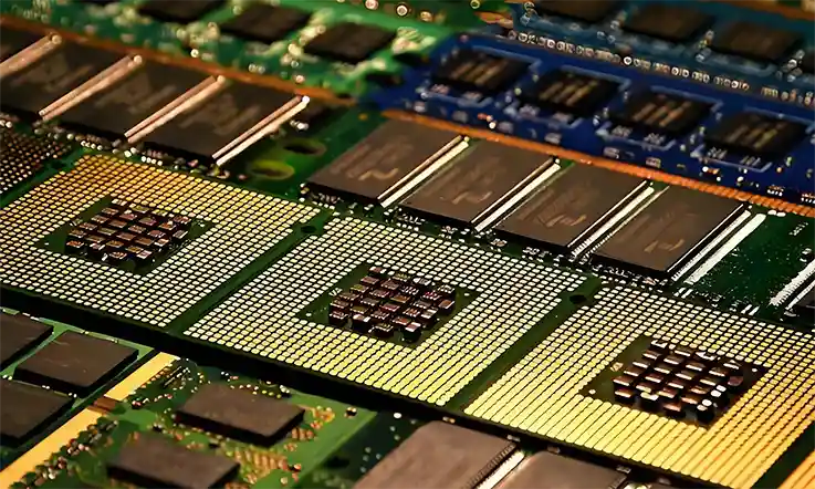
When evaluating HDI PCB and IC substrate design strategies, several technical variables must be addressed early in the planning phase. These include material selection, layout constraint handling, impedance models, and compatibility with high-frequency signals. Design tools for both domains are built to handle increasing interconnect density, signal fidelity needs, and manufacturing limitations, but they differ substantially in stack-up rules, spacing guidelines, and simulation depth.
By understanding these design flows and tool-specific requirements, layout professionals can establish performance baselines, streamline prototyping, and reduce design iterations.
HDI PCB Design Flow: Stackup, Constraints, and DRC Rules
Designing HDI PCBs begins with defining layer stack-ups that include build-up layers, microvias, and blind/buried interconnect schemes. These multilayer configurations are selected based on routing density, controlled impedance channels, and copper thickness considerations.
●Layer Stack-Up Planning: Typically includes 1+N+1 to 7+N+7 configurations, enabling microvias to connect build-up layers to a central core.
●Design Rule Constraints: Spacing, trace width, via pad size, and aspect ratios are defined based on fabrication capabilities. EDA tools use constraint-driven layouts to auto-check violations.
●DRC and DFA Integration: Most HDI layouts integrate Design Rule Checking (DRC) and Design for Assembly (DFA) into early layout stages using software like Altium Designer, Allegro, or OrCAD.
IC Substrate Design Tools: Cadence, Mentor, and ANSYS
IC substrates require design approaches that accommodate fine-line routing, padless via structures, and substrate-layered signal redistribution. Design software used in IC packaging environments often incorporates physical verification, thermal modeling, and SI/PI co-simulation modules.
●Cadence Allegro Package Designer Plus: Supports flip-chip bump placement, substrate via modeling, and under-bump metallization planning.
●Mentor Xpedition Substrate Integrator: Offers 3D package modeling, rule-driven interconnects, and bond-wire placement modeling.
●ANSYS Siwave and HFSS: Used for signal integrity and electromagnetic simulation with full-wave solvers for high-speed trace modeling.
Layout Optimization for Crosstalk, EMC, and High-Speed Signals
In both HDI PCBs and IC substrates, managing electromagnetic coupling, impedance discontinuities, and ground return paths is essential to preserve signal clarity. Mismanagement of these factors may lead to signal degradation or functional failure during validation.
●Crosstalk Minimization: Achieved by enforcing line-spacing rules and orthogonal trace routing between adjacent layers.
●EMC Compliance: Shielding layers, power-ground plane pairing, and decoupling capacitor placement are tuned during layout.
●High-Speed Routing Rules: Length matching, differential pair tuning, and stub minimization are standard in DDR, PCIe, and SerDes layouts.
Manufacturing Complexity and Yield Management
As design rules tighten and interconnect densities increase, both HDI PCBs and IC substrates present challenges in process control, defect reduction, and dimensional accuracy. Each technology relies on specific manufacturing workflows that directly impact yield, throughput, and inspection methodologies. This section dissects these challenges across fabrication stages, highlighting methods used in managing registration errors, warpage, sub-micron pattern fidelity, and defect identification.
HDI PCB Production Challenges: Registration, Etching, and Yield
High-Density Interconnect PCBs require multiple cycles of layer build-up and laser drilling. This introduces cumulative registration deviation and places emphasis on etching fidelity, pad alignment, and copper thickness control.
●Laser via alignment: During sequential lamination, misalignment can occur between stacked microvias and underlying pads. Advanced optical registration systems with sub-10 μm accuracy help maintain inter-layer consistency.
●Etch uniformity: Features below 100 μm demand controlled etching to prevent trace width loss or undercutting. Process tuning is necessary to preserve impedance and trace density across the panel.
●Yield impact: Defects such as open vias, copper voids, and dielectric delamination directly influence pass rates. Yield is managed through SPC tools and in-line defect tracking software.
HDI fabrication thrives on high first-pass yield. Precision equipment and calibration cycles reduce variation, while AOI and flying probe testers assist with pre-lamination defect detection. For scalable production, understanding drill-to-copper spacing and pad-to-via tolerances can go a long way toward stabilizing output. Start optimizing your line by reviewing via registration maps and layer misalignment reports.
IC Substrate Fabrication: Sub-Micron Tolerance and Substrate Warpage
IC substrates support multi-chip modules and wafer-level packaging. The fine features often fall below 15 μm line/space, requiring panel or strip-based processing with extremely tight tolerances.
●Build-up accuracy: ABF films and modified epoxy systems require controlled lamination with ±5 μm tolerance. Dry-film patterning and semi-additive processing (SAP) are used to form sub-micron traces.
●Warpage management: Differential expansion from copper and dielectric materials introduces board-level distortion during reflow. Warpage control involves coreless designs, filler systems, and reflow profile tuning.
●Dimensional stability: Substrate fabrication depends on low CTE values, resin shrinkage control, and glass weave alignment to maintain copper-to-pad precision across multiple layers.
Consistent quality in IC substrates is achieved through high-resolution patterning tools like LDI (Laser Direct Imaging) and X-ray alignment stages. Panel warpage is mitigated using stress-balanced stack-ups and pre-bake processes. Consider a review of lamination profiles and thermal distortion simulations to cut down rework cycles.
AOI, SEM, and Yield Analysis in Advanced Interconnect Substrates
Yield management in both HDI PCBs and IC substrates relies on high-resolution inspection systems. As feature sizes shrink, conventional inspection methods are supplemented by more advanced techniques.
●Automated Optical Inspection (AOI): Used post-etch and post-drill for via alignment, copper residue, and line breaks. In IC substrates, AOI resolution must exceed 1 μm to detect micro-bridge or open defects.
●Scanning Electron Microscopy (SEM): Deployed in failure analysis, especially for defect localization in underfill regions or micro-crack detection in interlayer vias.
●Yield metrics: Metrics such as first-pass yield, defect density (defects/cm²), and escape rate guide process decisions. Overlay analysis and defect pareto charts help track upstream contributors.
Electrical Test Strategies and Inspection
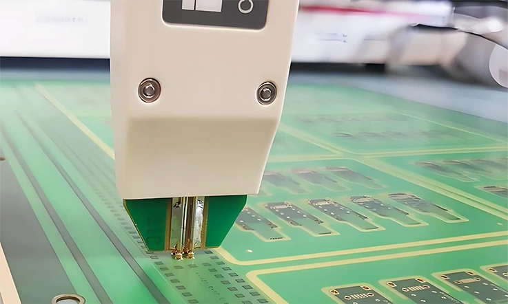
Ensuring signal performance, power distribution accuracy, and minimal electromagnetic interference requires meticulous inspection and testing throughout the HDI PCB and IC substrate manufacturing processes. As complexity in interconnect density increases, so does the necessity to apply differentiated test strategies. From flying probe tests on high-density interconnect PCBs to probe card techniques on fine-pitch IC substrates, electrical test methodologies directly affect the ability to evaluate open/short circuits, impedance control, and layout fidelity. The following sections outline distinct approaches used in both platforms and elaborate on their functional implementations in production settings.
HDI PCB Electrical Testing: Flying Probe vs. Bed-of-Nails
HDI PCBs often integrate blind and buried vias, microvias, and ultra-thin traces. As a result, electrical testing strategies must accommodate reduced pad sizes and multilayer routing. Two mainstream approaches include:
●Flying Probe Testing: Applied in low-to-mid volume production or during prototype validation, flying probe systems offer flexibility in accessing a wide range of test points without the need for dedicated fixtures. Precision probe positioning systems combined with vectorless testing enhance the ability to assess net connectivity, though test speed may be limited.
●Bed-of-Nails Fixtures: In higher-volume scenarios, fixture-based testing can offer throughput advantages. Rigid pins simultaneously contact multiple test nodes, delivering rapid assessment of opens and shorts. However, fixture fabrication time and cost increase with layer count and test point density.
Table: HDI PCB Electrical Testing Comparison
| Test Method | Application Scope | Test Resolution | Speed | Fixture Required | Typical Use Case |
| Flying Probe | Prototypes to mid-volume | ~50 µm | Moderate | No | Flexibility for varied designs |
| Bed-of-Nails Fixture | High-volume, stable designs | ~75–100 µm | High | Yes | Cost-effective in mass production |
Performance validation is further enhanced using controlled impedance testing modules, especially for designs above 2 GHz. Many designers frequently collaborate with CAM teams to ensure test pads and breakouts meet the electrical contact criteria for target test configurations.
IC Substrate Testing: Probe Cards, EDA Tools, and Bare Die Inspection
IC substrates, characterized by fine-line patterning, multi-depth vias, and ultrathin dielectrics, require a different approach to electrical evaluation. The process typically includes:
●Probe Cards: Customized probe cards interface with substrate test pads to perform die-level parametric testing. These cards can handle pad sizes in the range of 20–40 µm and pitch values below 100 µm, suitable for advanced packaging architectures like flip-chip or 2.5D interposers.
●EDA-Based Inspection: Electronic Design Automation (EDA) verification ensures that layout-to-mask to final substrate alignment is maintained. DRC and LVS checks during tape-out enable earlier detection of trace width violations or misaligned redistribution layers.
●Bare Die Inspection: Optical microscopy, scanning acoustic tomography (SAT), and X-ray inspection provide insights into underfill integrity, bump coplanarity, and delamination risk—especially before final assembly.
Table: IC Substrate Testing Parameters
| Test Component | Feature Dimensions | Typical Use Case | Tools Involved |
| Probe Card | 20–40 µm pad, <100 µm pitch | Die-level parametric testing | Custom probe cards |
| EDA Verification | Sub-µm pattern alignment | Pre-manufacture DRC/LVS checks | Layout vs. Schematic, EDA tools |
| Bare Die Inspection | Visual + acoustic accuracy | Detect bump, coplanarity, delam. | Optical, X-ray, SAT, SEM |
Using test structures embedded in the substrate, resistance and capacitance mapping can verify interlayer continuity and isolation. These inline inspections are typically complemented with probe station-based resistance sweeps across signal and ground layers.
Signal Integrity Validation, Power Integrity, and EMI Testing
Beyond basic continuity checks, high-speed and high-frequency designs necessitate broader electrical validation scopes, especially for multi-Gbps interfaces. Methods used include:
●Time Domain Reflectometry (TDR) and Vector Network Analyzers (VNAs): These tools enable impedance profiling along transmission lines and detect signal degradation due to stub effects or via transitions.
●Power Integrity Validation: This involves simulating and measuring voltage droop, ground bounce, and decoupling effectiveness. Test coupons built into the panel or standalone samples are often used.
●Electromagnetic Interference (EMI) Testing: EMI scanning with near-field probes, followed by spectrum analysis, allows us to detect unintended radiation peaks. Layout refinements and shielding optimization are based on these test outcomes.
Table: Signal Integrity, Power Integrity, and EMI Validation
| Validation Type | Tools & Techniques | Measured Parameters | Application Context |
| Signal Integrity | TDR, VNA | Impedance, reflection, insertion loss | Multi-Gbps channel assessment |
| Power Integrity | Decap modeling, voltage drop analysis | Voltage ripple, ground bounce | Core rail validation, transient analysis |
| EMI Testing | Near-field probes, spectrum analyzers | Radiated emissions, EMI hotspots | Compliance and layout iteration |
For HDI designs, signal integrity checks often reference JEDEC or IPC standards, while IC substrates use test suites defined by package designers and IC vendors. Integration of embedded passives and shielding layers in IC substrates makes it necessary to include EMI mitigation strategies during layout verification and test fixture setup.
Standards, Quality Control, and Compliance
Manufacturing HDI printed circuit boards and IC substrates requires strict adherence to internationally recognized standards, process-specific inspection systems, and environment-controlled fabrication. These disciplines ensure uniformity across batches, alignment with contractual expectations, and consistent electrical and mechanical performance. A failure to meet these benchmarks can result in increased rejection rates, extended delivery timelines, or regulatory setbacks. This section breaks down the relevant industry guidelines and production control strategies used to maintain alignment with technical specifications and buyer documentation.
IPC Standards for HDI PCB (IPC-2226, IPC-6016)
IPC standards form the foundation for HDI PCB fabrication, ensuring measurable consistency in material stack-up design, microvia formation, and final board inspection. The two most commonly applied documents in HDI projects are IPC-2226 and IPC-6016.
●IPC-2226 outlines design recommendations for high-density interconnect structures, including blind and buried via definitions, via aspect ratios, minimum feature dimensions, and sequential lamination guidelines. For instance, IPC-2226 specifies when staggered vs. stacked microvias should be used based on layer count and expected via fill requirements.
●IPC-6016 defines performance assessment metrics and quality inspection parameters for finished HDI boards. This includes evaluation criteria for conductive integrity, dielectric layer adhesion, microvia integrity (open, filled, void), and dimensional tolerances post-fabrication.
These standards help ensure that the design intent is preserved through production and that product validation is both traceable and repeatable.
IC Substrate Compliance with JEDEC and SEMI Guidelines
For IC substrates, production and packaging must follow industry-specific specifications driven by silicon integration and advanced packaging compatibility. JEDEC and SEMI are two standard-setting bodies that provide specifications for form factor, dimensional tolerance, and material interaction.
●JEDEC JEP95 and JESD95 documents outline package outlines, pitch uniformity, and pad location tolerances to support socket compatibility and die alignment. These constraints guide substrate panel layout and design limitations.
●SEMI G86 and SEMI G77 outline substrate material evaluation and process flow considerations. They describe testing methods for warpage, moisture sensitivity, and dielectric strength under varying temperature conditions, especially when ABF or BT resins are applied in core or build-up layers.
Meeting JEDEC and SEMI standards ensures downstream compatibility with die placement, wire bonding, or flip-chip assembly processes.
Quality Control: AOI, X-ray, and Cleanroom Management
Maintaining consistent quality across HDI PCB and IC substrate production involves integrating inspection technologies at multiple stages and implementing environmental control measures to reduce defect introduction during sensitive operations.
●Automated Optical Inspection (AOI) is used immediately after etching and solder mask application to verify line width, spacing, and pad placement. AOI tools can be configured for trace-level resolution, capturing deviations down to 5 µm in high-density regions.
●X-ray Inspection is used post-lamination or plating to evaluate internal vias, especially in stacked or filled microvias. This method reveals voids, incomplete fill, or misalignment not visible through surface inspection alone.
●Cleanroom Operation and Airborne Particle Control is especially relevant during photoresist coating, exposure, and development. Particulate contamination during imaging or lamination can result in dielectric inconsistencies or voids under copper patterns. Particle count and air exchange rate standards are maintained to ISO Class 5 or better in advanced substrate facilities.
Package Integration and Assembly Approaches
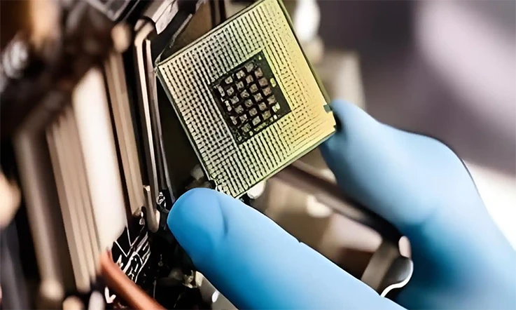
As component density increases and device profiles shrink, integration and assembly techniques must support tighter tolerances, complex mechanical constraints, and diverse interconnect technologies. IC substrates and HDI PCBs now support a wide range of assembly strategies—including flip-chip packaging, system-in-package (SiP) configurations, and embedded passive integration. Each approach brings distinct design, material, and thermal challenges. This section reviews integration flows and design considerations that support assembly reliability and process compatibility across packaging platforms.
IC Substrate Integration in Flip Chip and SiP Modules
IC substrates form the interconnect bridge between silicon dies and printed circuit boards, especially in flip-chip and SiP designs. These applications often demand advanced routing densities, precise pad geometries, and support for heterogeneous die placement.
●Flip Chip Packaging: Flip-chip die attach requires under-bump metallization (UBM) patterns on the die and matching capture pads on the substrate. Common substrate pad pitches range from 130 μm down to 40 μm, depending on redistribution layer (RDL) constraints and bump co-planarity.
●System-in-Package (SiP): Substrates used in SiP must support multiple dies, passive components, and in some cases, stacked memory or RF modules. Routing complexity increases significantly, necessitating use of build-up layers with staggered microvias and laser-drilled interconnects. For example, ABF substrates are frequently used for 3-layer SiP designs to maintain dielectric performance during reflow.
●Assembly Challenges: Delamination during reflow, pad pull-out, or misregistration in bump alignment often lead to yield loss. JEDEC J-STD-033 guidelines are typically used to manage moisture sensitivity in these assemblies.
SMT and Embedded Components in HDI PCBs
Surface-mount technology (SMT) assembly on HDI PCBs involves tighter spacing, smaller component footprints, and integration of active/passive devices directly into the inner layers.
●Component Density: Standard HDI board layouts often place 0201, 01005, or even smaller footprint passives on the top and bottom surfaces. Laser-defined pad registration ensures placement precision during pick-and-place assembly.
●Embedded Components: Resistors and capacitors can be embedded between layers using thin-film or paste-based deposition. This frees surface space while minimizing parasitics. For instance, embedded capacitors under BGA footprints reduce decoupling loop inductance in DDR and high-speed serial buses.
●Solder Joint Reliability: Reflow profiles must be tuned to minimize voids and prevent head-in-pillow (HiP) defects, especially on BGA or PoP assemblies. Solder paste inspection (SPI) and X-ray verification are applied post-reflow to confirm joint integrity.
Using embedded technology in HDI design improves routing flexibility while also shrinking the form factor. But attention must be paid to the z-axis stack tolerances and thermal expansion mismatch during reflow.
Design for Assembly: Warpage Mitigation and Co-planarity
Design for assembly (DFA) practices help reduce production variability, especially during die bonding, reflow soldering, or multilayer lamination. Warpage and co-planarity issues often arise when using thin dielectric build-up, high-Tg resin systems, or dense via structures.
●Warpage Control: Warpage often occurs during reflow or thermal cycling. For IC substrates, material selection (e.g., low CTE core with ABF buildup) is used to reduce stress-induced curvature. Process adjustments—such as symmetrical layer stackups or balanced copper distribution—further help maintain flatness.
●Co-planarity Constraints: Co-planarity between capture pads, solder lands, or embedded component connections must remain within 20–40 μm for reliable bonding. Non-coplanar surfaces lead to poor solder wetting or incomplete assembly. Optical metrology tools such as white light interferometers are used for surface flatness validation before assembly.
Example: A typical flip-chip IC substrate with an ABF build-up layer and 12-layer structure may experience 40–60 μm warpage post-reflow if copper balance isn’t addressed. Yield losses can exceed 5% if planarity targets are not met.
Trends in Miniaturization and Advanced Packaging
Advancements in semiconductor packaging and HDI PCB fabrication are driven by the need for increased integration density, improved performance, and cost-effective manufacturing. This section delves into the evolution of IC substrates, the development of HDI PCB fabrication techniques, and the challenges associated with integration density and interconnect routing.
IC Substrate Evolution: Fan-Out, Embedded Bridge, and 2.5D/3D ICs
The progression of IC substrate technologies has introduced various packaging solutions aimed at enhancing performance while managing cost and lead time.
●Fan-Out Wafer-Level Packaging (FOWLP): FOWLP eliminates the need for an interposer, which helps lower material usage and supports thinner package profiles. This method aligns with the requirements of mobile and IoT applications where space constraints and cost targets are tightly managed.
●Embedded Bridge Technologies: Techniques like Intel’s Embedded Multi-die Interconnect Bridge (EMIB) integrate a silicon bridge within the substrate, facilitating high-density interconnects without the full cost of a silicon interposer. This method offers a balance between performance and cost.
●2.5D and 3D Packaging: 2.5D packaging utilizes an interposer to connect multiple dies side by side, while 3D packaging stacks dies vertically. While these approaches offer significant performance benefits, they also introduce complexities in thermal management and manufacturing, potentially impacting lead times and costs.
Table 1: Comparison of Advanced Packaging Techniques
| Packaging Type | Cost Implications | Lead Time Considerations | Application Areas |
| FOWLP | Lower | Shorter | Mobile, IoT |
| Embedded Bridge | Moderate | Moderate | High-performance computing |
| 2.5D/3D | Higher | Longer | Data centers, AI |
HDI PCB Development: mSAP, aSAP, and Ultra-Fine Line Fabrication
The evolution of HDI PCB fabrication techniques focuses on achieving finer line widths and spaces to accommodate increased circuit density.
●Modified Semi-Additive Process (mSAP): mSAP allows for the creation of ultra-fine lines and spaces, enhancing routing density. This method is widely adopted in smartphone manufacturing due to its balance between performance and cost.
●Advanced Semi-Additive Process (aSAP): aSAP further refines the capabilities of mSAP, enabling even finer features. While offering superior performance, aSAP may involve higher manufacturing costs and longer lead times due to increased process complexity.
●Ultra-Fine Line Fabrication: Techniques achieving line widths below 10 µm are being explored to meet the demands of high-speed and high-frequency applications. These methods require advanced equipment and stringent process controls, impacting both cost and lead time.
Table 2: HDI PCB Fabrication Techniques
| Technique | Minimum Line Width | Cost Impact | Lead Time Impact | Typical Applications |
| mSAP | ~30 µm | Moderate | Moderate | Smartphones, tablets |
| aSAP | <20 µm | Higher | Longer | High-speed computing |
| Ultra-Fine | <10 µm | Highest | Longest | RF modules, HPC |
Integration Density and Interconnect Routing Limits
As integration density increases, challenges in interconnect routing become more pronounced, affecting both manufacturing complexity and cost.
●Routing Challenges: Higher integration density necessitates narrower traces and smaller vias, increasing the complexity of the PCB design and fabrication processes. This can lead to higher rejection rates and longer manufacturing times.
●Thermal Management: Densely packed circuits generate more heat, requiring advanced thermal management solutions. Implementing these solutions can add to the overall cost and complexity of the product.
●Signal Integrity: Maintaining signal integrity becomes more challenging with increased integration density, necessitating careful design and potentially more expensive materials or processes.
Table 3: Impact of Integration Density on Manufacturing
| Factor | Impact on Cost | Impact on Lead Time | Mitigation Strategies |
| Routing Complexity | Increased | Extended | Advanced design tools |
| Thermal Management | Increased | Extended | Enhanced cooling solutions |
| Signal Integrity | Increased | Extended | High-quality materials |

