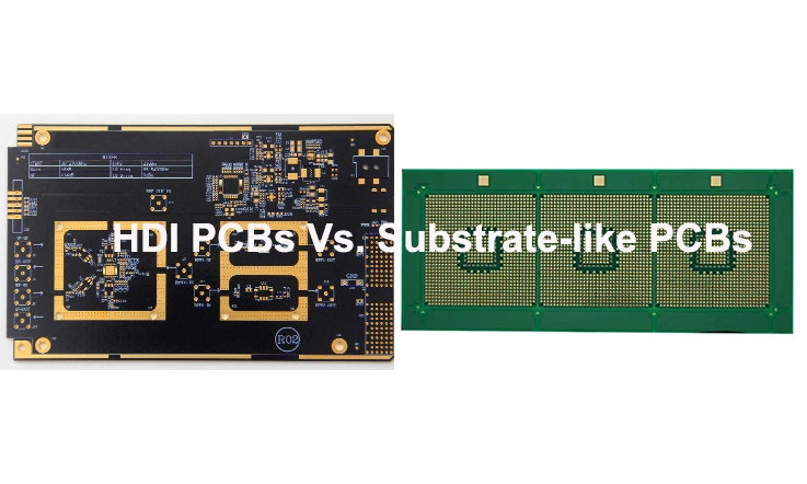
In the continuously advancing domain of electronics, the need for sophisticated printed circuit board has been escalating. Two notable players in this field are High Density Interconnect (HDI) PCB and Substrate like PCB. While each serves unique functions, it is vital to comprehend their distinctions and uses. This discourse offers an exhaustive comparison between HDI PCB and Substrate like PCB, illuminating their distinctive feature, application, and importance in the sphere of contemporary electronics.
Background on PCB
Printed circuit boards are integral components in modern electronics, providing a structured and dependable platform for interconnecting electronic elements and facilitating signal transmission. PCB are constructed using a non-conductive substrate material, commonly fiberglass or a composite material, upon which conductive copper traces are patterned.
Historical Development of PCB:
●Early 1900s: The inception of the first printed circuit board took place, featuring copper foil on an insulating substrate.
●1940s: PCB gained traction in military and industrial domains due to their reduced size and augmented reliability.
●1950s: The introduction of double side PCB with plated through holes for interconnections occurred.
●1960s and 1970s: PCB fabrication techniques progressed, encompassing the advent of multi-layer PCB and surface mount technology.
Types of PCB:
●Single sided PCB: These consist of single layer of copper traces on one side of the substrate.
●Double sided PCB: Copper traces exist on both facets of PCB base substrate, interconnected by plated through holes.
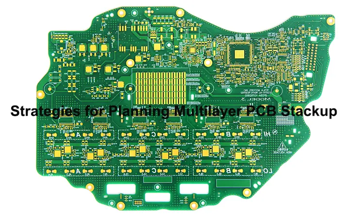
●Multi layer PCB: These exhibit multiple tiers of copper traces, separated by insulating layers and interconnected by vias.
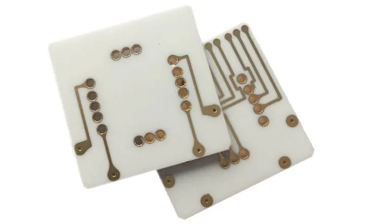
●Rigid PCB: Use rigid substrate materials made, like fiberglass or composites.
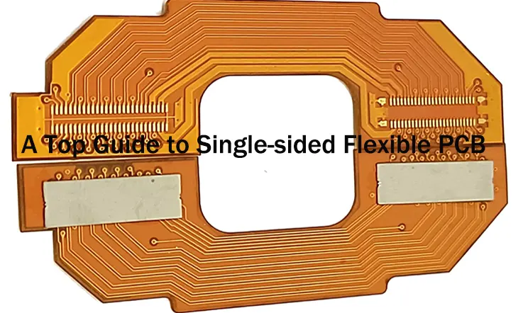
●Flexible PCB: Use flexible substrate materials manufacturing, facilitating bending and flexing.
Applications of PCB:
PCB find application in a diverse range of electronic devices, including:
●Computers and laptops
●Smartphones and tablets
●Industrial control systems
●Medical equipment
●Aerospace and defense systems
●Consumer electronics
Advantages of PCB:
●Compact size and high density
●Enhanced reliability and durability
●Reduced assembly time and cost
●Improved signal integrity and performance
Future Trends in PCB:
●Continued miniaturization and increased density
●Integration of advanced materials and technologies
●Flexible and conformable PCB
●Advanced manufacturing techniques, such as additive manufacturing
Distinction between HDI PCB and Substrate-like PCB
Distinguishing between HDI PCB and substrate-like PCB is vital given their unique attributes and appropriateness for diverse applications. Grasping these variances is key for refining designs, evaluating manufacturing capacities, overseeing expenses and delivery times, and guaranteeing performance and dependability.
Design Considerations: comprehension of HDI PCB and substrate-like PCB empowers designers to customize their designs to effectively accommodate specific application requirements effectively.
Manufacturing consider: HDI PCB and substrate-like PCB demand distinct manufacturing technology. Hence, contemplating the professional of the manufacturer becomes paramount when selecting the suitable PCB type.
Cost and Lead Time Considerations: The intricacies and specific manufacturing methodologies pertinent to each type of PCB significantly influence their associated costs and production lead times. Evaluating these factors helps in making informed decisions regarding budget and project timelines.
Performance and Reliability: The selection between HDI PCB and substrate-like PCB can significantly influence the overall performance and reliability of electronic devices. Choosing the right PCB type ensures optimal functionality and durability.
Definitions and Characteristics
High Density Interconnect PCB:
Definition: HDI PCB are printed circuit boards designed with a high density of interconnections, achieved through the utilization of advanced via technologies such as microvias, blind vias and buried vias.
Characteristics:
1. Fine line widths and spacing, usually less than 100 microns.
2. Multiple layers, often exceeding 10 layers.
3. Implementation of advanced via technologies, including microvias, blind vias and buried vias.
4. Complex and dense routing patterns to accommodate high interconnect density.
5. Miniaturized components and high component density.
Substrate-like PCB:
Definition: Substrate-like PCB are printed circuit boards that share similarities with rigid-flex PCB in appearance and functionality, but employ a different manufacturing process. These PCB offer a high degree of flexibility and durability.
Characteristics:
1. Flexible substrate material, typically made of polyimide.
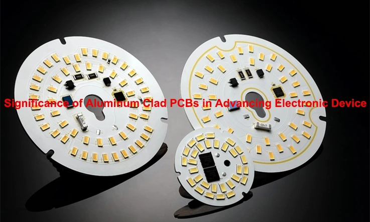
2. Incorporation of rigid reinforcement layers, commonly using FR4 or aluminum.
3. Interconnections facilitated through plated-through holes or conductive vias.
4. High-density routing and component placement to maximize functionality.
5. Excellent electrical and thermal properties.
Comparison of HDI PCBs and Substrate-like PCBs:
| Feature | HDI PCBs | Substrate-like PCBs |
| Substrate material | Rigid (fiberglass or composite) | Flexible (polyimide) |
| Interconnections | Microvias, blind vias, buried vias | Plated-through holes, conductive vias |
| Density | Very high | High |
| Flexibility | Limited | High |
| Applications | High-speed digital circuits, mobile devices | Wearable devices, foldable displays |
Key Differences:
1.HDI PCB focus on achieving high interconnect density and miniaturization, while substrate-like PCB prioritize flexibility and durability.
2. HDI PCB employ advanced via technologies such as microvias, blind vias and buried vias, whereas substrate-like PCB typically use plated-through holes or conductive vias.
3. HDI PCB exhibit more rigidity, while substrate-like PCB offer greater flexibility.
Manufacturing Processes
High Density Interconnect PCB:
Layer Fabrication:
●Begin with a rigid substrate material, like fiberglass or composite material.
●Apply thin layer of copper foil to the substrate.
●Utilize photolithography and etching processes to pattern the copper traces.
Via Formation:
1. Drill or laser microvias, blind and buried vias into the substrate.
2. Plate the vias with copper to establish conductive interconnections.
Lamination and Pressing:
1. Laminate the layers together using a high temperature press.
2. Apply heat and pressure to bond the layers and cure the adhesive.
Substrate-like PCB:
Substrate Preparation:
1. Commence with a flexible substrate material, like polyimide.
2. Apply thin layer of copper foil to the substrate.
3. Employ photolithography and etching processes to pattern the copper traces.
Reinforcement Layer:
1. Apply layer of rigid material, like FR4 or aluminum, to one or both sides of the substrate.
2. Bond the reinforcement layer to the substrate using an adhesive
Via Formation:
1. Drill or laser plated-through holes or conductive vias into the substrate and reinforcement layers.
2. Plate the vias with copper to establish conductive interconnections.
Lamination and Pressing:
1. Laminate the layers together using a high temperature press.
2. Apply heat and pressure to bond the layers and cure the adhesive.
Comparison of Manufacturing Processes:
| Process Step | HDI PCBs | Substrate-like PCBs |
| Substrate material | Rigid (fiberglass or composite) | Flexible (polyimide) |
| Via formation | Microvias, blind vias, buried vias | Plated-through holes, conductive vias |
| Reinforcement layer | Not applicable | Optional |
| Lamination and pressing | Multi-step process | Single-step process |
Key Differences:
1. HDI PCB involve more intricate and precise manufacturing processes to accommodate the high density of interconnections and advanced via technologies.
2. Substrate-like PCB employ a simpler manufacturing process, with the notable addition of a reinforcement layer for enhanced flexibility and durability.
Applications
High Density Interconnect PCB:
Applications:
●High speed digital circuits
●Mobile device
●Laptops and notebooks
●Gaming consoles
●Automotive electronics
●Medical device
●Aerospace and defense application
Substrate-like PCB:
Applications:
●Wearable devices
●Foldable displays
●Medical implants
●Industrial automation
●Automotive electronics
●Robotics
Comparison of Applications:
| Application | HDI PCBs | Substrate-like PCBs |
| High-speed circuits | Yes | No |
| Mobile devices | Yes | Yes |
| Wearable devices | No | Yes |
| Foldable displays | No | Yes |
| Medical implants | No | Yes |
| Industrial automation | Yes | Yes |
Key Differences:
●HDI PCB are extensively used in the latest smartphones to achieve high performance and a compact size, enabling advanced features and functionalities.
●Substrate like PCB are utilized in wearable device like smartwatches and fitness trackers, offering adaptability and comfortable usability.
●HDI PCB are deployed in automotive electronics, encompassing ADAS systems, to satisfy the stringent prerequisites of dependable and high speed velocity signal transmission.
●Substrate-like PCB are employed in medical implants to furnish robust and dependable connections in compact and intricate devices, guaranteeing patient safety and efficient operation.
Industry Trends and Future Outlook
Growing Demand for HDI PCB:
The escalating trend of miniaturization and complexity in electronic devices is propelling the need for HDI PCB. These PCB provide multiple advantages, include increased packaging density, enhanced signal integrity, and diminished power usage. As electronic devices evolve to become more compact and sophisticated, HDI PCB are vital in fulfilling the requirements for streamlined design and high performance functionality. Moreover, the expansion of emerging technologies like 5G, artificial intelligenceand the Internet of Things, it is further boosting the demand for HDI PCB, as these technologies necessitate the integration of intricate circuitry and high speed signal transmission.
Evolution of Substrate like PCB:
Substrate like PCB are witnessing a rise in demand due to the growing need for flexible and wearable electronics. Progress in materials and fabrication methods have led to the creation of substrate like PCB with improved flexibility, resilience and overall performance. These PCB are very suite for application demanding adaptability and resistance to environmental elements. Furthermore, the incorporation of sophisticated sensing and communication technologies into substrate like PCB is broadening their application range, paving the way for innovative solutions in fields like wearable devices, medical implants, industrial automation and robotics.
Technological Advancements and Future Applications:
The future of PCB manufacturing is being shaped by advancements bringing new opportunities. 3D printing, also referred to as manufacturing is changing how PCB are made by allowing for complex and customized designs. This innovation offers increased flexibility in design and faster prototyping resulting in launches of electronic products. Furthermore the development of materials, with improved electrical, thermal and mechanical properties is pushing the boundaries of PCB performance enabling higher speeds and reliability. The rise of stretchable PCB is transforming the world of adaptable electronics making way for wearable health monitors, soft robotics and other applications that require flexible circuitry.
Future Outlook:
HDI PCB and substrate like PCB will persistently maintain a crucial role in the progression of electronics. As the demand for more compact, intelligent and interconnected devices intensifies, the requirement for high performance PCB will endure. Furthermore, the merging of HDI and substrate like technologies could potentially result in the creation of new hybrid PCB types that offer distinctive capabilities, amalgamating the benefits of both methodologies. The industry can anticipate continual innovation in PCB manufacturing, material, and designs to accommodate the evolving need of various sectors, encompassing consumer electronics, automotive, aerospace, medical and industrial application. Overall the future looks promising for HDI PCB and substrate like PCB as drivers of technological progress in the electronics industry.
In a Word
The difference between HDI PCB and substrate like PCB lies in their characteristics and intended uses. HDI PCB are known for their efficiency in speed digital circuits and compact size making them popular for mobile devices, laptops, gaming consoles and automotive electronics. Conversely substrate like PCB are valued for their flexibility, durability and ability to withstand conditions making them ideal, for wearable devices, foldable displays, medical implants and industrial automation systems.
With the escalating demand for more compact, intelligent, and interconnected electronic devices, the importance of both HDI PCB and substrate like PCB in driving technological progress is paramount. By comprehending their unique capabilities and applications, manufacturers and designers can harness these PCB technologies to cater to the dynamic needs of consumers across diverse sectors.

