
In the field of electronic and electromechanical components, electrical contacts are fundamental in facilitating interconnections between individual points. The schematic diagram of an electronic device maps out the necessary interconnection pattern that is required to achieve the intended functionality.
While the printed circuit board is essential to electronic products, it alone does not constitute a complete product. Therefore, there is a need for external connections, including those between PCB, PCB and components, or PCB and product panels. Therefore select an interconnection method that balances reliability, ease of manufacturing and cost is a vital consideration in PCB design. Since various interconnection method have feature it is important to select the method that suits the particular needs of each design carefully.
What is interconnect PCB?
Interconnect PCB is specifically designed to enable connections between multiple electronic components or devices on a single board. It includes a conductive pattern of tracks, pads, and vias that interconnect various components and connect them to other circuits or power sources. The Interconnect PCB is commonly used in a range of electronic applications from everyday consumer electronics to advanced industrial machinery, where reliable and effective connections are key, for the devices overall performance and functionality.
What Benefits Do Interconnect PCB?
A reliable interconnect PCB is essential for the optimal functioning of electronic device, as it directly influences the electrical performance, mechanical stability and long term durability of the entire system.
Benefits:
● Improved Electrical Performance
● Enhanced Mechanical Stability
● Reduced Manufacturing Costs
● Easy Troubleshooting and Maintenance
● Better Product Quality and Customer Satisfaction
Guidelines for Interconnect PCB Design and Manufacture
Design and manufacturing guidelines are essential to ensure that interconnect PCB are reliable, efficient, and meet the desired performance specifications.
The Guidelines Step:
1 PCB Stackup and Layer Count
The PCB stack-up should be engineered to minimize signal interference and maintain signal integrity. The layer count should be optimized to offer adequate routing capacity while avoiding excessive complexity and cost.
2 Routing and Trace Width Considerations
When routing traces, it is crucial to minimize signal path lengths to mitigate crosstalk and interference from other signals, such as power and ground. Selecting appropriate trace widths is essential to guarantee sufficient current carrying capacity, considering both space limitations and manufacturability.
3 Component Placement and Orientation
Optimizing component placement is crucial to minimize routing distances and prevent signal interference. The orientation of components should be chosen to align with the preferred manufacturing process and to ensure easy accessibility for inspection and maintenance.
4 Manufacturing Tolerances and Process Capability
The selection of design tolerances should align with the capabilities of the manufacturing process to guarantee effective, dependable, and consistent manufacturing. It is essential to utilize a suitable PCB design for manufacturability (DFM) methodology to minimize fabrication challenges and lower costs.
5 Testing and Reliability Considerations
The PCB design should undergo thorough testing for both electrical and mechanical integrity, with a well structured testing strategy to ensure reliability. The design and layout should incorporate reliability enhancing techniques, including proper ESD protection, thermal management and mechanical strain relief.
By following these guidelines a interconnected PCB can be. Produced and design to meet the necessary electrical and mechanical performance requirements guaranteeing smooth and dependable functioning of the electronic system.
Printed Circuit Board Interconnection Method
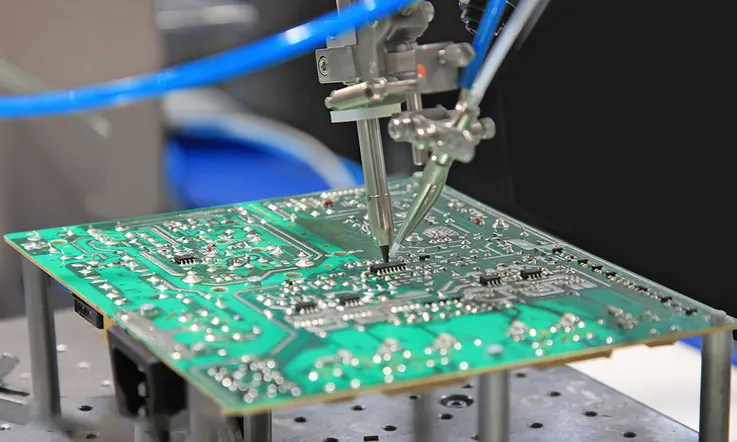
Welding Method
The connection method boasts simplicity, low-cost implementation, high reliability, and circumvents failures that may result from poor contact. However, it also presents certain drawbacks, including limited convenience for interchangeability or maintenance. This method is commonly adopted when there are fewer external leads associated with the component under consideration.
● PCB Wire Welding: This method omits the need for any connectors, as external connection points on the PCB printed board are directly soldered to the components or other components outside the board via wires. Examples of scenarios where this method applies include a speaker in a radio or a battery case.
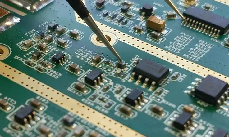
In the soldering process, it is crucial to focus on the interconnection of the board. Position the soldered wire pads as close to the edge of the PCB printed board as feasible and ensure uniformly sized to simplify soldering and maintenance.
Holes should be drilled near the solder joint on the PCB printed board to improve the wire connection’s mechanical strength and prevent the wire or printed wire from becoming detached due to pulling. Through these via holes, the wire should be passed from the surface of the component through the pad hole for soldering.
Neatly arrange or bundle the wires and secure them with wire cards or other fasteners to prevent movement-induced wire breakage.
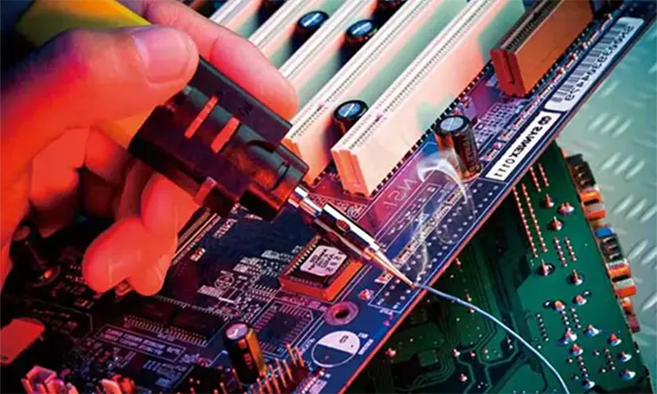
● PCB Cable Welding: When two PCB printed boards require a connection, a cable junction is often used due to its reliability, but it can be challenging to establish a connection. This method does not limit the relative positions of the two PCB boards.
Another alternative is direct soldering between the PCB printed boards, which is frequently implemented when the boards are oriented at a 90-degree angle. Once joined, the resulting product comprises a single, unified PCB printed board component.
Connector Connection Method
In the case of more complex instruments and equipment, connector-based interconnection is a prevalent method. This “building block” structure ensures the quality of the products manufactured en masse, reduces system costs, and fosters convenience when debugging and conducting maintenance.
When equipment malfunctions, maintenance staff does not need to conduct component-level inspections to trace the source of the issue, ascertaining the failed board is enough to replace it promptly. This approach allows for rapid troubleshooting, reducing downtime and bolstering equipment utilization. The replaced circuit board can be repaired at leisure and used as a spare part once it has been fixed.
● Printed Circuit Board Socket: In complex instruments, an interconnection type that is often used is the printed plug connection. In this method, the plug is produced from the edge of the printed circuit board (PCB) and is designed based on the socket’s size, number of contacts, contact distance, positioning hole location, and other specific requirements necessary to match the customized PCB socket.
During plug fabrication, the plug part undergoes gold plating to enhance wear resistance and reduce contact resistance. This approach is simple to assemble, easily interchangeable, has good maintenance performance, and is suitable for standardized mass production. The disadvantage is that the PCB’s manufacturing cost is elevated, and there are high precision and process requirements associated with printed board manufacturing. This method’s reliability is slightly compromised since the plug portion can oxidize or the socket spring can deteriorate, leading to poor contact. To bolster external connection reliability, cords with equal lead wire taken in parallel pass through same-side or two-side circuit board contacts.
A PCB printed circuit board socket connection method is often chosen for multi-board structure products, featuring two types of reed and pin-type sockets for integration with a socket or the PCB or base plate.
● Standard Pin Connection: This approach is applicable for external connections in printed boards, particularly in small instruments. The method involves integrating the two printed boards through standard pins, which can be either perpendicular or parallel, thereby simplifying mass production.
Considerations for Selecting Interconnect PCB Method
● Electrical Performance: The choice of interconnect PCB method should align with the necessary electrical performance criteria, encompassing signal integrity, power distribution, thermal management, and more. This involves the selection of suitable materials, trace dimensions, spacing, impedance control, and other essential electrical parameters.
● Mechanical Stability: The interconnect PCB method should provide the necessary mechanical stability to support the components and withstand the stresses of temperature variations, vibration, shock and other environmental factors. This includes selecting the appropriate thickness, layer count and stacking configuration, as well as the use of stiffeners, adhesives and other support structures.
● Manufacturing Tolerance and Cost: When select on the interconnect PCB method, it is vital to consider the necessary manufacturing tolerances and capabilities, alongside the overall cost and lead time constraints. This encompasses the selection of the right manufacturing process, material availability, and panel utilization to meet the specified requirements.
● Design Complexity: When choosing the interconnect PCB method, it is crucial to consider the design complexity requirements, including the number of layers, component density, interconnect type, and circuit intricacy. This entails choosing suitable manufacturing capabilities and equipment, along with designing for manufacturability.
● Volume and Lead Time: In choosing the interconnect PCB method, it is essential to consider the production volume and lead time specifications, taking into account factors such as raw material availability, equipment capacity, and production efficiency. This ensures alignment with the required manufacturing demands and timelines.
By considering these factors, and working with a trusted interconnect PCB provider, it is possible to select the most appropriate method to achieve the desired electrical.
Designing for Effective High-Speed Interconnection
For high speed design interconnectivity, especially for clock signals and triggers in communication interfaces, specific considerations are necessary to ensure optimal system performance, particularly in low-power environments. It is vital to minimize cross talk and excess noise generation among other factors.
Impedance matching is a necessary aspect of high speed design since it maximizes power transfer and minimizes signal reflection. At high speeds, a signal from a low impedance source transferring to a high impedance destination will flip its phase 180 degrees back and forth without proper termination at each end.
When dealing with high speed SPI communication, it is prudent for designers to contemplate integrating in-line resistors or buffers prior to linking with an external board. The selection of resistance should be commensurate with the PCB trace impedance, as too little resistance can result in excessive current consumption, while using too much will have little impact on improving signal transfer.
In high speed signal design, it is advisable to incorporate a ground connection between alternate pins on the connector. By arranging the ground pins around those handling power and signals, for instance, (pin 1 = power, pin 3 = trigger 1, pin 5 = trigger 2, pin 7 = trigger 3, and pins 2, 4, 6, and 8 are all ground). This method helps reduce inductive coupling and cross talk.
These tried and true tips and considerations contribute to effective interconnectivity of PCB. Designers should, from the outset, analyze the product objectives and market demands, leveraging advanced design software to progress through a comprehensive workflow that encompasses critical design, testing, manufacturing, and servicing elements, all before commencing the initial board fabrication.
Why It’s Important to Define the Appropriate Components?
There are numerous options available when researching components needed for circuit board assembly, as defined by the design. Although the internet is an excellent source of information, trying to sift through marketing jargon can be challenging.
Meeting with manufacturer representatives is an alternative approach to learn about the latest technologies; however, there is the potential for this interaction to be purely sales-driven. Nonetheless, certain manufacturers may be willing to share their expertise, offer insight into industry standards, share past experiences, and provide samples, resulting in them serving as a valuable resource.
Future Outlook for Interconnect PCB Technology
The trajectory of interconnect PCB technology moving forward is propelled by the escalating need for enhanced performance, functionality and miniaturization in electronic device. Several emerging trends and advancements are poised to influence the evolution of interconnect PCB technology in the foreseeable future.
● High Speed and Low Loss Interconnects: The increasing need for heightened data rates and reduced signal losses is propelling the evolution of sophisticated interconnect technologies, encompassing low-loss dielectric materials, signal integrity optimized routing and integrated passive components.
● Advanced Manufacturing Processes: The incorporation of sophisticated manufacturing techniques like 3D printing, additive manufacturing, and laser direct imaging is empowering the fabrication of increasingly intricate and compact interconnect PCB, simultaneously driving cost efficiencies and expediting lead times.
● Flexible and Stretchable Circuits: The advancement in flexible and stretchable interconnect PCB is facilitating the emergence of innovative applications in areas such as wearable and implantable electronics, soft robotics and biomedical device.
● High Density Integration: The requirement for miniaturization and greater component densities is steering the progress of cutting edge stacking and interposer technologies, facilitating the incorporation of multiple layers of components within a singular interconnect PCB.
● Material Developments: Advancements in materials, including the utilization of emerging substances like graphene, nanotubes and other nanomaterials, are poised to drive the innovation of cutting edge interconnect PCB technologies characterized by enhanced electrical performance, superior thermal dissipation and heightened reliability.
Final Thoughts
Interconnect PCB technology plays a vital role in the functioning and performance of electronic device. The choice of the suitable interconnect PCB method is contingent on various factors, such as the necessary electrical and mechanical performance standards, design intricacy, manufacturing tolerances and costs, as well as volume and lead time demands. This comprehensive consideration ensures optimal selection for the intended application.
The Commonly interconnect PCB methods, comprising surface mount technology, through-hole technology, multi-chip modules, and flexible and rigid-flex PCB, each carry inherent advantages and limitations. Through diligent evaluation of these factors and collaboration with a reputable interconnect PCB provider, one can judiciously determine the most suitable method that meets the desired electrical and mechanical performance criteria while effectively addressing cost considerations and lead time constraints.
JarnisTech, situated in China, stands as a distinguished PCB manufacturing and assembly facility providing a complete spectrum of Turnkey PCB assembly services encompassing component procurement to PCB assembly. Should you have a forthcoming PCB project necessitating our expertise, we welcome your prompt engagement with us without any reservations.