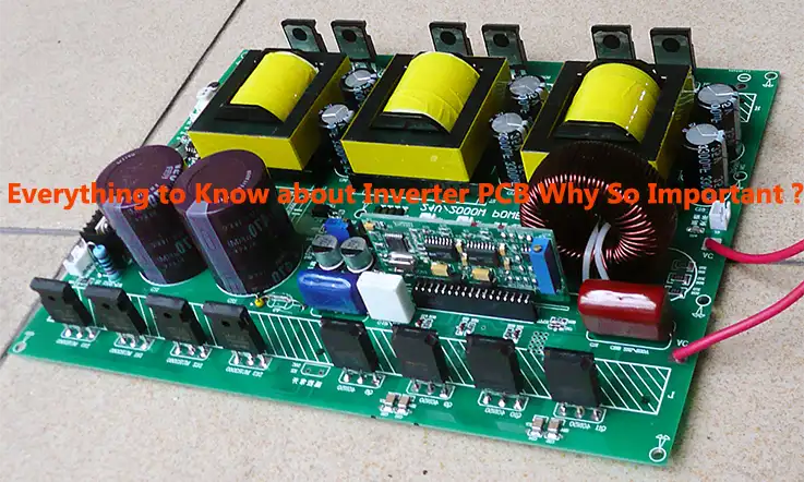
The design and manufacturing of Inverter PCBs require high precision and attention to detail in order to ensure efficient and reliable operation. Inverter PCBs must also be able to handle high loads and operate over extended periods without overheating or failing, which underscores their importance in a wide range of applications.
For those seeking comprehensive knowledge on inverter printed circuit boards (PCBs), this guide offers detailed information on topics including PCB design, material selection, classification, features, applicable standards, specifications, and fabrication processes. Whether you are looking to expand your expertise in this domain or seeking answers to specific questions about inverter PCBs, this guide provides a valuable resource for any PCB engineer.
Why are Inverter PCBs Important ?
Inverter PCBs are important for several reasons:
● AC Power Conversion: Inverter PCBs are designed to convert DC power into AC power, which is necessary for operating many appliances and devices that require AC power.
● Energy Efficiency: Inverter PCBs enable greater energy efficiency by converting DC power into AC power with greater precision and control, reducing energy consumption and improving overall performance.
● Cost Savings: Inverter PCBs can lead to cost savings through increased energy efficiency and reduced maintenance costs.
● Reliability: Inverter PCBs are designed to operate over extended periods without failure, providing reliable power conversion for a wide range of applications.
● Renewable Energy: Inverter PCBs play a critical role in renewable energy systems, such as solar and wind power systems, by converting DC power produced by the solar panels or wind turbines into AC power that can be used for homes and businesses.
Overall, Inverter PCBs are important because they enable the efficient and reliable conversion of DC to AC power, which is essential for many appliances and devices. Their use can result in energy savings, cost savings, and improved reliability, making them a critical component in a wide range of applications.
What is Inverter PCB ?
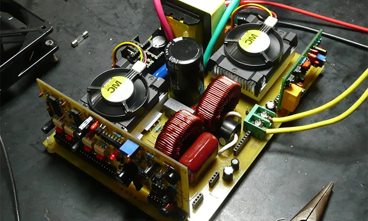
An inverter PCB is a printed circuit board utilized within equipment that converts direct current (DC) electrical energy, typically from a battery or accumulator jar, into alternating current (AC) at a nominal output voltage of 220 volts and a frequency of 50Hz sinusoidal waveform. The composition of this inverter typically includes an inverter bridge, control logic, and filter circuit. Inverters are commonly found in household appliances such as air conditioners, home theaters, electric grinding wheels, sewing machines, DVDs, VCDs, computers, televisions, washing machines, smoke lampblack machines, refrigerators, video recorders, massagers, electric fans and lighting.
Due to the increasing prevalence of automobiles, individuals who travel or commute frequently may also use an inverter to power various electrical appliances and tools using an onboard battery. Inverters for use in vehicles are commonly available in power specifications of 20 W, 40 W, 80 W, 120 W, and 150 W, typically designed to be powered via the vehicle’s cigarette lighter socket. For higher power output inverters, a connection to the vehicle’s battery is required. By connecting the inverter output to household electrical appliances as mentioned earlier, it is possible to use these devices while traveling in an automobile.
Which Material is Used to Manufacture an Inverter PCB ?
The selection of materials for manufacturing inverter PCBs is dependent upon the specific requirements of the application. While various materials can be used to fabricate inverter PCBs, copper is one of the most commonly employed primary materials. This is mainly attributed to its high electrical conductivity, which allows for efficient transmission of electrical energy and signals without disruption. In addition to copper, other materials may be used in the production of inverter PCBs, depending on the specific needs of the application:
● Plastic
● Aluminum
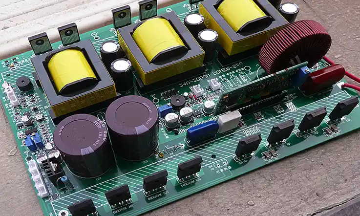
Types of Inverter Printed Circuit Boards
Inverter PCBs are available in three main types, offering a range of options for individuals seeking to select the appropriate circuit board for their application needs. These types can be classified based on their design, layout, and specific features to suit different requirements.
● Single Sided Inverter PCB: Single-layer (or single-sided) inverter PCBs are designed with just one layer of material or base substrate, featuring a single copper coating layer on one side followed by a silkscreen or solder mask. All necessary components are positioned on one side of the board, making circuit design and manufacturing a more straightforward process. Single-layer inverter PCBs are a cost-effective and user-friendly option, particularly suitable for applications with simpler circuit designs.
● Double Sided Inverter PCB: Double-layer (or double-sided) inverter PCBs feature copper metals on both sides of their base plates, with holes connecting the circuits from one side to the other. These PCBs may utilize through-hole or surface-mounting technology for component connection. Double-layer inverter PCBs are ideal for applications of moderate complexity, such as power supplies.
● Multilayer Inverter PCB: Multilayer inverter PCBs are designed with at least three double-sided inverter PCBs placed in alignment and secured together using a specialized type of glue. These PCBs also feature various insulation materials placed between the boards to provide additional protection against heat damage.
Multilayer inverter PCBs are an excellent choice for complex electrical applications such as GPS technology and file servers due to their advanced design and technical capabilities. By utilizing these PCBs, individuals can achieve optimal electrical performance while maintaining maximum thermal stability and protection.
Benefits of Using Inverter PCB
Inverter PCBs are widely recognized as a vital component utilized in modern electronic equipment. These circuit boards enable connections between various passive and active components, offering a range of benefits such as optimal electrical performance and efficient circuit design. Inverter PCBs have become an essential element of many electronic devices, contributing to their functionality, reliability, and longevity.
● Saves wire via its compact size: The use of copper tracks on inverter printed circuit boards provides a space-saving solution by replacing the need for bulky wire types. Wires may take up a considerable amount of space on a circuit board, potentially leading to an increase in size. However, the compact nature of copper tracks allows for a more efficient use of space, resulting in smaller and more streamlined inverter PCB designs. This promotes overall device miniaturization and enables the development of smaller, more portable electronic products.
● Diagnosing and Repairing is Easy: In the event of a malfunction with an inverter PCB, identifying the source of the problem is a relatively straightforward process. This can save time and resources that would otherwise be required to diagnose or troubleshoot the issue. Additionally, replacing faulty parts of the inverter PCB is a cost-effective solution that does not require extensive personnel or material resources. This ensures that repairs can be made efficiently, minimizing any potential disruptions or downtime for the device or system.
● Saves Time: Assembling the parts of an inverter PCB is an efficient process that can save a significant amount of time. The use of advanced machinery and technology in connecting the circuit components offers a cost-effective solution compared to traditional assembly methods, reducing labor costs and saving time for other tasks or projects. By utilizing modern PCB assembly techniques, the inverter PCBs can be produced efficiently without compromising on quality or durability.
● Prevents Frequent Movement: Inverter PCB components are securely mounted onto the board, limiting the possibility of movement and potential damage. This ensures stability and reliability, making it easier to handle and transport devices without compromising their integrity.
● Low Noise: Inverter PCBs are recognized for their capacity to operate silently, producing minimal electronic noise. With proper connections and installation, these circuit boards are capable of reducing the level of electronic noise generated in a system, resulting in improved overall performance and reduced interference.
What are the Limitations of the Inverter PCB ?
Although the inverter PCB offers several advantages, there are also several limitations associated with their use. Here are some of the drawbacks to consider when utilizing inverter PCB technology.
● Requires Concrete Layout Efforts: Designing an inverter PCB requires careful attention to detail, particularly in laying out the entire circuit. This is a crucial step in ensuring that the PCB functions optimally and meets the required performance standards. Given the complexity of many inverter PCB designs and the presence of sensitive components, a high degree of vigilance and skill is necessary to ensure that the layout is accurate and error-free. This process may require extra effort and expertise, given that mistakes in the layout can have significant consequences, including causing time delays and potential damage to the circuit itself.
● No Chances of Updates: One of the potential limitations of inverter PCBs is that once printed, the board layout becomes permanent and cannot be easily modified or updated. This permanent nature of the layout makes it crucial to ensure that all necessary design elements are correct before proceeding with the printing process to avoid costly errors and reprints. In situations where updates are required, the only recourse may be to design and print an entirely new PCB. Hence, careful planning and consideration are necessary to ensure that the initial PCB design accurately meets all system requirements.
● High Initial Cost: The upfront costs associated with the planning, design, and development of an inverter PCB can be substantial. As such, it is essential to have a well-defined budget in place that can support the various expenses involved in the PCB creation process. This is particularly important given that the design and development of inverter PCBs typically involve advanced technology, specialized software, and skilled labor. By allocating adequate resources and budget for the project, you can ensure that the product meets the necessary quality standards while also remaining financially viable.
● Environmental Pollution: The manufacturing process of inverter PCBs typically involves etching, which can produce a significant amount of chemical waste that poses environmental pollution risks. This highlights the importance of responsible and sustainable production practices that minimize the harmful impact on the environment. As such, it is essential to follow appropriate health and safety guidelines as well as disposal regulations when working with chemicals during the production process.
How Does an Inverter PCB Work ?
Inverter PCBs are designed to convert direct current (DC) into un-interrupted alternating current (AC), which is a crucial function in many power supply applications. When AC power is present, the inverter PCB senses its presence and allows for charge to flow to the battery charging section. The sensors then activate a relay, which passes the AC mains supply through to the output socket. Using line voltage, the AC is inverted into DC, which charges the battery until sensors detect that it is fully charged.
Some inverter PCBs come equipped with trickle charging circuits that help maintain the battery at full capacity. This feature ensures that the battery is kept in its ideal operational state, prolonging its lifespan and maintaining optimal performance. The overall functionality of an inverter PCB is a highly complex process that requires careful design and engineering to ensure that it can perform reliably and efficiently in real-world conditions.
Troubleshooting Inverter PCBs
Troubleshooting Inverter PCBs typically involves the following steps:
● Identify the Problem: The first step is to identify the specific problem with the Inverter PCB. This can include issues such as component failure, power supply problems, or incorrect wiring.
● Inspect the PCB: Visually inspect the PCB for any obvious signs of damage, such as burn marks, cracked components, or loose connections.
● Test the Components: Use a multimeter or other testing device to check the components on the PCB. This can include checking for continuity, resistance, capacitance, and voltage levels.
● Check the Power Supply: Ensure that the power supply is providing the correct voltage levels and is properly connected to the PCB.
● Check the Wiring: Check that the wiring between the PCB and any external components is correct and properly connected.
● Check for Shorts: Use a continuity tester to check for any short circuits on the PCB.
● Replace Components: Replace any faulty components, such as damaged capacitors or burned out diodes.
● Re-solder Connections: Check and re-solder any loose or broken connections on the PCB.
● Re-test the PCB: After making any repairs, re-test the PCB to ensure that the problem has been resolved.
● Document the Troubleshooting: Document any repairs or changes made to the PCB, as well as any testing procedures used, in case similar issues arise in the future.
How to Design a Perfect Inverter PCB ?
● To achieve an optimal layout for an inverter PCB, designers should prioritize components with fixed positions or that are critical to the system’s performance, following the principle of “fix first and move later, big first and small later, difficult first and easy later.” Additionally, components that require a specific location, such as tooling holes or connectors, should be given an immovable attribute and marked with dimensions.
● Temperature-sensitive components should be placed away from heating components, and high heat components should be positioned near the air outlet or an area favorable for convection. Radiators should be placed to promote convection. Furthermore, decoupling components should be located near the power input end, while RF chips, which are sensitive to power noise, require capacitors and shielded inductors placed near them to filter out potential noise radiation.
● Designers should arrange the layout according to the schematic diagram, placing components in the order of their importance and signal flow direction. Furthermore, the layout should aim to fulfill certain requirements, such as minimizing overall trace length, separating high voltage and large current signals from low voltage and weak current signals, and separating analog and digital signals. High-frequency components should be adequately spaced, and the center of gravity should be balanced and aesthetically pleasing.
● In addition, inductor or magnetic beads should not be placed side-by-side, as they can form an air-core transformer that generates interference signals. Instead, a distance greater than the height of one of the components or a right-angle arrangement should be used to minimize mutual inductance.
● Additionally, voltage dividing circuits, differential circuits, and circuits within the same structure should be symmetrically arranged whenever possible, while components with the same power supplier should be positioned together.
Manufacturing of Inverter PCBs
The manufacturing of Inverter PCBs typically involves the following steps:
● Design: The first step is to design the Inverter PCB. This involves creating a schematic diagram, selecting components, and laying out the PCB board.
● Cutting: The PCB board is then cut to the desired size and shape.
● Drilling: Holes are drilled into the board for the components, connectors, and mounting holes.
● Electroless Copper Plating: A thin layer of copper is plated onto the PCB board in order to create the conductive traces that connect the components.
● Imaging: A photosensitive layer is applied to the board, and the PCB design is “printed” onto the board using a UV light.
● Etching: The board is then placed in a chemical bath which removes the copper from the areas not covered by the photosensitive layer, leaving only the desired conductive traces.
● Solder Mask and Silkscreen: A layer of green solder mask is applied to the board, which covers the copper traces. A silkscreen layer is also applied, which adds text and symbols to identify the different components on the board.
● Component Placement: The components are then placed on the board using pick-and-place machines.
● Soldering: The board is then placed in a soldering oven where the components are soldered onto the board.
● Testing: The finished Inverter PCB is then tested to ensure that it functions correctly.
● Final Assembly: The Inverter PCB is then assembled into the final product, which may include additional components such as heat sinks, power supplies, and enclosures.
Specifications to Consider before Choosing the Right Inverter PCB
The specifications required for the appropriate inverter PCB selection vary based on several factors. These factors must be considered when determining which inverter PCB to choose for a particular application.
● Thermal Expansion:When selecting materials for an inverter PCB, it is essential to use materials with the same rate of thermal expansion to avoid losses due to temperature differences. The rate of thermal expansion refers to the tendency of a material to change in size or shape with temperature changes.
If different materials with different thermal expansion coefficients are combined, it can result in thermal stress and mechanical stress that can lead to distortion, cracks, or incomplete bonding in the PCB. Therefore, the use of materials with a matching thermal expansion coefficient will help in avoiding such issues and ensure optimal performance, reliability, and longevity of the inverter PCB.
● Dielectric Loss:When selecting an inverter PCB, it is essential to evaluate the PCB’s impact on signal transmission quality because it is crucial to the application’s operation. Therefore, it is necessary to choose an inverter PCB with very minimal or no dielectric loss to prevent signal wastages.
Dielectric loss is the energy lost between plates as a result of the dielectric material’s resistance. When the loss is minimal, it helps to preserve signal integrity and prevent the loss of signal quality. Hence, selecting an inverter PCB with a low dielectric loss will help ensure that the printed circuit board maximizes signal transmission quality while minimizing energy loss.
● Water Absorption:Another critical factor to consider when selecting an inverter PCB is the rate of water absorption. Water absorption can have an impact on both the PCB’s dielectric constant and dielectric loss. Therefore, when planning to use an inverter PCB in a wet environment, it is essential to choose components that can withstand the effects of moisture or water.
This consideration can help prevent damage to the PCB, maintain optimal performance, and extend the lifespan of the components. It is crucial to take into account all factors that may affect the inverter PCB’s performance to ensure that the device operates efficiently and reliably for its intended purpose.
● Other Resistances:Apart from the considerations mentioned above, it is advisable to ensure that the materials used in constructing the inverter PCB have high ratings in terms of durability, chemical resistance, and heat resistance. These ratings are essential for the long-term operation and reliability of the inverter PCB.
In addition, the inverter PCB must possess excellent endurance and impact resistance to withstand normal wear and tear, accidental damage, or other harsh environmental or operational conditions. Choosing PCB components with material properties tailored to withstand such conditions can help prolong the PCB’s lifespan and improve its functionality.
As a result, selecting a high-quality inverter PCB with materials and components that possess these desired properties can help ensure that the PCB will function optimally, remain reliable, and be less prone to failure or damage.
How Much Does an Inverter PCB Cost ?
The cost of an Inverter PCB (Printed Circuit Board) can vary widely depending on several factors, including the complexity of the design, the quality of the components used, and the quantity ordered. Some Inverter PCBs can cost as little as a few dollars, while others can cost hundreds or even thousands of dollars, especially for high-end, specialized or custom designs.
Inverter PCBs used in consumer electronics, such as air conditioners, refrigerators and washing machines, typically cost between 5 to 50, depending on their complexity. Inverter PCBs used in industrial equipment or renewable energy systems tend to be more expensive and can cost hundreds or thousands of dollars. This is because they often require higher power capacity, more advanced technology, and more durable components to withstand harsh environments.
Custom-made Inverter PCBs are usually more expensive than off-the-shelf alternatives, and quantities ordered can also impact the price, as ordering higher quantities can provide cost savings. Overall, the cost of an Inverter PCB is highly dependent on the specific application and requirements, and can vary widely depending on a number of factors.
Conclusion and Future Outlook
Inverter PCBs are critical components for many electronic devices that require converting DC power to AC power. Inverter PCBs are typically designed with high precision and quality to ensure efficiency and reliability in their operation.
Looking forward, the future of Inverter PCB manufacturing and design will continue to focus on improving efficiency and functionality while reducing costs. Advancements in technology, such as the increased use of AI in PCB design and the development of new materials, can further enhance the performance of Inverter PCBs. The demand for renewable energy will also likely increase the demand for advanced Inverter PCBs in applications such as solar and wind power.
Overall, the future of Inverter PCBs is likely to be characterized by innovation and continuous improvement, as the electronics industry continues to evolve and adapt to new technologies and changing market demands.
Inverter PCBs have become increasingly popular in the electronics industry due to their lightweight nature and the ability to incorporate copper tracks. As more people look for compact electronic devices, manufacturers are turning to these PCBs as a solution. Therefore, if you are looking to invest in the PCB industry, Inverter PCBs are a viable option to consider.
We hope that this explanation has provided clarity on what Inverter PCBs are and their key features. If you have any questions about this topic, please do not hesitate to contact us for further information.