
High-speed PCB stackup design often presents unique challenges that require a keen understanding of various engineering constraints and functional requirements. Achieving a stackup that effectively meets the demands of high-speed applications involves balancing signal integrity, power distribution, and compliance with EMC standards.
Despite established guidelines, subtle nuances in stackup construction can be easily overlooked. Adopting a comprehensive engineering perspective allows designers to address these factors and improve overall performance. With the push for quicker and more dependable devices, navigating the complexities of high-speed PCB stackup design is essential for staying ahead in the tech arena. This article explores these challenges while offering insights and strategies to navigate the complexities of stackup design, ensuring a smooth ride in the world of high-speed electronics.
Introduction to High Speed PCB Stackup Design
High-speed PCBs are built to handle rapid signal transitions and high-frequency operations. Unlike standard PCBs, these specialized boards demand a keen eye for detail, particularly in stackup design. One of the first hurdles is tackling signal integrity—keeping a clear, distortion-free signal as it travels across the board. The faster signals move, the more likely they are to run into issues like crosstalk and electromagnetic interference (EMI). Grasping these challenges is the first step toward crafting a reliable high-speed PCB.
The Importance of Stackup Design in Navigating Challenges
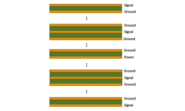
Stackup design goes beyond just layering materials; it’s about sketching a clear pathway for signal flow. A well-thought-out stackup can prevent headaches down the road. By strategically positioning ground planes and signal layers, designers can control impedance and cut down on noise. For instance, using a solid ground plane can significantly improve performance by minimizing EMI.
Here’s a quick look at how different stackup configurations can impact signal integrity:
| Stackup Configuration | Benefits | Potential Challenges |
| 4-Layer Stackup | Cost-effective, simpler design | May struggle with high-frequency signals |
| 6-Layer Stackup | Better impedance control | Increased complexity and cost |
| 8-Layer Stackup | Enhanced performance, optimized routing | Higher manufacturing costs |
By making informed choices in stackup design, designers can tackle the various challenges that high-speed PCBs present. It’s all about finding the right mix to keep your signals cruising smoothly!
Core Challenges in High-Speed PCB Stackup Design
Ensuring Signal Integrity: A Key Challenge
●Understanding Transmission Line Effects
Signal integrity often hinges on the concept of transmission lines. As signals travel along the traces, they can encounter reflections and distortions, especially at high speeds. Designers need to grasp the length and geometry of their traces to ensure that signals stay clear and accurate. For instance, using controlled impedance traces can greatly boost performance. Remember, a little knowledge goes a long way!
●Strategies for Impedance Control
Impedance control is another critical aspect of high-speed design. By maintaining consistent impedance throughout the stackup, designers can dodge reflections that lead to data loss. Utilizing differential pairs and controlled trace widths are effective strategies to keep impedance stable. In the world of PCBs, consistency is king!
| Impedance Control Strategies | Benefits | Challenges |
| Differential Pairs | Reduces crosstalk | Requires careful layout |
| Controlled Trace Widths | Enhances signal integrity | Needs precise fabrication |
Layer Stackup Considerations: Navigating Challenges
●Selecting Appropriate Dielectric Materials
Choosing the right dielectric materials is key to optimizing performance in high-speed PCB stackup design. Low-dielectric constant (Dk) materials can help reduce signal loss, but they often come with a higher price tag. Designers need to evaluate the pros and cons carefully to tailor their material selection to specific application needs. For instance, a mix of materials—like combining a low-Dk substrate with standard materials—can help strike a balance between cost and performance. It’s all about finding that sweet spot!
| Material Type | Dk Value | Cost Consideration | Application Suitability |
| Standard FR-4 | ~4.4 | Low | General Applications |
| Low-Dk Material | ~2.2 | High | High-Speed Designs |
| PTFE | ~2.1 | Very High | RF Applications |
●Mitigating Electromagnetic Interference (EMI)
EMI can be a real thorn in the side of high-speed signals. To keep those signals running smoothly, designers can implement effective strategies to reduce EMI. Techniques like proper grounding, using shielding, and maintaining a solid return path can work wonders. For example, creating a ground plane below sensitive traces can significantly reduce interference. Remember, when it comes to EMI, a stitch in time saves nine!
| EMI Mitigation Strategy | Description | Benefits |
| Ground Planes | Layer of copper beneath signal layers | Reduces EMI exposure |
| Shielding | Using conductive materials to block interference | Protects sensitive signals |
| Controlled Return Path | Ensuring return currents have a clear path | Improves signal integrity |
Advanced Routing Techniques to Address Challenges
●High-Speed Signal Routing Best Practices
Effective routing techniques are essential for maintaining signal integrity in high-speed PCB designs. Utilizing shorter trace lengths and minimizing the number of vias can significantly reduce the risk of signal degradation. For example, if a designer routes a critical high-speed signal directly from a chip to a connector without unnecessary turns or vias, it can improve performance. Moreover, placing critical signals in the inner layers can help shield them from external interference, keeping those signals running smoothly. Remember, when it comes to routing, less is often more!
| Routing Technique | Description | Benefits |
| Short Trace Lengths | Keeping traces as short as possible | Reduces signal loss |
| Minimized Vias | Using fewer vias to maintain signal quality | Improves integrity |
| Inner Layer Routing | Routing critical signals in inner layers | Shields from interference |
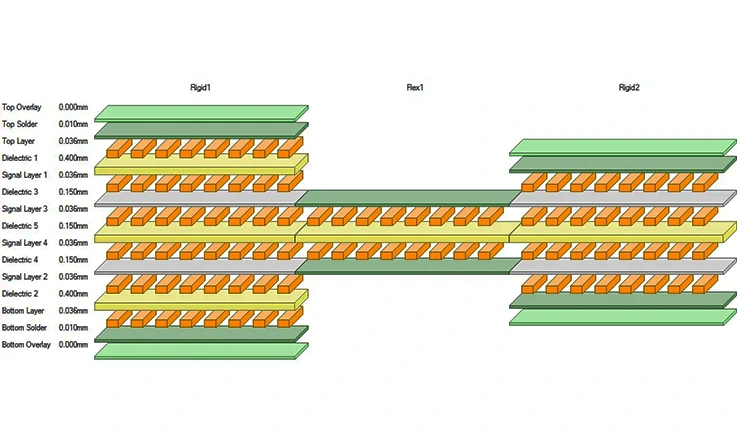
●Types of Vias in Stackup Design
Not all vias are cut from the same cloth. Different types of vias, such as blind and buried vias, come with unique advantages tailored for high-speed designs. For instance, blind vias connect outer layers to inner layers without penetrating the entire stackup, saving space and allowing for more efficient routing. Buried vias, on the other hand, are completely contained within the stackup, which can enhance performance by minimizing signal path length. Understanding the characteristics of each via type helps designers make informed choices for their specific stackup requirements. Choose wisely, and you’ll be a step ahead!
| Via Type | Description | Advantages |
| Blind Via | Connects outer layers to inner layers | Space-saving design |
| Buried Via | Located entirely within the stackup | Minimizes signal path |
| Through-Hole Via | Extends through the entire board | Easy to manufacture |
Layer Count Challenges in High-Speed PCB Stackup Design
●Low Layer Count Stackups
Using fewer layers can certainly help cut costs and simplify the design, but it often presents challenges when it comes to achieving high-speed performance. Designers need to think carefully about their stackup configuration to strike the right balance between performance and practicality. For instance, a four-layer stackup might work for basic applications, but when dealing with high-frequency signals, more layers may be necessary to really crank up performance. Finding that sweet spot is where the magic happens!
| Layer Count | Pros | Cons |
| 2-4 Layers | Cost-effective, simpler design | Limited performance for high-speed |
| 6+ Layers | Enhanced signal integrity | Higher complexity and cost |
●Moderate Layer Counts
Moderate layer counts often hit the sweet spot for high-speed applications. By placing layers strategically, designers can improve signal integrity while keeping an eye on costs. The trick is to balance performance with budgetary needs. Think of it like walking a tightrope—you want to keep everything steady without tipping the scales!
| Layer Count | Benefits | Considerations |
| 4-6 Layers | Good performance for many applications | Need to manage layer placement |
Strategy for grouping layers up to higher layer counts
●More Advanced Stackup Configurations
Advanced stackup configurations can elevate high-speed designs to new heights. Techniques such as blind and buried vias, along with impedance-controlled layers, enable designers to push the limits of performance. However, these advanced options come with their own set of challenges, and it’s essential to have the right expertise to implement them effectively. Remember, don’t bite off more than you can chew—careful planning is key!
| Configuration Type | Features | Best Used For |
| Blind Vias | Connects outer to inner layers | Space-saving design |
| Buried Vias | Located within the stackup | Enhanced signal integrity |
| Impedance-Controlled | Maintains consistent impedance | High-speed applications |
Translate Product Constraints into Stackup Needs
●Start With Board and Layer Thicknesses
The foundation of any stackup lies in the board and layer thicknesses. Designers should kick off their projects by defining these parameters based on application requirements. These thicknesses impact overall impedance and performance characteristics of the PCB. Get this right, and you’re setting yourself up for success!
| Parameter | Typical Values | Impact on Performance |
| Board Thickness | 0.8 mm to 1.6 mm | Influences impedance and thermal performance |
| Layer Thickness | 0.5 mm to 1.0 mm | Affects signal integrity and loss |
●When Should You Use PTFE or Low-Dk Materials?
PTFE and low-Dk materials can be game-changers in high-speed designs. However, they come with trade-offs. Designers need to assess when these materials are necessary and how they fit into the overall stackup strategy. It’s all about knowing when to go for it and when to play it safe!
| Material Type | Advantages | Considerations |
| PTFE | Low loss, good high-frequency performance | Higher cost |
| Low-Dk Materials | Reduced signal loss | Requires careful handling |
●Balance Loss and Dk Value
Finding the right balance between loss and Dk value is key. High-speed signals can take a hit if the Dk is too high. Designers must thoroughly analyze their stackup to identify the best trade-off for their specific application. It’s about making the right moves to keep performance in check!
| Dk Value | Signal Loss Impact | Ideal Use Case |
| High Dk (>4.0) | Increased signal loss | Low-speed applications |
| Low Dk (<3.5) | Reduced signal loss | High-speed and RF applications |
●If Low-Dk Isn’t Always Needed, Why Do RF Designers Use It?
RF designers often turn to low-Dk materials for specific applications, such as antennas and RF amplifiers. Grasping the unique needs of RF design can empower PCB designers to make smart choices about material selection. Remember, knowledge is power, and it pays to stay informed!
| Application Type | Common Uses | Reason for Low-Dk Materials |
| Antennas | Signal transmission | Reduces interference and loss |
| RF Amplifiers | Signal boosting | Enhances overall efficiency |
Procurement Considerations in High-Speed PCB Stackup Design
Evaluating PCB Suppliers to Meet High-Speed Design Challenges
●Key Criteria for Supplier Selection
Choosing the right PCB supplier is a big deal. Factors like manufacturing capabilities, quality control processes, and lead times can truly make or break a project. Designers should do their homework to find suppliers that match their high-speed design needs. Checking out recommendations and diving into case studies can provide some solid insights. When it comes to supplier selection, knowledge is your best buddy!
| Criteria | Considerations | Impact on Project |
| Manufacturing Capabilities | Ensure they can handle high-speed requirements | Avoid delays and quality issues |
| Quality Control Processes | Look for certifications and reviews | Guarantees product reliability |
| Lead Times | Understand their turnaround times | Impacts project schedule |
●Understanding Cost vs. Quality Trade-offs
In the PCB manufacturing world, cost and quality often go hand in hand. While it’s tempting to pick the lowest bid, designers should consider the long-term implications. Finding a reliable supplier that strikes a balance between cost and quality is essential for high-speed PCB projects. Remember, sometimes you have to spend a little to save a lot!
| Cost Factor | Pros | Cons |
| Low-Cost Suppliers | Budget-friendly | May compromise quality |
| Established Suppliers | Reliable quality and service | Higher costs |
Collaboration Between Design and Procurement to Navigate Challenges
●Importance of Early Involvement
Bringing procurement into the design phase can yield some serious benefits. Collaborating early ensures that the stackup meets not only performance requirements but also manufacturing feasibility. This proactive approach can prevent costly redesigns later on. After all, teamwork makes the dream work!
| Collaboration Aspect | Benefits | Potential Pitfalls |
| Early Involvement | Aligns design with supplier capabilities | May require more initial time investment |
●Effective Communication Strategies
Clear communication between design and procurement teams is vital for project success. Keeping those lines of dialogue open ensures that everyone is on the same page, minimizing misunderstandings and keeping projects on track. Remember, it’s all about keeping the buzz alive!
| Communication Strategy | Tips | Expected Outcomes |
| Regular Check-Ins | Schedule weekly updates | Ensures alignment and timely feedback |
| Shared Documentation | Use collaborative platforms | Reduces miscommunication |
Advanced Strategies to Meet High-Speed PCB Stackup Design Challenges
Leveraging HDI Techniques for Enhanced Performance
●Utilizing Microvias Effectively
Microvias can significantly boost high-speed PCB design by enabling efficient routing and improved layer interconnectivity. They reduce the PCB’s overall footprint while enhancing performance. However, to harness their full potential, designers need to grasp the nuances of microvia technology. Get savvy with microvias, and you’ll be cruising ahead!
| Feature | Standard Vias | Microvias |
| Diameter | > 0.3 mm | < 0.15 mm |
| Layer Count | 2-3 layers | 4-20 layers |
| Routing | Limited | Flexible |
| Applications | General use | High-density designs |
●Best Practices for Layer Configuration
Effective layer configuration can greatly influence performance. Strategically placing ground planes and signal layers helps optimize signal integrity and minimize crosstalk. Following established best practices in layer configuration is essential for high-speed PCB stackup success. Layer it up, and keep the signals flowing!
●Key Layer Configuration Tips:
Ground Planes: Position ground planes adjacent to signal layers to reduce EMI.
Signal Layer Arrangement: Alternate signal and ground layers to maintain a balanced stackup.
Keep Vias to a Minimum: Limit via usage to maintain signal clarity.
Selecting the Right PCB Design Tools to Address Challenges
PCB Design Software: Key Features to Consider
Choosing the right EDA PCB design software can make all the difference in high-speed stackup design. Look for features like simulation capabilities, intuitive interfaces, and comprehensive libraries. Investing in solid tools can smooth out the design process and boost overall efficiency. Remember, the right tools can be your secret weapon!
●Table: Key Features to Look for in PCB Design Software
| Feature | Description | Benefits |
| Simulation Capabilities | Allows testing designs virtually | Identifies issues early |
| User-Friendly Interface | Easy navigation and functionality | Reduces learning curve |
| Robust Libraries | Extensive component databases | Saves design time |
Importance of Simulation in High-Speed Design
Simulation is a valuable asset for high-speed PCB design. By modeling different scenarios, designers can test their stackup choices before hitting the production line. This proactive mindset can reveal potential pitfalls and save time and resources down the road. Don’t overlook simulations—they’re your safety net!
●Example of Simulation Benefits
For instance, a designer might simulate signal integrity across multiple layers to pinpoint where reflections could occur. This not only saves time in troubleshooting later but also ensures a smoother path to production.
Applications and Case Studies of High-Speed PCB Stackup Design
Learning from Successful High-Speed PCB Projects
Real-world case studies provide valuable lessons in the realm of high-speed PCB stackup design. For example, a recent project focused on a telecommunications device demonstrated the advantages of using low-Dk materials to improve signal integrity. By digging into these projects, designers can take a page from the playbook of their predecessors and apply those insights to their own designs. Learn from the best and make your mark!
●Table: Key Insights from Successful Projects
| Project Type | Key Insight | Application |
| Telecommunications | Use of low-Dk materials for signals | Enhanced signal integrity |
| Consumer Electronics | Layer stacking for EMI reduction | Improved overall performance |
Key Takeaways for Future High-Speed PCB Designs
As technology evolves, designers need to keep an eye on emerging trends and techniques. Analyzing past projects can serve as a roadmap for success in high-speed PCB stackup design. Stay ahead of the curve and adapt to changes!
●Example of Adapting to Trends
For instance, a designer might explore the incorporation of HDI techniques to meet increasing demands for miniaturization. This approach can lead to innovative designs that push the envelope in performance and efficiency.
Wrapping Up: Embracing the Future of High-Speed PCB Stackup Design
The landscape of high-speed PCB stackup design is ever-evolving, driven by technological advancements and increasing demands for performance. As we look to the future, it’s clear that the journey is filled with challenges, but with the right strategies, tools, and mindset, designers can tackle these obstacles head-on. The key lies in a collaborative approach that bridges design and procurement, ensuring that all aspects of the project align for success.
High-speed PCB stackup design is not just a technical challenge; it’s a journey that requires creativity, expertise, and collaboration. As you gear up for your next project, remember: it’s all about teamwork, staying sharp, and thinking outside the box. Don’t shy away from experimenting with new techniques and materials—after all, that’s where innovation sparks!
So, roll up your sleeves, embrace the challenges, and let’s push the boundaries of what’s possible in high-speed PCB design. Together, we can pave the way for the next generation of electronic devices that power our world. Let’s get out there and make it happen!
Frequently Asked Questions (FAQs)
What are the main challenges in high-speed PCB stackup design?
The primary challenges include ensuring signal integrity, managing impedance, and selecting appropriate materials. Designers must navigate these hurdles to achieve optimal performance.
How does the choice of materials affect stackup performance in high-speed designs?
Material selection plays a crucial role in determining signal loss, impedance, and overall performance. Choosing the right materials can significantly impact the effectiveness of the stackup.
What tools are essential for effective high-speed PCB stackup design?
Essential tools include advanced PCB design software with simulation capabilities and features for managing layer configurations. These tools can streamline the design process and enhance overall efficiency.
How can procurement professionals contribute to overcoming challenges in PCB projects?
Procurement professionals can help by ensuring that design needs align with manufacturing capabilities. By engaging early in the design process, they can provide insights into material availability, cost considerations, and lead times. This collaboration minimizes miscommunication and ensures that the final product meets both design specifications and budgetary constraints.
What role does simulation play in high-speed PCB design?
Simulation plays a vital role in high-speed PCB design by allowing engineers to test and validate their designs before physical manufacturing. It helps identify potential issues related to signal integrity, electromagnetic interference, and thermal performance, enabling designers to make informed decisions and adjustments early in the process.
Why is layer count important in high-speed PCB stackup design?
Layer count affects the overall performance and complexity of high-speed PCBs. A higher layer count can improve signal integrity by providing more routing options and dedicated ground planes, while a lower layer count may simplify design and reduce costs but could introduce performance challenges.
How can designers balance cost and performance in high-speed PCB stackup design?
Designers can balance cost and performance by strategically selecting materials, optimizing layer configurations, and leveraging advanced routing techniques. Conducting a thorough cost-benefit analysis can help identify areas where performance can be enhanced without significantly increasing costs.


