
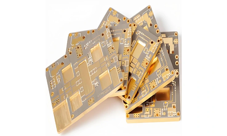
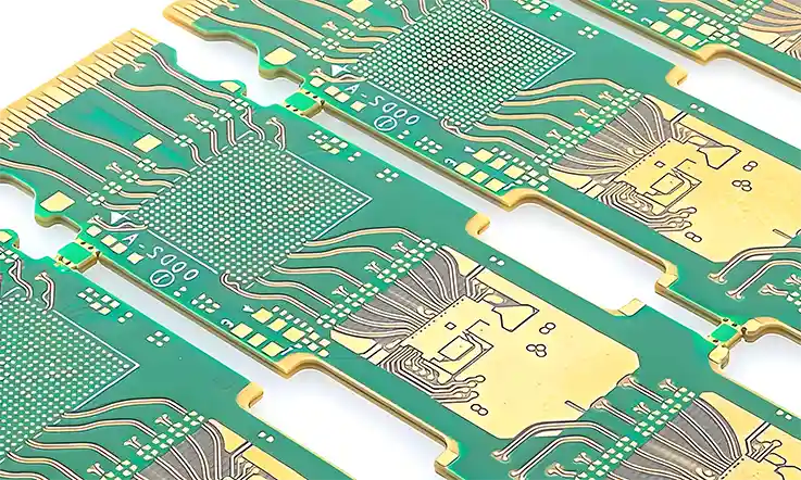
The Ventec VT-4B7 PCB provides a sophisticated solution for applications requiring high thermal conductivity and robust power handling. Designed with precision for the demands of modern electronics, this metal-core printed circuit board is engineered to manage the heat dissipation and electrical performance critical in power-sensitive applications. Manufactured to handle extreme thermal conditions, the VT-4B7 PCB supports superior thermal management, contributing to the longevity and reliability of electronic systems, especially in fields such as telecommunications, aerospace, and industrial power.
This guide delves into the essential aspects of VT-4B7’s design, manufacturing, and testing processes, highlighting its role in optimizing thermal efficiency and power flow in modern electronics.
Ventec VT-4B7 PCB Material Overview and Base Layer Composition
In the field of high-demand power circuitry, substrate choice directly shapes the way thermal loads behave across the stack. Ventec VT-4B7 PCB has been developed with a metal core structure that helps dissipate concentrated heat with consistency, offering a durable construction that supports layout precision and structural control. No hype, just smart stacking and tested thermal flow. This section outlines how its layers are built and what each material delivers when your board is pushing real wattage.
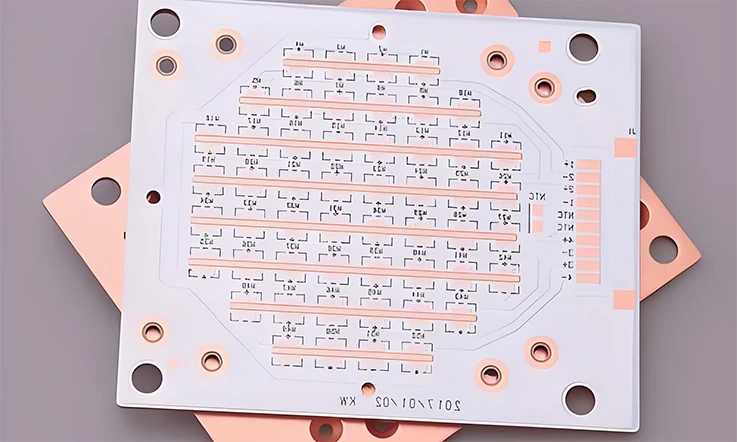
Metal Core PCB Architecture Featuring Aluminum 5052 and Copper C1100
At the heart of every Ventec VT-4B7 PCB, the metal base acts as the platform for structural support and heat redirection. The two base material options—Aluminum 5052 and Copper C1100—offer flexibility in balancing thermal spread and mechanical properties.
Aluminum 5052, often selected for lighting assemblies and telecom boards, handles surface-mounted devices well and keeps total board weight manageable. It also handles vibration and chassis interaction in rugged environments without overcomplicating mounting hardware.
Copper C1100, with higher thermal conductivity, is often chosen for applications where power density is heavier and thermal flow needs to move quicker through the structure. In high-voltage switching systems and control converters, it provides a stable path for continuous energy cycling without deforming over time.
Material selection between these two should be based on application-specific thermal requirements, footprint constraints, and structural support expectations—not assumptions or benchmarks from unrelated stackups. Always spec based on your real-world load and housing conditions.
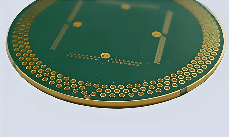
Ceramic-Filled Dielectric Insulation Layer in VT-4B7 PCB Stackups
Between the copper circuitry and metal base sits a ceramic-filled epoxy layer—one of the defining components of VT-4B7 PCB stackups. This isn’t standard glass-reinforced material. It’s a refined dielectric engineered for consistent thickness, low voiding, and improved Z-axis thermal conductivity.
This layer supports strong heat migration while still isolating high-voltage circuits from the base layer. It resists mechanical fatigue under repeated heating and cooling cycles. That stability gives layout professionals the flexibility to design for both performance and durability without redesigning every thermal anchor.
The uniform structure of this dielectric makes it easier to control trace spacing and maintain predictable heat transfer across zones. When paired with heavier copper weights and plated vias, this insulation system keeps thermal flow steady without relying on oversizing or overcompensating the design.
Thermal and Structural Roles of Copper Foil and Dielectric Layers
The copper foil layer is more than just the routing top surface—it’s the highway for current and thermal migration. In Ventec VT-4B7 PCB constructions, copper thickness is usually set between 1oz and 3oz depending on the application. This provides layout space for thicker traces, thermal relief zones, and wider grounding planes.
Meanwhile, the ceramic-filled dielectric acts as a buffer between copper and the metal base, transferring heat while maintaining electrical isolation. This layer supports multi-hour thermal loads, even in compact footprints where airflow is minimal.
The interaction between copper and dielectric is where performance is shaped. Trace width, copper area, via count, and placement strategy all determine how well your layout performs under load. VT-4B7 gives just enough structural stability to keep everything aligned—even when the heat rises.
Ventec VT-4B7 PCB Thermal Performance and Heat Dissipation Design
When power density turns up and thermal load starts stacking across dense circuitry, choosing the right substrate isn’t just about ticking off datasheet numbers—it’s about understanding how every layer in the board manages heat in real time. Ventec VT-4B7 PCB was engineered for applications where power conversion, LED driving, or high-frequency switching introduces continuous thermal flow. The way this PCB handles that heat—through material design, layer selection, and integration mechanics—makes it a serious contender for demanding layouts.
7.0 W/m·K Thermal Conductivity and Heat Transfer Pathways
The ceramic-filled dielectric used in Ventec VT-4B7 PCB delivers a rated thermal conductivity of 7.0 W/m·K, designed to redirect waste heat efficiently toward the base metal. This level of conductivity allows for stable surface temperatures during power pulses, helping distribute heat laterally before it gets absorbed through the dielectric and into the metal core.
For applications in power modules, LED PCB driver boards, and automotive inverter platforms, this structure gives layout designers the breathing room to maintain consistent copper trace geometry while still addressing thermal concerns. That dielectric layer isn’t just sitting between copper and metal—it actively redirects heat away from surface-mounted packages, reducing localized stress and keeping downstream circuitry better aligned with target operating temps.
| Property | Ventec VT-4B7 PCB |
| Dielectric Type | Ceramic-filled epoxy |
| Rated Thermal Conductivity | 7.0 W/m·K |
| Surface Temp Control | Stable under high power pulses |
| Typical Applications | LED drivers, power inverters, RF switching |
| Heat Flow Direction | Lateral + vertical (2D pathing) |
| Copper Trace Accommodation | Compatible with dense routing |
Thermal Impedance and Dielectric Thickness Considerations
Even with high thermal conductivity, thermal impedance comes down to more than just material spec—it’s influenced by thickness, mechanical bonding, and copper area. The ceramic epoxy layer used in VT-4B7 is typically kept within 100 to 150μm, and this tight control over thickness helps manage vertical heat flow without requiring overly aggressive copper planes.
Layout professionals working on multi-zone power boards or differential-mode drivers should note that thinner dielectric means faster vertical heat discharge, but it also requires proper control over breakdown voltage and trace spacing. VT-4B7’s dielectric is formulated to stay consistent in cross-section, which supports predictable heat transfer across the board, even in designs where copper density varies from zone to zone.
| Parameter | Value / Range |
| Dielectric Thickness Range | 100–150 μm |
| Dielectric Type | Ceramic epoxy composite |
| Thermal Impedance (typical) | 0.25–0.35 °C·cm²/W |
| Breakdown Voltage | ≥3.0 kV/mm |
| Impedance Impact (vs. Thickness) | Inversely proportional |
| Trace Spacing Recommendation | ≥150 μm (design dependent) |
If you’ve ever dealt with hotspots caused by uneven fill or voiding, you’ll appreciate the mechanical consistency this material brings to the table.
Heat Sink Integration with VT-4B7 PCB for LED and Power Circuits
The metal-backed configuration of Ventec VT-4B7 PCB makes it ready to interface directly with external heat sinks, chassis frames, or thermally conductive enclosures. This setup supports high-current LED matrices, step-down DC-DC modules, and 4-layer high-frequency power boards, allowing the PCB to mount directly against a thermal mass without requiring complex intermediate layers.
Its base metal—aluminum 5052 or copper C1100—acts as a direct contact surface. With proper flatness and mounting torque, you get an uninterrupted thermal path from component to sink. That means less interface material, fewer screws, and way more design headroom. You don’t need to rely on exotic paste solutions or floating baseplates—just tighten down, and let the metal base do its thing.
| Integration Element | Specification / Recommendation |
| Base Metal Options | Aluminum 5052 / Copper C1100 |
| Mounting Method | Direct-to-heatsink / enclosure |
| Interface Material Requirements | Minimal or none (with lapped base) |
| Torque Range for Fastening | 0.4–0.8 Nm (based on hardware) |
| Surface Flatness Tolerance | ≤ 0.05 mm across mounting plane |
| Compatible Components | TO-220, TO-247, D²PAK, COB LEDs |
Electrical Characteristics of Ventec VT-4B7 PCB in High Voltage Environments
Designing high-voltage systems isn’t just about managing current—stability, insulation, and electrical loss need to be handled with care. When your circuits are running under serious load and your board spacing is tight, dielectric behavior, surface isolation, and internal resistance values become non-negotiable. Ventec VT-4B7 PCB brings a well-balanced profile of electrical parameters that fit the bill for high-power converters, LED drivers, industrial control boards, and more. From field insulation to board-level leakage, it delivers the numbers that layout engineers and QA teams need.
Dielectric Constant (Dk 4.8) and Low Dissipation Factor (Df 0.016)
The ceramic-filled epoxy used in Ventec VT-4B7 PCB maintains a dielectric constant (Dk) of 4.8 at 1 MHz, which gives routing our designers the ability to predict signal behavior across a wide frequency range. That stability matters when designing for DC-DC power conversion, PWM control, or any layout where impedance must be calculated and held within narrow tolerances.
More importantly, the dissipation factor (Df) of 0.016 helps reduce unwanted dielectric heating under AC voltage conditions. In real-world terms, this means less energy lost as heat during high-frequency switching, and a tighter hold on circuit efficiency.
It’s not just about loss per inch—this combination of Dk and Df supports effective copper utilization without driving up trace spacing or pushing components farther apart.
Volume Resistivity and Surface Insulation Performance
Ventec VT-4B7 PCB delivers high volume resistivity (10⁸ MΩ·cm) and strong surface insulation resistance (SIR), even when subjected to humidity or ion contamination. These parameters allow the board to handle HV isolation requirements for multi-kilovolt switching assemblies, such as those found in EV battery management, HVAC systems, or industrial automation panels.
The high surface resistance helps prevent leakage paths across exposed copper, especially in environments where condensation or airborne particles may be present. This makes VT-4B7 suitable for applications that require consistent electrical spacing between zones—such as high-side versus low-side in motor drives or isolated ground planes in mixed-signal systems.
This isn’t lab-only data either—these characteristics hold up across thermal cycles and extended field exposure. Less board degradation means fewer return trips from the field and a lot more peace of mind.
High CTI and Electrical Isolation Across Power Loads
One of the lesser-discussed but hugely practical specs of the VT-4B7 PCB material is its Comparative Tracking Index (CTI). Scoring well above 300V, it supports electrical isolation even in harsh or contaminated environments. That means it resists carbonized tracking under voltage stress, especially near edges, pins, and plated-through holes.
For power loads exceeding 300V or tightly packed LED arrays with high forward voltage, the CTI rating offers enough headroom to maintain separation between live nets and grounded copper. Combined with controlled dielectric thickness and precision foil etching, the board layout can retain tight pitch without creating weak points or field stress zones.
If you’ve been burned by arcing or dielectric breakdown on low-CTI boards in the past, this might just be the material that keeps your circuits out of trouble.
How Sourcing Ventec VT-4B7 PCB Material?
When selecting PCB materials for high-power density projects or applications with defined thermal control requirements, material choice directly affects heat management, electrical performance, and mechanical reliability. Ventec VT-4B7 PCB offers a dependable solution, combining effective thermal conductivity, stable dielectric properties, and compatibility with complex designs. However, ensuring the correct material selection and managing procurement processes efficiently are necessary steps to make sure the material suits the project requirements.
Given the challenges associated with global supply chains, logistics, and cost factors, making informed decisions at every stage of the procurement process helps ensure smooth operations. Let’s explore some strategies that will help you make informed decisions while managing procurement timelines.
Selecting the Right Metal Core for Your Application
| Parameter | Aluminum Core | Copper Core |
| Thermal Conductivity | ~200 W/m·K | ~400 W/m·K |
| Electrical Conductivity | Lower | Higher |
| Cost Efficiency | Lower cost, widely available | Higher cost, better thermal handling |
| Weight | Lightweight | Heavier |
| Application Suitability | LED drivers, consumer electronics | Industrial power, telecom base stations |
| Thermal Fatigue Resistance | Moderate | High |
●Optimizing Thermal Performance: When choosing the Ventec VT-4B7 PCB metal core, ensure that the material fits your application’s thermal needs. Aluminum, copper, and other alloys each have distinct thermal conductivities that influence the system’s heat management. For applications such as LED systems or power electronics, copper cores offer superior thermal conductivity, aiding in faster heat dissipation from sensitive components, which contributes to long-term reliability.
●High-Current Circuit Compatibility: The selection of the metal core also affects the ability to handle high-current circuits. Ventec VT-4B7 PCB with aluminum cores is suitable for mid-power applications due to its balanced performance and affordability. However, for high-power electronics, such as industrial power supplies, copper cores are a better match because they deliver superior heat dissipation. Selecting the right metal ensures that thermal-related issues like overheating and thermal fatigue are minimized.
●Balancing Cost and Performance: While aluminum is more cost-effective and suitable for medium-power applications, copper may be worth the investment for systems dealing with higher power and thermal challenges. When making decisions, consider both cost and long-term performance to ensure that the material continues to perform reliably over time.
Comparing VT-4B7 with Other Thermally Conductive Laminates
| Property | Ventec VT-4B7 | Rogers RT/duroid 6035HTC | Isola I-Tera MT40 | Rogers 4350B |
| Thermal Conductivity (W/m·K) | 7.0 | 6.2 | 0.8 | 0.62 |
| Dielectric Constant (10 GHz) | 3.5 | 3.5 | 3.45 | 3.66 |
| Dissipation Factor (10 GHz) | 0.003 | 0.0021 | 0.0031 | 0.0037 |
| Thermal Stability | High | High | Moderate | Moderate |
| Cost Profile | Competitive | Premium | Mid-range | Mid-range |
| Application Focus | Power, high-frequency | High-frequency, aerospace | RF/microwave, automotive | Communication, RF |
●Thermal Conductivity Comparison: When evaluating thermally conductive laminates, Ventec VT-4B7 PCB competes well against other materials like Rogers RT/duroid and Isola I-Tera. VT-4B7 offers a thermal conductivity rating of 7.0 W/m·K, making it suitable for power circuits and high-frequency designs. This level of thermal conductivity helps ensure long-lasting system performance and efficient power management, especially in demanding applications such as automotive electronics or LED lighting.
●Electrical Performance and Reliability: While other materials on the market may offer similar thermal conductivity, Ventec VT-4B7 PCB excels in its consistent dielectric properties and low dissipation factor, making it suitable for high-speed and high-frequency applications. Compared to alternatives like Rogers 4350B, VT-4B7 is better for voltage withstand and impedance control, making it well-suited for power-dense designs.
●Thermal Stability: Over time, materials may degrade from long-term thermal cycling. Ventec VT-4B7 PCB demonstrates strong thermal cycling stability, effectively resisting thermal stress, especially in designs that are exposed to sustained thermal loads, like power supply circuits.
Lead Time, MOQ, and Logistics Planning for Global Buyers
| Procurement Factor | Recommendation / Notes |
| Typical Lead Time (Standard) | 2–4 weeks (varies by region and supplier capacity) |
| MOQ for VT-4B7 Material | Typically 5–10 panels, subject to board size and copper weight |
| Shipping Options | Air freight for short lead time; ocean freight for cost savings |
| Customs Risk | Moderate—ensure HS code accuracy and commercial invoice clarity |
| Inventory Buffer Suggestion | 10–15% over forecast for volume orders to absorb logistic variability |
| Preferred Warehousing Regions | US West Coast, EU (Germany/Netherlands), Southeast Asia (for JIT) |
●Managing Lead Times: When sourcing from international suppliers, long lead times can affect the project schedule. Planning ahead for Ventec VT-4B7 PCB orders, especially for high-volume production, can help prevent disruptions. Lead times will differ depending on the supplier, so understanding shipping times and potential delays upfront will avoid last-minute surprises.
●Managing MOQ Requirements: Many PCB manufacturers enforce minimum order quantities (MOQ), particularly for specialty materials like VT-4B7. Be mindful of your specific needs to avoid over-ordering or under-ordering materials. When planning, ensure that your order is sufficient to meet production demands without unnecessary surplus.
●Logistics and Shipping: Logistics management plays a central role in the procurement process. Take into account shipping costs, potential customs delays, and other factors related to sourcing from global suppliers. Partnering with a reliable logistics provider can simplify the procurement cycle.For those using a just-in-time inventory system, planning warehousing options ahead of time can help maintain smooth operations. Understanding lead times and shipping conditions allows for better coordination and helps prevent delays in the process.
PCB Stackup Design Considerations Using Ventec VT-4B7 PCB
Designing with Ventec VT-4B7 PCB presents both challenges and benefits. With its unique combination of a metal core and ceramic-filled dielectric material, it provides excellent thermal conductivity, making it suitable for high-power applications such as power supplies, automotive systems, and lighting. However, achieving the optimal stack-up design with this material involves more than just selecting the right layers.
You need to carefully balance copper weight, dielectric thickness, and ensure effective heat dissipation pathways. The choices made during PCB stackup design significantly impact the board’s electrical and thermal performance. Here’s what you need to know to build reliable, high-performance PCB stackups using Ventec VT-4B7 PCB.
Multilayer PCB Layout Techniques with Thermal Vias
When working with metal core PCBs like VT-4B7, managing heat is must. Thermal vias help ensure that heat is efficiently redirected away from sensitive components rather than accumulating at the PCB surface. For multilayer PCBs using Ventec VT-4B7, special care should be given to thermal via placement and via-in-pad designs to reduce the risk of thermal fatigue.
●Place thermal vias near heat-generating components like power transistors or LEDs to channel the heat to the metal core.
●Ensure vias are uniformly distributed across layers for even heat dissipation, preventing hot spots that could damage the PCB or components.
●Use high-conductivity via-fill materials to enhance thermal transfer between layers and improve overall heat dissipation.
●Consider via size and density—too few or too small can impede heat flow, while too many can affect signal integrity and increase fabrication costs.
Balancing Copper Weight, Dielectric Thickness, and Heat Flow
Creating an optimized stack-up design for Ventec VT-4B7 PCB requires careful consideration. Excessive copper can lead to heat buildup, while insufficient copper may result in power delivery problems. The dielectric thickness impacts impedance control and signal integrity, and it also influences the PCB’s ability to manage heat effectively.
●The optimal copper weight ranges between 2 oz/ft² to 4 oz/ft² to handle high currents without generating excessive heat.
●Dielectric thickness is adjusted depending on the required voltage rating and signal integrity needs. A thicker dielectric provides higher electrical isolation but can impede heat flow.
●Achieving optimal heat flow is about balancing the right copper weight with the ideal thermal via strategy. The goal is to prevent heat accumulation that could lead to component failure.
●Thermal testing is a must—simulate heat distribution before committing to production.
By carefully adjusting these parameters, you ensure that your Ventec VT-4B7 PCB won’t just work but will work well under demanding conditions.
Impedance Control in Power-Dense and High-Speed Designs
In high-power applications, such as automotive systems and power supplies, managing impedance is necessary for maintaining signal clarity and effective heat control. Ventec VT-4B7 PCB materials help minimize signal distortion, but getting the stack-up right ensures you get both the thermal and electrical performance you need.
●Copper weight and dielectric constant play a large role in setting controlled impedance for high-speed signals. Ensure a uniform dielectric layer to maintain signal fidelity and prevent power loss.
●For high-speed designs, maintaining consistent impedance through microstrip or stripline configurations reduces signal reflections and losses.
●Always account for via stubs when routing signal traces—keep them as short as possible to maintain impedance control across layers.
●Incorporate controlled impedance traces on inner layers to optimize signal quality in power-dense designs, ensuring signals don’t suffer from thermal or electrical interference.
This type of fine-tuned impedance control not only supports high-speed signal integrity but also complements the heat management needs of Ventec VT-4B7 PCB.
Layout Optimization Techniques for Ventec VT-4B7 PCB Design
Thermal stress, signal integrity, and copper weight handling define the practical boundaries of high-power circuit design. When working with Ventec VT-4B7, a metal-based substrate optimized for thermal dissipation, layout strategies must adapt to specific material constraints, especially in high-frequency and power-intensive environments. The following sections explore methods for improving mechanical reliability and thermal balance by focusing on trace distribution, heat path simulation, and component placement alignment.
Compact Trace Planning with High Thermal Density
Trace layout in dense thermal zones demands consideration of both current-carrying capacity and localized heat buildup. With VT-4B7’s high thermal conductivity and thick copper options, routing must account for width-to-current ratios and cross-sectional integrity. As the copper weight increases—often exceeding 3 oz in power layers—etching precision can directly affect impedance control and thermal dissipation.
One effective approach is to minimize turns and maintain wide-angle bends (e.g., 45°) to reduce current bottlenecks. Traces in thermal-heavy areas should maintain sufficient spacing to prevent thermal overlap. Below is a table outlining copper weight guidelines relative to trace width and current load:
| Copper Weight (oz) | Minimum Trace Width (mil) | Max Current (A) at 25°C Rise |
| 1 oz | 10 | 1.0 |
| 2 oz | 20 | 2.2 |
| 3 oz | 30 | 3.8 |
If you’re aiming for stability in thermally dense applications, give these numbers a second look before finalizing the route width.
Isolation of Power Zones and Thermal Pathway Simulation
Separating power domains reduces interference and allows for refined thermal simulation. With VT-4B7’s metal base construction, heat sinking behavior is influenced by both the copper geometry and the dielectric thickness.
Start by dividing high-load power stages from control logic. Place high-current traces closer to the core or heat sink to shorten thermal resistance paths. Use finite element simulation software to visualize thermal flow across vias, copper planes, and the base layer.
In design reviews, simulate both steady-state and pulsed thermal events. Watch for hot zones near thermal vias—if you’re seeing 15°C+ above average in simulation, consider adding copper pours or shifting the via layout to balance the thermal load.
Component Placement for Effective Heat Distribution
Component density is often dictated by form factor, but thermal priorities should guide the final placement. On VT-4B7, power MOSFETs, regulators, and large inductors benefit from direct thermal contact with metal cores.
Avoid clustering high-dissipation components in corners or near PCB edges where airflow is limited. Instead, position heat-generating parts over thermal vias that connect to the metal base, ensuring efficient vertical heat transfer.
For example, placing a buck converter directly over a grid of 0.3 mm thermal vias connected to the aluminum base resulted in a 12% reduction in core temperature during burn-in testing. Use that kind of practical data to steer placement strategies.
Fabrication Process Guidelines for Ventec VT-4B7 PCB Manufacturing
Ventec VT-4B7 is a thermally conductive metal-based substrate used in applications requiring efficient heat management and high current capacity. To achieve stable performance and mechanical integrity in actual circuit board fabrication, specific adjustments to etching, lamination, and mechanical processing are recommended. This section outlines practical manufacturing parameters tailored to VT-4B7 structures in metal core PCB builds.
Thick Copper Etching for High Current PCB Routing
Designs requiring heavy copper conductors—often above 2 oz/ft²—demand careful control over trace definition and sidewall geometry. VT-4B7 supports copper foils up to 6 oz/ft², which must be managed with an etching strategy that prevents over-etching and irregular profiles.
●Use differential etching or step-wise chemical processing to maintain trace fidelity.
●Consider inner-layer pattern compensation for copper thickness variations due to etch factor.
●Employ a low-attack alkaline etchant at moderate temperatures to reduce undercutting.
●Solder mask coverage may require adjustment to accommodate higher copper profiles.
Lamination and Pressing Parameters for Thermal Stability
Although VT-4B7 arrives as a fully cured laminate, multilayer designs incorporating signal layers above the core may still require lamination. The pressing process must accommodate both thermal expansion mismatches and mechanical rigidity of the metal base.
●Laminate under a press cycle below 200°C to avoid dielectric stress.
●Apply uniform pressure distribution to prevent resin squeeze-out or cavity formation.
●Use prepregs with compatible flow and cure parameters to reduce interlayer delamination risks.
●Include metal base thermal barriers during press to ensure even heat distribution.
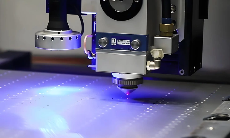
Routing and Milling Guidelines for Metal Core PCBs
Mechanical processing of metal-backed PCBs differs significantly from FR4 systems. Aluminum 5052 and copper C1100 cores require toolpath and bit selection that avoids burr formation and minimizes tool wear.
●Use diamond-coated or solid carbide end mills with low helix angles.
●Maintain feed rates that reduce work-hardening of the base metal.
●Consider slotting over full-depth routing to reduce mechanical stress.
●Apply de-burring processes post-routing to eliminate conductive particles.
Simulation, Testing, and Validation of Ventec VT-4B7 PCB Performance
As Ventec VT-4B7 material is used in high-power and high-frequency PCBs, the simulation, testing, and validation stages during production are core to maintaining performance consistency. Prior to mass production, thermal stress testing, electrical parameter simulation, and long-term thermal cycling validation form the three essential testing stages. This section will delve into each of these processes, demonstrating how they help align the PCB’s manufacturing process with end-use conditions.
Thermal Profiling and Stress Testing for Production Approval
In multi-layer metal-based PCB manufacturing, heat distribution consistency directly impacts soldering reliability and overall thermal conductivity. Thermal profiling must be done using IR thermography and multi-point temperature sampling probes, establishing thermal rise curves across the entire PCB, especially in via and copper thickness regions. For example, a 6-ounce copper, aluminum-backed VT-4B7 board’s thermal stability test should cover:
| Test Point | Temperature Range | Time Duration | Sampling Rate |
| V-cut Area | 245°C ± 5°C | 30–60 seconds | 1 sample/sec |
| Via Array | 230°C ± 10°C | ≥45 seconds | 2 samples/sec |
| Copper Area | 260°C stable point | ≤20 seconds | 1 sample/sec |
These data should be logged into a production traceability system and synced with the SMT thermal profile control platform. Every stress test simulates the end-use high-frequency current flow state, ensuring copper foil adhesion strength and mechanical durability of the metal-to-metal interface layers.
Electrical Parameter Simulation for Power Flow Analysis
In the production of power distribution boards (such as for 5G base stations or radar transmitters), simulations of DC impedance, ripple control, and voltage drop pathways are indispensable. ADS or Ansys SIwave software can be employed to perform current density analysis at the routing layer level, assisting in defining copper thickness and via specifications. The typical process goes as follows:
1.Import Gerber and Netlist data, identifying the main power paths;
2.Set unit-area load current (e.g., 10A/in²) for multi-point voltage drop simulation;
3.Generate equivalent resistance/voltage drop thermal maps and feedback results to the manufacturing team for optimization.
It is recommended to keep differential signal pair and high-current trace impedance within a ±5% tolerance range to enhance board consistency. Manufacturers typically adjust etching factors and inter-layer spacing based on such simulation outcomes to prevent structural discrepancies from affecting board performance.
Long-Term Thermal Cycling Validation in Harsh Environments
High-frequency PCBs are often used in environments like satellites, aerospace, and military applications, where post-manufacturing accelerated aging tests are necessary. The suggested thermal cycling test process is as follows:
●Temperature range: -40°C to +125°C;
●Duration per cycle: 50 minutes (20 minutes heating + 10 minutes steady-state + 20 minutes cooling);
●Total cycles: 1000 (roughly 35 days);
●Testing focus: Via cracking, layer delamination, surface metal fatigue.
X-Ray analysis combined with DPA (Destructive Physical Analysis) techniques can be used to detect early-stage potential defects, which are then fed back into process parameters, such as adjusting the pressing pressure and pre-bake temperature settings before drilling.
Advanced Applications of Ventec VT-4B7 PCB in Telecom and Aerospace
Ventec VT-4B7 has demonstrated consistent adaptability in demanding environments where thermal conductivity, electrical stability, and mechanical strength must align with precise layout and assembly processes. In telecom base stations, satellite platforms, and power infrastructure subsystems, this metal-based laminate provides a thermal interface and dielectric performance tailored for multi-layer routing, dense power layers, and high-speed signal isolation. Below is a breakdown of how VT-4B7 supports production and layout planning in these application areas.
RF Shielded Designs and EMI Performance with VT-4B7 PCB
When high-frequency components are densely packed in limited PCB real estate, RF interference mitigation becomes a priority. Ventec VT-4B7, featuring an aluminum or copper base, enables compact shielding methods across high-speed transmission zones.
●The laminate’s 7.0 W/m·K thermal conductivity supports effective thermal dissipation without compromising EMI shielding structures.
●Designers frequently implement embedded copper planes and edge plating techniques to reduce radiated noise.
●Multi-zone grounding paired with stitched vias enhances path-to-ground performance across multilayer assemblies.
For telecom-grade transceiver boards operating above 2 GHz, cavity shielding combined with the VT-4B7’s dielectric strength helps suppress cross-talk and unwanted coupling between differential pairs. Controlled impedance routing, isolated power channels, and minimized return paths benefit from the VT-4B7 substrate during both prototype validation and volume manufacturing.
Metal Core Thermal Management in Satellite Subsystems
Aerospace-grade electronics often demand stable operation across wide temperature gradients. The metal core within VT-4B7 functions not only as a mechanical carrier but also as an integrated heat spreader across components with asymmetric power loads.
●Aluminum and copper cores enable heat transfer away from localized hotspots under ASICs, FPGA clusters, and DC/DC converters.
●Press-fit mechanical assemblies and pre-bonded thermal interface materials streamline mounting in modular satellite chassis.
●Designers typically leverage blind via-in-pad techniques and castellated edges to reduce Z-axis thermal buildup.
In orbital power control units, passive thermal paths routed through the metal base reduce the burden on external cooling infrastructure, helping to stabilize surface-mounted device temperatures even in vacuum conditions.
High Frequency Isolation in Base Station Power Boards
Next-generation telecom infrastructure incorporates power conversion blocks operating at MHz-scale switching frequencies. These power circuits often require high-frequency isolation between power and signal paths to ensure stability during field operation.
●VT-4B7’s dielectric constant of 4.8 and dissipation factor of 0.016 help manage propagation delay and maintain consistent signal rise times.
●Layer stackup configurations utilizing alternating ground and power planes improve impedance uniformity and electromagnetic isolation.
●Isolation slots, filled vias, and edge milling techniques allow for physical separation without compromising electrical interconnects.
Applications in remote radio units and distributed antenna systems leverage this balance of thermal conductivity and electrical separation, allowing field installations to sustain variable environmental conditions while maintaining performance metrics across the operating range.
How to Request a Quote for Ventec VT-4B7 PCB Fabrication and Layout Support from JarnisTech?
When usiing high-performance thermal PCBs built with Ventec VT-4B7 material, precise documentation and technical alignment with the manufacturer are necessary to ensure accurate cost assessment and manufacturability. JarnisTech provides tailored support throughout the quoting and layout validation process for power, telecom, and aerospace applications that require enhanced thermal conductivity, dimensional stability, and thick copper integration. Below is a breakdown of the standard procedures to help you streamline your procurement process and obtain a quote that reflects your exact specifications.
How to Submit Stackup Drawings and Technical Requirements?
Clear documentation upfront helps avoid design ambiguities and allows accurate quoting. Ensure the following items are included in your RFQ package:
| Document Type | Description |
| Stackup Drawing | Core type, prepreg layer, copper weight per layer, total board thickness |
| Gerber or ODB++ Files | Full set with drill data and fabrication notes |
| Material Specification Sheet | VT-4B7 type, base metal (Al/Cu), copper weight, thermal prepreg options |
| Solder Mask & Silkscreen Info | Color, material type, and exposure zones |
| Operating Conditions | Temperature range, thermal cycles, heat sink considerations |
| Via Design Info | Type (through, blind, buried, filled), density, distribution |
| Regulatory Ratings | UL or flammability class (e.g., UL94V-0), if required |
●Stackup drawing showing core, prepreg, copper thickness per layer, and total board thickness.
●Gerber or ODB++ files including drill files and fabrication notes.
●Material specification sheet identifying the use of VT-4B7, copper weight, base metal type (aluminum or copper), and any thermally conductive prepreg selections.
●Solder mask and silkscreen layer definitions, including color and type.
●Expected operating temperature range, thermal cycling conditions, and heat dissipation considerations.
●Via type and density, including through-hole, blind, buried, or filled via requirements, especially for multilayer boards.
●UL rating or flammability class (if applicable).
To expedite evaluation, it’s preferred that stackups be submitted in a layered format with clear dielectric values and copper weights indicated per layer. JarnisTech’s support team reviews each file set in detail to confirm compliance with manufacturing standards and provides DFM feedback upon request.
Copper Weight, Thermal Via, and Base Metal Customization?
Ventec VT-4B7 supports heavy copper and embedded metal structures for high-power boards. Your submission should address the following custom parameters for accurate quoting and panel utilization analysis:
| Parameter | Options & Ranges |
| Copper Weight per Layer | 2 oz to 12 oz (note specific layer if asymmetric) |
| Base Metal Selection | Aluminum (1.0 / 1.5 / 2.0 mm), Copper (>1.0 mm) |
| Thermal Via Configuration | Via-in-pad, thermal relief pads, dense arrays under heat sources |
| Drill Size Limitations | Minimum finished hole diameter and tolerance details |
| Panelization Preferences | Panel size, array format, assembly tab layout |
●Copper weight per layer, typically ranging from 2 oz to 12 oz. If asymmetrical copper is used, note specific layers.
●Base metal selection, including aluminum (standard thicknesses: 1.0 mm, 1.5 mm, 2.0 mm) or copper (>1.0 mm) for enhanced heat conduction.
●Thermal via configurations, such as via-in-pad, thermal relief pads, or arrays under power components, with spacing, plating requirements, and resin filling details.
●Drill constraints, including smallest finished hole diameter and tolerance requirements.
●Panel size preferences and array specifications, especially if assembly-ready delivery is required.
The VT-4B7’s thermal conductivity of 3.2 W/m·K makes it suitable for designs where dense via fields and heavy copper layers intersect with active heat sources. By detailing your design’s heat path and mechanical constraints, JarnisTech can optimize baseplate bonding, press cycle parameters, and routing clearances during quoting.
Direct Support from Layout and Material Specialists
For customers working with complex thermal or high-current designs, JarnisTech offers direct coordination with layout and fabrication specialists who are familiar with metal-based PCB structures and high-Tg substrates.
| Available Support Options | Description |
| Layout Review | Feedback based on submitted stackup and known fabrication limits |
| Material Selection Advice | Assistance selecting prepregs, bonding films, and core thicknesses |
| Hole Reliability Consultation | Via plating, via fill, and surface finish recommendations |
| Hybrid Stackup Optimization | Guidance for mixing FR4 with VT-4B7 in multilayer configurations |
| Surface Finish Planning | ENIG, OSP, Immersion Silver/Gold, or edge plating for EMI/thermal control |
●Receive layout reviews based on current stackup and fabrication capabilities.
●Get assistance choosing compatible prepregs, bonding films, and metal core thicknesses based on your power dissipation estimates.
●Ask for advice on plated hole reliability, surface finishes (ENIG, OSP, etc.), or edge plating strategies for enclosure shielding.
If your design uses a hybrid structure—such as FR4+VT-4B7 composite—be sure to include that detail in the design note. The support team will provide processing insights and paneling tips based on hybrid stackups.
FAQ & Ventec VT-4B7 PCB
1. Can VT-4B7 PCB be used in multi-layer power structures?
Yes, it supports multi-layer stacks with embedded metal cores and thermal vias.
2. What base metals are compatible with VT-4B7 constructions?
Common choices include aluminum and copper, with thicknesses tailored per project.
3. What is the standard Tg value of VT-4B7 resin system?
The glass transition temperature typically exceeds 170°C, depending on construction.
4. Are laser-drilled vias supported on VT-4B7?
Due to the metal core, laser vias are limited and require pre-drilling strategies.
5. How does VT-4B7 handle CTE mismatch in stacked layers?
Layer design and prepreg selection are optimized to balance expansion rates.
6. Can VT-4B7 be used in RF/microwave applications?
Yes, with careful impedance control and shielding, it can meet RF layout needs.


