
High-power electronics in automotive and industrial sectors require more than thermally conductive materials; they demand a fully realized thermal and electrical system. The performance of an advanced insulated metal substrate (IMS) like the Ventec VT-4B7SP is defined not by its material properties alone, but by the precision of its design, fabrication, and final assembly.
This guide provides a technical framework covering every stage of implementation. It analyzes material characteristics, explores design strategies for high-voltage and thermal management, and details the validation processes for demanding applications. The focus extends beyond the bare board to the interplay between the substrate, thermal interface materials, and the complete assembled system.
Ventec VT-4B7SP Substrate: Technical Specifications and Core Attributes
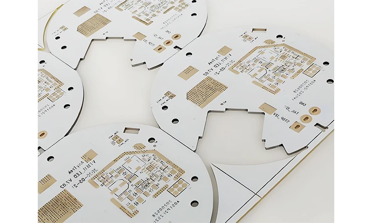
The Ventec VT-4B7SP is an insulated metal substrate (IMS) printed circuit board (PCB) that integrates an aluminum base with a ceramic-filled dielectric layer. This structure is engineered for advanced thermal management within electronic assemblies. Its material composition promotes enduring performance under rigorous operational conditions, providing a robust platform for high-power automotive, industrial, and LED lighting applications.
Core Material Features
The material and structure of the Ventec VT-4B7SP provide the following advantages for demanding applications:
●High Thermal Conductivity (7.0 W/m·K): The ceramic-filled dielectric layer efficiently dissipates heat from high-density components, which helps to extend component operating life.
●Integrated Aluminum Core: Provides robust mechanical support for the board and acts as an effective heat spreader, enhancing base-layer thermal management.
●High-Integrity Dielectric Layer: Offers sound electrical insulation while balancing the dielectric constant and dissipation factor to preserve signal clarity and prevent current leakage.
●Superior Form Factor Retention: Resists warping and distortion, preserving the flatness required during precision component mounting and soldering, thereby streamlining the assembly process.
●Adherence to Global Standards: Meets UL94 V-0 flame retardance ratings and RoHS directives, making it suitable for applications with stringent regulatory requirements.
Core Material Properties Table:
| Attribute | Specification |
| Thermal Conductivity | 7.0 W/m·K |
| Base Metal | Aluminum |
| Dielectric Layer Composition | Ceramic-filled epoxy resin |
| UL Flammability Rating | UL94 V-0 |
| RoHS Compliance | Yes |
| Surface Flatness Retention | High |
| Typical Dielectric Constant (Dk) | 6.5 @ 1 MHz |
| Dissipation Factor (Df) | ≤ 0.025 |
Thermal and Mechanical Characteristics
The VT-4B7SP substrate is engineered for exceptional heat dissipation, a fundamental trait for applications where temperature management directly impacts function and lifespan.
●Rapid Heat Transfer: The specified thermal conductivity of 7.0 W/m·K facilitates swift heat transfer from active components to the aluminum base, helping to lower operating temperatures and improve the endurance of the final assembly.
●Dielectric Thickness Options: Choices such as 0.045 mm and 0.020 mm allow for tailored thermal impedance, enabling designs to be optimized for performance under sustained current loads.
●Mechanical Fortitude: With a tensile strength exceeding 150 MPa, the material resists distortion. This results in a flat and true substrate, advantageous for automated component placement and soldering processes.
Thermal & Mechanical Data Table:
| Property | Specification |
| Thermal Conductivity | 7.0 W/m·K |
| Dielectric Thickness Options | 0.045 mm / 0.020 mm |
| Thermal Impedance | ≤ 0.3°C·in²/W |
| Tensile Strength | >150 MPa |
| Thermal Expansion Coefficient | ≤ 20 ppm/°C (z-axis) |
| Peel Strength (copper layer) | ≥ 1.8 N/mm |
| Operating Temperature Range | -40°C to +130°C |
Electrical Performance and Safety Ratings
Beyond its thermal capabilities, the VT-4B7SP provides the electrical robustness required for high-power applications. It maintains high insulation resistance and dielectric strength across wide operating temperatures.
●Breakdown Voltage Exceeding 6 kV: A high breakdown voltage offers substantial insulation between the copper circuitry and the aluminum base, a necessary feature for AC/DC drivers, inverters, and PFC boards operating under peak loads.
●Comparative Tracking Index (CTI) > 600V: The high CTI value guards against surface arcing in humid or dust-prone industrial settings, especially beneficial for designs utilizing double-sided SMT.
●UL Thermal Class Rating (130°C): This UL rating provides a verified safety margin for thermal excursions that occur during board baking, component soldering, and post-assembly testing.
Electrical Properties Table:
| Attribute | Specification |
| Breakdown Voltage | >6,000 V |
| Insulation Resistance | >10⁸ MΩ |
| Dielectric Strength | >20 kV/mm |
| Comparative Tracking Index (CTI) | >600 V |
| Surface Resistivity | ≥ 10¹³ Ω |
| Volume Resistivity | ≥ 10¹⁴ Ω·cm |
| UL Thermal Class | 130°C |
Section Highlights:
1.Core Strengths: VT-4B7SP combines high thermal conductivity (7.0 W/m·K), a robust aluminum base structure, and high-voltage insulation exceeding 6 kV.
2.Performance Assurance: Its material properties ensure superior thermal management, mechanical stability, and electrical safety, meeting stringent industrial and automotive standards.
Design and Layout Strategies for VT-4B7SP Substrates
As demands for thermal fortitude in automotive and industrial electronics increase, the structural planning of IMS boards requires more than a basic layout exercise. Strategic layer construction, material choices, and interconnection tactics help achieve performance benchmarks under heat-intensive and high-current conditions. The following topics detail practical approaches for optimizing a design for both performance and successful assembly.
Layer Configuration and Copper Weight
The architecture of a high-performance IMS board begins with a well-defined stack-up. Decisions made here directly affect current-carrying capacity, impedance characteristics, and the mechanical character of the final board.
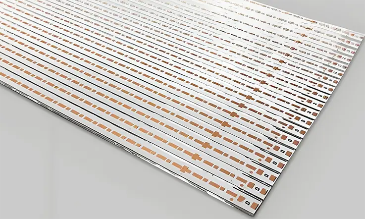
●Copper Foil Thickness: Options, typically from 1oz to 3oz, should be selected to align with the application’s expected current load and heat distribution requirements.
●Dielectric Layer Thickness: The thickness of the ceramic-filled insulating layer influences both thermal impedance and the board’s overall deflection tolerance under mechanical stress.
●Inter-layer Adhesion: Strong adhesion between the copper, dielectric, and aluminum base promotes the endurance of the entire structure through repeated thermal cycles.
●Balanced Copper Distribution: A balanced copper layout is a sound design principle. It helps ensure the final board is flat and true, which is advantageous for automated SMT assembly and prevents post-assembly stress on solder joints.
Thermal Via Design for Enhanced Heat Dissipation
While the VT-4B7SP material is engineered for heat-intensive environments, its effectiveness is greatly amplified by thoughtful thermal via planning. In high-power designs, thermal vias act as targeted relief paths for concentrated heat.
●Filled and Capped Vias: Often placed directly beneath surface-mounted power components, these structures efficiently conduct heat downward to the aluminum base layer.
●Via Pattern and Density: The arrangement and density of vias in relation to component pads directly influence localized temperature gradients, especially in LED and motor drive circuits.
●Routing and Isolation: The routing of both the PCB circuitry and the aluminum base must be coordinated to prevent unintentional shorting paths and maintain designed thermal insulation zones.
Signal Integrity and EMI Management
Although primarily chosen for thermal performance, the VT-4B7SP’s behavior in high-frequency and high-voltage switching environments is a definite design consideration. Trace width, layer spacing, and grounding layout all affect the final performance.
●Differential Signal Routing: This technique benefits from symmetrical stack-up design and controlled impedance routing over the dielectric material to maintain signal balance.
●Shielding and Grounding: A well-designed return path and isolated grounding zones, built into the copper layout, are effective methods for suppressing electromagnetic interference (EMI).
●Power and Signal Segregation: In layouts with mixed functionalities, separating high-power domains from sensitive analog or control circuits helps prevent cross-talk.
Section Highlights:
1.Design Fundamentals: A successful IMS design begins with a sound layer stack-up, including appropriate copper weight and dielectric thickness selection.
2.Heat Dissipation Focus: A well-planned thermal via layout is central to maximizing the substrate’s heat dissipation efficiency.
3.Electrical Considerations: Even in thermally-focused designs, signal integrity and EMI must be managed through strategic isolation and grounding.
Fabrication and Quality Assurance for VT-4B7SP Boards
The journey from a Ventec VT-4B7SP substrate to a finished electronic product depends on the quality of the underlying printed circuit board. The inherent properties of the ceramic-filled IMS material require specialized handling and processing. A well-executed fabrication process is the groundwork that ensures the final assembly performs as designed. This section outlines the foundational attributes of a properly fabricated VT-4B7SP board.
Mechanical Integrity: Drilling, Routing, and Lamination
The mechanical soundness of an IMS board is established long before components are mounted. The precision applied during mechanical fabrication directly influences the board’s fit, form, and function in its final application.
●Clean Hole Formation: Precise drill control tailored for aluminum-backed substrates results in clean, burr-free holes. This is advantageous for proper component lead insertion and superior solder fillet formation during assembly.
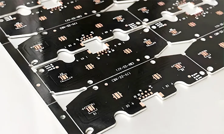
●Smooth Edge and Contour Precision: Methodical routing of board outlines and cutouts produces smooth edges, allowing for a perfect fit into mechanical enclosures, housings, and chassis.
●Void-Free Dielectric Bonding: Calibrated lamination processes produce a fully bonded dielectric interface without voids or resin-deficient zones. This solid structure supports efficient heat dissipation and helps prevent electrical failure throughout the product’s operational life.
Surface and Solder Mask Integrity
The surface of the PCB is the direct interface for components. Its preparation is a determining factor in the success of the soldering process and the long-term endurance of the assembly.
Appropriate Surface Finishes:
Finishes like Electroless Nickel Immersion Gold (ENIG) provide flat, solderable surfaces ideal for fine-pitch SMT components and can withstand the heat of reflow soldering. Organic Solderability Preservative (OSP) offers a cost-effective alternative when applied over a meticulously cleaned copper surface.
Durable Solder Mask Application:
Strong solder mask adhesion, achieved through proper surface preparation, prevents unintended solder bridging between components during assembly and protects the underlying copper from environmental corrosion.
Specialized Mask and Via Techniques:
In designs with high-power regions, selective coating and via plugging or tenting are employed to protect thermal pathways and ensure heat can be conducted away from components efficiently.
Quality Verification and Performance Validation
Verifying the quality of a VT-4B7SP board goes beyond a simple dimensional check. It involves a series of analyses to confirm its internal structure and its ability to withstand the stresses of assembly and operation.
Internal Structure Verification:
Cross-sectional analysis provides microscopic confirmation of correct layer alignment and complete resin coverage, ensuring the board’s internal construction matches the design specifications.
Assembly Stress Endurance:
Thermal shock and heat resistance testing verifies that the bonds between the aluminum, dielectric, and copper layers can endure the temperatures of multiple solder reflow cycles without degradation.
Electrical Conformance:
A combination of Automated Optical Inspection (AOI) and electrical testing ensures that trace spacing, pad positioning, and dielectric strength meet the design requirements across the entire production batch.
Section Highlights:
1.Fabrication Pillars: High-quality bare IMS boards rely on three pillars: precision mechanical processing, defect-free lamination bonding, and robust surface finishing.
2.Process Control: Every manufacturing detail, from hole cleanliness to solder mask adhesion, impacts final product performance and reliability.
3.Quality Validation: Multi-faceted verification through cross-sectioning, thermal shock tests, and electrical testing is required to ensure the bare board meets design specifications before delivery.
Advanced Fabrication Technologies for High-Density IMS
The theoretical benefits of a Ventec VT-4B7SP substrate are only realized through manufacturing technologies precise enough to handle its unique composite structure. Standard PCB fabrication techniques are often insufficient for meeting the tight tolerances and reliability demands of high-power automotive and industrial applications. Advanced fabrication capabilities are what separate a standard IMS board from a high-performance thermal management solution.
Precision Machining of Aluminum Substrates
The aluminum base of an IMS board presents unique machining challenges compared to standard FR-4. Overcoming these challenges is fundamental to the board’s mechanical fit and function.
Specialized Drilling and Tooling:
Standard HSS drill bits dull quickly against aluminum. The use of diamond-coated or solid carbide drill bits, combined with optimized feed and speed rates, is necessary to produce clean, burr-free holes without causing delamination. The use of proper entry and exit materials further guarantees hole quality.
Depth-Controlled Routing (Z-Axis Milling):
Many advanced designs require pockets, steps, or recesses to be milled into the aluminum base to accommodate component height or to create specific thermal contact zones. This requires high-precision Z-axis routing capabilities to control the depth of the cut to within microns, ensuring the dielectric layer is not compromised.
Laser Ablation and Cutting:
For creating very fine features or complex contours that are difficult to achieve with mechanical routing, laser cutting and ablation offer a non-contact alternative. This method can produce exceptionally smooth edges and can be used for selective removal of the dielectric material in highly specialized applications.
Lamination Process Control for Dielectric Integrity
The bond between the copper, dielectric, and aluminum is the heart of the IMS structure. A flawless bond is essential for both thermal transfer and high-voltage isolation.
Vacuum Lamination Press:
The lamination process must be performed in a vacuum press. This removes all air from between the layers before heat and pressure are applied, effectively eliminating the risk of voids or air pockets within the dielectric. Such voids can become points of electrical breakdown or severe thermal impedance.
Calibrated Thermal Profiling:
A precise, multi-stage thermal profile is used during the lamination cycle. The ramp-up rate, dwell time at peak temperature, and cool-down rate are all carefully controlled to ensure the dielectric resin flows and cures perfectly, achieving maximum bond strength without inducing internal stress in the material.
Surface Preparation Chemistry:
The chemical preparation of the copper and aluminum surfaces prior to lamination is a highly controlled process. Proper micro-etching of the surfaces creates a topography that promotes strong mechanical adhesion with the dielectric resin, guaranteeing resilience against delamination during thermal cycling.
Fine-Line Etching for Heavy Copper
High-power applications often require heavy copper weights (2oz, 3oz, or more). Etching thick copper while maintaining fine-line definitions for control circuitry is a significant challenge.
Differential and Spray Etching:
Standard immersion etching can result in significant “undercut,” where the etchant removes copper underneath the photoresist, leading to trapezoidal trace profiles and loss of line width control. Advanced spray etching systems with oscillating nozzles, combined with differential etching algorithms that adjust etch time for different areas of the board, are used to create straight sidewalls and precise trace geometries, even on heavy copper layers.
Automated Resist Stripping and Inspection:
After etching, the photoresist must be stripped completely without damaging the fine copper traces. Automated systems ensure consistent chemical exposure, while high-resolution AOI is used immediately after to verify that all traces and spaces meet the design specifications before the application of solder mask.
Section Highlights:
1.Advanced Machining: Specialized tooling, depth-controlled milling, and laser ablation are used to achieve complex physical shaping of the aluminum substrate.
2.Core Lamination Technique: Precision thermal pressing in a vacuum environment ensures a completely void-free dielectric, which is fundamental to high reliability.
3.Heavy Copper Etching: Advanced methods like differential etching solve the industry challenge of maintaining precise line definition on heavy copper layers.
Advanced Inspection and Testing Protocols for Zero-Defect IMS Boards
For high-reliability electronics, visual and basic electrical tests are insufficient. A zero-defect manufacturing philosophy for VT-4B7SP boards necessitates a suite of advanced inspection and testing protocols. These methods are designed to detect latent defects that could lead to field failures, providing the highest level of assurance for applications where performance and safety are non-negotiable. This rigorous approach to quality validation is a defining characteristic of a top-tier fabrication process.
High-Potential (Hi-Pot) and Insulation Resistance Testing
These tests directly assess the integrity of the dielectric layer, which is the most functionally significant feature of an IMS board.
Hi-Pot Testing Procedure:
This test applies a high DC or AC voltage (often several kilovolts) between the copper layer and the grounded aluminum base for a specified duration (e.g., 60 seconds). It is designed to detect any weaknesses in the dielectric, such as pinholes or areas of reduced thickness, that could lead to a catastrophic breakdown under operational voltage stress. A successful test shows minimal leakage current and no dielectric rupture.
Insulation Resistance (IR) Measurement:
Performed before and after Hi-Pot testing and thermal stress, the IR test measures the resistance of the dielectric layer, typically in gigaohms (GΩ) or teraohms (TΩ). A stable, high IR value confirms that the material’s insulating properties have not been degraded by manufacturing processes or environmental stress.
Impedance Verification with Time Domain Reflectometry (TDR)
While IMS boards are mainly used for thermal management, they are often part of systems that include high-speed digital communication. Maintaining controlled impedance is a requirement in these cases.
Integrated Test Coupons:
To verify impedance, special test traces (coupons) with the same geometry as the functional traces are designed into the production panel. These coupons are not part of the final board but experience the exact same manufacturing processes.
TDR Measurement:
A TDR instrument sends a high-speed pulse down the test coupon and analyzes the reflections. The shape of the reflected waveform allows for a precise calculation of the characteristic impedance along the entire trace length. This provides a quantitative guarantee that the final board will meet the signal integrity requirements of the design.
Ionic Contamination Testing
This advanced test quantifies residual ionic contaminants left on the board surface after chemical processes like etching and plating. It is a predictor of long-term reliability.
The Risk of Contamination:
Ionic residues (chlorides, sulfates, etc.), in the presence of humidity and electrical bias, can lead to a failure mechanism called electrochemical migration. This process causes the growth of metallic dendrites between conductors, eventually leading to a short circuit.
Ion Chromatography Method:
The test involves washing the board in a highly pure solvent solution and then analyzing the solution using ion chromatography. This technique separates and quantifies the specific ionic species present. The results are compared against established industry standards (e.g., IPC-TM-650) to ensure the board’s surface cleanliness meets the stringent requirements for long-term, high-reliability operation.
Accelerated Stress Testing (AST)
AST protocols simulate years of operational life in a matter of days or weeks, revealing potential wear-out mechanisms before a product reaches the field.
Thermal Shock Testing:
Boards are rapidly transferred between extreme temperature chambers (e.g., from -40°C to +125°C) for hundreds or thousands of cycles. This severe stress is designed to expose any weaknesses in solder joints, via plating, or material bonds.
Highly Accelerated Stress Test (HAST):
This test subjects the board to high temperature, high humidity, and pressure. HAST is particularly effective at accelerating failure mechanisms related to moisture ingress and corrosion, providing confidence in the board’s resilience in harsh environmental conditions.
Section Highlights:
1.Electrical Integrity Tests: High-Potential (Hi-Pot) testing and Insulation Resistance (IR) measurements verify the dielectric layer’s strength and durability.
2.Long-Term Reliability Verification: Ionic contamination and accelerated stress tests (thermal shock, HAST) uncover latent defects that could lead to future failures.
3.Beyond the Standard: A zero-defect outcome relies on an advanced testing framework that proactively finds and eliminates risks, going far beyond conventional checks.
Stack-up Design and Customization for Performance-Tuned Applications
The standard single-layer IMS construction of the Ventec VT-4B7SP provides a powerful foundation, but its true versatility is unlocked through customized stack-up configurations. Advanced fabrication capabilities enable the creation of tailored solutions that solve complex integration challenges, combining thermal management with dense signal routing and unique form factors. This level of customization moves beyond material selection and into the domain of integrated electronic system design.
Hybrid Stack-ups: Merging IMS and FR-4
For designs that require both a high-power section and a complex, multi-layered digital or RF section, a hybrid stack-up offers an elegant solution.
Construction Principle:
A hybrid board typically involves fabricating a standard multi-layer FR-4 board (containing the control and signal circuitry) and then laminating it to a VT-4B7SP substrate. Components in the high-power section are mounted on the IMS side, allowing direct heat transfer to the aluminum base, while fine-pitch digital components reside on the FR-4 side.
Fabrication Challenges:
This process requires expertise in dissimilar material lamination. Controlling warpage is a primary concern due to the significant CTE mismatch between FR-4 and aluminum. A precisely calibrated lamination cycle and a symmetric stack-up design are necessary to produce a flat and reliable final board. Interconnection between the FR-4 and IMS sections is achieved through carefully drilled and plated through-holes.
Hybrid Stack-up Design Table:
| Parameter | Typical Value / Range |
| FR-4 Layer Count | 2–8 layers (customizable) |
| IMS Substrate Material | Ventec VT-4B7SP |
| Lamination Cycle Temp. Range | 180–200°C |
| Lamination Pressure | 1.4–2.0 MPa |
| CTE Mismatch Management | Symmetrical stack-up design |
| Interconnection Method | PTH with selective backdrilling |
| Dielectric Isolation Requirement | > 3 kV |
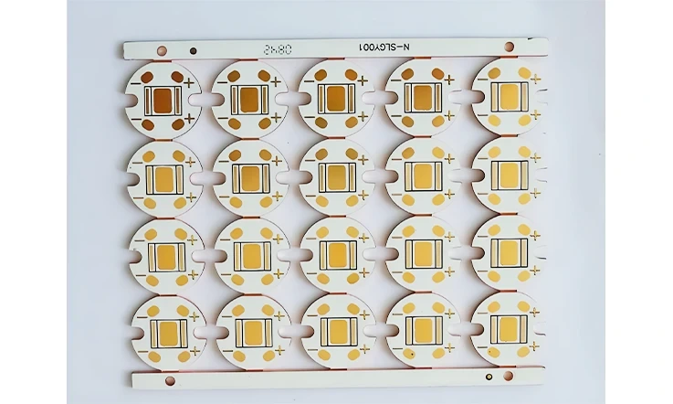
Double-Sided IMS Configurations
When component density requirements exceed the capacity of a single side, a double-sided IMS board can be developed. This doubles the available mounting area while retaining an excellent thermal pathway.
Structure:
A double-sided IMS board features a central aluminum core, with a dielectric layer and a copper circuit layer on both the top and bottom surfaces. This construction allows for SMT components to be mounted on both sides of the board.
Manufacturing Considerations:
The core challenge is maintaining electrical isolation. Each circuit layer must be fully insulated from the central aluminum core. The lamination process is more complex, requiring perfect alignment and bonding on both sides simultaneously. Thermal management must also be considered systemically, as heat from the bottom-side components must travel through the aluminum core to reach the primary heat sink, which is typically mounted to the top side.
Double-Sided IMS Stack Table:
| Parameter | Specification |
| Copper Thickness (Top/Bottom) | 1 oz – 4 oz per side |
| Aluminum Core Thickness | 1.0 mm – 2.0 mm |
| Dielectric Layer Thickness | 20 µm – 100 µm per side |
| Circuit Isolation Voltage | ≥ 4,000 V (both sides) |
| Lamination Process Type | Double-sided simultaneous |
| Max Board Thickness (typical) | 2.0 mm – 3.2 mm |
| Mounting Side | Dual (SMT on both layers) |
Balancing Dielectric Thickness and Copper Weight
The thermal performance of a VT-4B7SP board is directly tied to its thermal resistance (Rth).
Optimizing Thermal Impedance:
The thermal resistance of the dielectric is a function of its thickness and thermal conductivity. To minimize this resistance and improve heat transfer, a thinner dielectric is desirable. For instance, using a 20 µm dielectric instead of a 45 µm one can more than halve the thermal impedance. The resistance (Rth) can be expressed by dividing the material thickness (t) by the product of its thermal conductivity (k) and the area of heat transfer (A).
Engineering Trade-offs:
This choice involves a clear engineering trade-off. While a thinner dielectric improves thermal performance, it also results in a lower dielectric breakdown voltage and higher capacitance. Conversely, a thicker dielectric offers superior electrical isolation at the expense of thermal performance. Heavy copper weights can also influence the lamination process and must be factored into the overall design for manufacturability. A collaborative design process can help determine the optimal balance of these parameters for a specific application’s thermal and electrical budget.
Dielectric and Copper Balance Table:
| Parameter | 20 µm Dielectric | 45 µm Dielectric |
| Thermal Conductivity (k) | 7.0 W/m·K | 7.0 W/m·K |
| Thermal Resistance (Rth) | ~0.29 °C·cm²/W | ~0.64 °C·cm²/W |
| Breakdown Voltage | ~3,000 V | ~6,000 V |
| Dielectric Capacitance | Higher | Lower |
| Optimal Copper Weight | 1–2 oz | 2–4 oz |
| Suitable for Power Density | High | Moderate |
Section Highlights:
1.Beyond Standard Structures: Hybrid lamination of IMS with FR-4 is achievable for complex designs that integrate power and dense signaling.
2.Increased Integration Density: Double-sided IMS fabrication is supported, doubling component mounting area while maintaining an efficient thermal path.
3.Performance Tuning: Solutions can be performance-optimized for specific applications by precisely balancing dielectric thickness, copper weight, and thermal impedance.
Optimizing the Procurement Cycle: Cost, Quality, and Lead Time
For projects utilizing high-performance IMS substrates like Ventec VT-4B7SP, the procurement process extends far beyond a simple price comparison. A sophisticated approach is needed to balance the interconnected variables of manufacturing cost, unwavering quality, and predictable lead times. Understanding the drivers behind these factors empowers informed decision-making and fosters successful project outcomes.
Cost Structure Analysis for IMS Fabrication
The final cost of a VT-4B7SP board is a composite of material inputs and complex manufacturing processes. A transparent view of these cost drivers allows for effective design-to-cost optimization.
●Raw Material Influence: The primary cost is the substrate itself, influenced by the specified aluminum base thickness, dielectric thickness, and copper weight. Thicker aluminum and heavier copper (2oz or more) increase material expense but may be necessary for structural or thermal demands.
●Processing Complexity: Intricate routing, a high hole count, the need for depth-controlled drilling, and tight tolerances all increase machine time and engineering effort, thereby influencing the final price.
●Surface Finish Selection: The choice of surface finish has a direct cost implication. OSP is the most economical, while ENIG offers a balance of performance and cost. ENEPIG, with its additional palladium layer, represents a premium option for applications demanding the highest level of reliability.
●Panelization Efficiency: How individual boards are arranged on a master production panel greatly affects material utilization. An optimized panel layout minimizes waste and can substantially reduce the per-unit cost, especially in high-volume runs.
A Framework for Uncompromised Quality
Quality in IMS fabrication is not an inspection step; it is a system-wide discipline embedded in every process. It ensures that the board’s performance matches its design intent.
●Statistical Process Control (SPC): SPC is applied to processes such as etching and lamination to enable real-time tracking and adjustment. Through analysis of process data, variations can be addressed promptly to prevent defects, supporting dimensional accuracy and stable electrical characteristics throughout the production run.
●Advanced AOI and AVI: Automated Optical Inspection (AOI) systems for IMS are calibrated to account for the substrate’s unique reflective properties. They are followed by Automated Visual Inspection (AVI) to verify cosmetic standards and confirm features that AOI may not catch, such as solder mask uniformity.
●Robust Quality Management System (QMS): Adherence to rigorous QMS standards, such as IATF 16949 for the automotive sector, signifies a commitment to process control, risk management, and continuous improvement. This framework governs everything from raw material acceptance to final inspection and dispatch.
Achieving Predictable Lead Times
In today’s competitive landscape, time-to-market is a powerful advantage. Predictable and streamlined lead times are the result of operational excellence, not rushed work.
●Dedicated Production Lines: Allocating specific production lines or equipment cells for IMS materials minimizes setup time and cross-contamination. This allows for smoother workflow and faster throughput compared to general-purpose fabrication lines.
●Strategic Material Inventory: Maintaining a strategic inventory of common VT-4B7SP configurations (e.g., specific dielectric and aluminum thicknesses) can dramatically shorten lead times by eliminating delays associated with material sourcing from the supplier.
●Efficient CAM Engineering: The front-end engineering stage, where design data is translated into machine instructions (CAM), can be a bottleneck. A highly efficient CAM department with experience in IMS designs can quickly optimize panelization and generate tool paths, accelerating the project’s entry into the fabrication cycle.
Section Highlights:
1.Cost Transparency: Costs are driven by material selection, processing complexity, and panelization efficiency; a clear cost structure aids in design optimization.
2.Systemized Quality: Superior quality stems from a robust QMS, Statistical Process Control (SPC), and advanced automated inspection, not just final testing.
3.Punctual Delivery: Stable lead times depend on dedicated production lines, strategic material inventory, and efficient CAM engineering.
The Service Model for Complex IMS Projects
Delivering a high-performance IMS assembly built on Ventec VT-4B7SP involves more than just executing a fabrication order. It requires a comprehensive service model that supports the project from initial design through to final delivery. This model is characterized by proactive technical engagement, transparent communication, and robust logistical support, ensuring that complex designs are manufacturable, reliable, and delivered on schedule.
Proactive Design for Manufacturability (DFM) Feedback
An effective DFM review is a collaborative process that identifies and resolves potential manufacturing issues before they impact cost or lead time.
●IMS-Specific Analysis: DFM analysis for aluminum-backed boards goes beyond standard checks. It includes reviewing copper balancing to prevent warpage, assessing thermal via placement for optimal heat spreading, and verifying clearances around mechanically drilled features to ensure electrical integrity.
●Component Footprint and Land Pattern Verification:The service involves reviewing proposed land patterns based on IPC guidelines and practical manufacturing limits. This helps achieve the desired solder fillet shape, which supports the mechanical robustness and sustained performance of solder joints when exposed to thermal and mechanical stress.
●Panelization and Depaneling Strategy: An optimal depaneling strategy is proposed during the DFM stage. For IMS boards, V-scoring must be done with precise depth control to avoid cracking the dielectric. Tab routing with perforations is often a better alternative to minimize stress on the board and mounted components during separation.
Material Sourcing and Supply Chain Management
The availability of specialized materials like VT-4B7SP can be a project risk. A mature service model includes robust supply chain management to mitigate this.
●Qualified Material Sourcing: A verified supply chain ensures that all VT-4B7SP laminates are sourced directly from the material producer or their authorized distributors. This guarantees material authenticity and access to the latest product revisions.
●Inventory and Logistics: For recurring orders, a service can include holding a buffer stock of customer-specified laminate configurations. This decouples the project lead time from the material supplier’s lead time, enabling faster turnarounds and providing supply chain stability.
●Climate-Controlled Storage: All high-performance laminates are stored in a climate-controlled environment with strict monitoring of temperature and humidity. This preserves the material’s properties and ensures it performs as expected during the lamination and assembly processes.
Comprehensive Documentation and Traceability
For core applications in sectors like automotive, medical, or aerospace, complete traceability and documentation are non-negotiable.
●Full Material Traceability: The service provides complete lot-level traceability for all constituent materials, including the base laminate, copper foil, and even the solder mask and surface finish chemistry. Each board can be traced back to the specific material batches used in its construction.
●Quality Data Package: Upon request, a comprehensive data package can be supplied with the finished boards. This can include certificates of conformity, cross-section reports with photographic evidence, Time Domain Reflectometry (TDR) test results for impedance-controlled boards, and a detailed final inspection report summarizing all dimensional and electrical test results.
●Serialization: For the highest level of traceability, each individual board can be laser-marked with a unique serial number. This allows for tracking of a single unit throughout its assembly process and operational life.
Section Highlights:
1.Upfront Value: Professional DFM analysis is provided before fabrication begins, preventing design flaws at the source to save time and cost.
2.Supply Chain Assurance: Stable material supply and punctual project delivery are ensured through qualified sourcing and strategic inventory management.
3.Complete Traceability: Full documentation, from raw materials to final quality data packages, is available to meet the strictest industry requirements.
Proven Applications in Demanding Industries
The Ventec VT-4B7SP substrate has been validated across various high-demand sectors where heat dissipation, current density, and long-term endurance are primary design challenges. Its combination of a ceramic-filled dielectric and a high-conductivity aluminum base provides tangible performance advantages in real-world applications. The following sections highlight how this material enables superior design and performance in several industries.
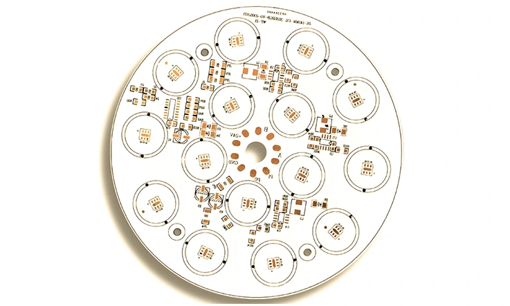
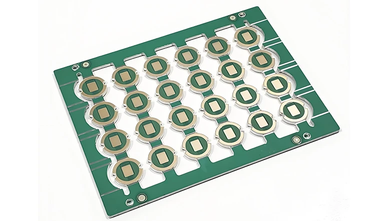
Automotive LED Lighting and Control Modules
In applications such as daytime running lights, matrix headlights, and advanced driver-assistance systems (ADAS), circuit boards must manage intense heat within compact, sealed enclosures.
●Enables High-Density Designs: The material’s properties support layouts with fine-pitch copper features and tight clearances, enabling the integration of complex control ICs and high-power LEDs into smaller modules.
●Withstands Thermal Stress of Assembly: The substrate endures the thermal demands of multiple solder reflow cycles, a common requirement for boards populated with high-power white LEDs whose junction temperatures affect light output.
●Maintains Precise Form Factor: The board’s structural integrity allows for intricate outlines and high-precision edges, a requirement for fitting into the complex carriers and housings of modern headlamp assemblies.
Industrial Motor Controllers and Inverters
Motor drives, servo systems, and power inverters for factory automation impose heavy thermal cycling and mechanical vibration on their circuit boards.
●Reduces Thermo-Mechanical Stress: The low Z-axis expansion of the ceramic-filled dielectric lessens stress on solder joints during high-temperature assembly processes and in operational use, enhancing the endurance of the completed assembly.
●Strengthens Bond in High-Vibration Environments: The robust bond between the copper and aluminum layers resists delamination, making it well-suited for industrial floor systems where mechanical shock and vibration are common.
●Supports Complex Power Topologies: The material allows for the creation of boards with high-integrity vias through thick copper layers, which is necessary for complex half-bridge and gate driver layouts rated for over 600 VDC.
Commercial and Architectural LED Lighting
The lifespan and lumen maintenance of commercial lighting, from street luminaires to high-bay fixtures, are directly linked to effective thermal management and dielectric durability.
●Improves Lumen Maintenance: The substrate’s high thermal conductivity efficiently draws heat away from LED packages. This helps maintain higher light output over a longer period, a reliable performance indicator for commercial lighting products.
●Facilitates Flawless SMT Assembly: The laminate surface is highly compatible with ENIG and OSP finishes, promoting strong solder mask adhesion and minimizing the risk of assembly defects like voids under large thermal pads.
●Ensures Optical Precision: The material’s resistance to warpage during processing results in a flat final board. This ensures all LEDs are mounted on a single plane, which is fundamental for achieving the intended optical distribution in wide-beam fixtures.
Section Highlights:
1.Automotive Electronics: In compact, high-temperature automotive modules, VT-4B7SP enables high-density layouts and reliable heat dissipation.
2.Industrial Control: Its robust structure withstands the vibration and thermal cycling of industrial environments, ensuring long-term stability for devices like motor drives.
3.Commercial Lighting: Efficient thermal performance helps extend LED life and maintain lumen output, enhancing the competitiveness of high-end lighting products.
Case Studies: From Engineering Challenges to Proven Solutions
Theoretical capabilities are best understood through real-world application. The following anonymized case studies illustrate how a combination of Ventec VT-4B7SP material and advanced fabrication expertise can solve complex engineering problems and deliver tangible results.
Case Study 1: Automotive Adaptive Matrix Headlamp
●The Challenge: A Tier-1 automotive supplier for a premium German brand was tasked with developing a next-generation adaptive headlamp. The primary objective was to double the number of addressable LED pixels from 64 to 128 within the existing module housing. This created a projected 40% increase in thermal load, placing the LEDs at high risk of exceeding their maximum allowable junction temperature and failing reliability targets.
●The Engineered Solution: A multi-faceted engineering approach was adopted.
1.A custom VT-4B7SP board with a thin 25 µm dielectric layer was specified to minimize thermal impedance between the LEDs and the aluminum base.
2.A 3oz heavy copper layer was used for the main power distribution plane, not only to handle the increased current but also to facilitate rapid lateral heat spreading away from the dense LED array.
3.Precision depth-controlled milling was employed to create shallow cavities on the aluminum base, allowing bulky driver ASICs to sit lower and maintain overall module planarity.
4.A collaborative DFM review led to the optimization of the thermal via array, with micro-vias placed directly under the thermal pad of each of the 128 LEDs, creating highly efficient, direct thermal pathways.
●The Result: The final assembly demonstrated a 20°C reduction in the peak LED junction temperature compared to the initial prototype built on a standard IMS board. The module successfully passed 1,500 hours of strenuous thermal shock testing (from -40°C to +125°C) with no measurable degradation in light output or electrical performance. This enabled the client to meet their ambitious power density targets and secure the high-volume production contract for the new vehicle platform.
Case Study 2: Industrial Robotic Arm Servo Drive
●The Challenge: A manufacturer of high-precision robotic arms for factory automation was experiencing premature field failures in their servo motor drives. Root cause analysis revealed that the existing FR-4 boards, which used thermal vias for heat dissipation, were susceptible to solder joint fatigue. The failures were caused by a combination of intense, high-frequency vibration and rapid thermal cycling during the robot’s acceleration and deceleration phases.
●The Engineered Solution: The design was completely migrated from FR-4 to a robust, single-layer VT-4B7SP substrate.
1.The monolithic IMS construction eliminated the internal CTE (Coefficient of Thermal Expansion) mismatches present in the previous multi-layer FR-4 design, which were a primary driver of solder joint stress.
2.The inherent rigidity of the thick aluminum base provided superior mechanical stability, effectively dampening vibrations transmitted from the motor assembly.
3.The high CTI value (>600V) of the VT-4B7SP material provided a significantly enhanced safety margin against electrical arcing, a concern in the potentially dusty factory environment.
4.An ENEPIG (Electroless Nickel Electroless Palladium Immersion Gold) surface finish was selected for its superior solder joint strength and resilience to vibration-induced fatigue.
●The Result: Field trial data from the new VT-4B7SP-based motor drives showed a 95% reduction in vibration-related electronic failures. The calculated Mean Time Between Failures (MTBF) for the drive electronics increased by an order of magnitude. The dramatic improvement in reliability allowed the robot manufacturer to offer a market-leading extended warranty, creating a powerful competitive advantage.
Why JarnisTech is the Premier Choice for Your Ventec VT-4B7SP Project?
You have read the guide. You understand the complexities and the potential of high-performance IMS technology. The final step is choosing a fabrication house that can transform this potential into a physical reality. At JarnisTech, we are not just another PCB supplier; we are specialists in high-performance thermal substrates, and we have built our reputation on turning our clients’ most demanding designs into successful products.
Mastering Advanced Fabrication Technology
The advanced processes detailed in this guide—from depth-controlled milling and vacuum lamination to heavy copper etching—are not just theoretical concepts at JarnisTech; they are part of our daily operations. Our facility is equipped with dedicated production lines optimized for IMS materials like the Ventec VT-4B7SP, ensuring a level of precision and repeatability that general-purpose fabricators cannot match. We have a deep, institutional understanding of how to handle these materials to maximize their performance.
Achieving Cost-Effectiveness Through Excellence
We deliver competitive pricing by eliminating inefficiency, not by compromising on quality. Through strategic material sourcing directly with Ventec and their authorized distributors, intelligent panelization that maximizes material usage, and a high-yield manufacturing process, JarnisTech minimizes waste. These savings are passed on to you, ensuring you receive a superior product at a fair and sustainable price. Our quotes are transparent, and our goal is to provide the best total value for your investment.
Unwavering Commitment to On-Time Delivery
In today’s market, meeting deadlines is non-negotiable. JarnisTech’s robust production planning, proactive supply chain management, and strategic inventory of core VT-4B7SP materials mean we can offer reliable and predictable lead times you can count on. We provide transparent scheduling from the moment you place your order to the day it ships, so you can manage your project timelines with confidence.
A True Partnership in Engineering Service
At JarnisTech, we believe fabrication is a service, not just a product. Our engagement begins long before your board hits the production floor. Our team of experienced DFM engineers becomes an extension of your own, providing a complimentary, in-depth analysis to optimize your design for reliability, performance, and cost. We are accessible, responsive, and fully invested in the success of your project from start to finish.
Realizing Performance: Your Path from Design to Final Assembly
The Ventec VT-4B7SP substrate provides the potential for exceptional thermal and electrical performance. This potential is unlocked when superior material properties are combined with expert design principles and a precision fabrication process from a dedicated specialist like JarnisTech.
Begin Your Project Feasibility Review
Your high-performance project deserves more than just a quote; it deserves a strategic, technical evaluation. Engaging with an experienced engineering group early in the design cycle is the most effective way to leverage the full capabilities of advanced IMS materials and ensure your design is optimized for both performance and manufacturability. Contact JarnisTech to submit your design for a complimentary feasibility review. Allow our engineering group to demonstrate how the potential of materials like Ventec VT-4B7SP is transformed into a flawless finished assembly that meets your most demanding performance goals.
FAQ about Ventec VT-4B7SP PCBs
Q: How is finished board bow and twist controlled and measured for VT-4B7SP, especially with heavy copper?
A: Control measures include symmetrical stack-up design, optimized lamination press cycles, and post-bake stress relief treatments. Measurement is performed using a granite surface plate and digital gauges to ensure compliance with IPC-A-600 Class 2 or higher standards.
Q: What is the typical shelf life of a finished VT-4B7SP PCB before assembly?
A: The shelf life primarily depends on the surface finish. For Electroless Nickel/Immersion Gold (ENIG), the shelf life is typically up to 12 months. For Organic Solderability Preservative (OSP), it is shorter, generally around 6 months.
Q: Can controlled impedance traces be fabricated on VT-4B7SP, and how is this verified?
A: Yes. Verification is performed by including impedance test coupons on every production panel. These coupons are then measured using a Time-Domain Reflectometer (TDR) to ensure the final trace geometry meets the specified impedance target (e.g., 50Ω).
Q: What are the primary factors that influence the lead time for a VT-4B7SP project?
A: Lead time is mainly driven by three factors: raw material availability and procurement cycle, the extended multi-stage lamination and curing time specific to IMS, and any additional complex machining or special testing requirements.
Q: How does design complexity, such as heavy copper or intricate outlines, affect the delivery schedule?
A: Heavy copper weights (>3oz) require longer plating and etching cycles. Intricate routed outlines require more CNC machine time compared to simple rectangular boards. Both of these factors can add several business days to the standard lead time.
Q: Is it possible to expedite an order for VT-4B7SP PCBs?
A: Expedited service can be available, depending on current material stock and production capacity. The multi-stage lamination and curing process has a minimum time requirement that cannot be compressed, but other steps in the workflow can often be accelerated to shorten the overall lead time.


