
Single sided aluminum PCBs are engineered to meet the demands of thermal regulation, electrical stability, and cost-conscious design within LED lighting and power conversion systems. Across diverse applications—ranging from high-lumen LED arrays to compact automotive lighting modules—these substrates integrate aluminum cores, optimized dielectric interfaces, and thermally balanced copper paths to support reliable system behavior under elevated loads.
This technical guide explores detailed design rules for trace and pad layout, surface-mounted LED component integration, and simulation-driven thermal analysis. It also covers fabrication capabilities such as CNC routing, V-cutting, and high-precision SMT placement, followed by inspection protocols including AOI, flying probe, and thermal shock testing. Additionally, we compare one-layer and dual-layer aluminum PCB structures, identify cost-impacting factors like copper thickness and production volume, and offer a step-by-step overview of how to submit project files for quotation and feedback.
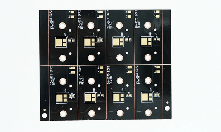
What is a Single Sided Aluminum PCB?
Single Sided Aluminum PCBs, also known as single-layer aluminum circuit boards, are widely used in thermal-sensitive electronic systems. These boards consist of a copper conductive layer, a thermally conductive dielectric, and an aluminum substrate. The design is structured to efficiently dissipate heat generated by electronic components without the need for complex cooling mechanisms.
This PCB type is commonly used in systems requiring stable thermal performance and mechanical durability. Industries such as LED lighting, automotive electronics, and industrial power control often specify single-sided aluminum boards to meet design and operational requirements. Their simple construction also contributes to cost-effective fabrication and streamlined assembly processes.
Basic Structure and Function of Single Layer MCPCBs
The basic design of a single-sided aluminum PCB includes a top copper layer for signal routing, a middle dielectric layer for thermal transfer and insulation, and a base aluminum layer that serves as the heat conductor. This straightforward configuration allows heat generated by active components to be channeled through the dielectric and into the aluminum substrate, where it disperses away from the core areas of the circuit.
●Copper Circuit Layer – Functions as the conductive trace path, allowing electrical current to travel between mounted components with high stability and low resistance.
●Thermally Conductive Dielectric – Acts as an insulating layer while also transferring heat from the copper traces to the aluminum base. Its thermal conductivity and thickness directly affect performance.
●Aluminum Substrate – Provides structural support and serves as the primary heat sink, efficiently dispersing thermal energy into the surrounding environment.
The thermal conductivity of the dielectric material is a main design parameter. Choosing an appropriate dielectric thickness and material affects the board’s heat transfer efficiency. The use of aluminum as the base material provides both mechanical strength and thermal efficiency, supporting reliable operation in various applications.
Advantages in Thermal Management for Power LED Circuits
In LED lighting setups, managing temperature conditions influences both output characteristics and product lifespan. Single Sided Aluminum PCBs promote even thermal flow across the board area, avoiding areas of concentrated heat. This allows LEDs to operate over longer durations at their intended luminous levels, while minimizing wear from elevated temperatures.
●Stable Heat Conduction – The aluminum layer allows for consistent and directional heat flow, preventing temperature buildup under high-power LED components.
●Material Optimization – The combination of dielectric and base materials enhances heat transfer without increasing the board’s thickness or mass.
●Enhanced Operational Lifespan – By maintaining manageable thermal levels, component stress is reduced, leading to improved longevity of LED assemblies.
By eliminating the need for additional heat-dissipating structures, these PCBs simplify mechanical design and improve the overall thermal profile of the system. As a result, LED drivers, lighting panels, and similar power electronic applications often implement this PCB structure to enhance thermal consistency.
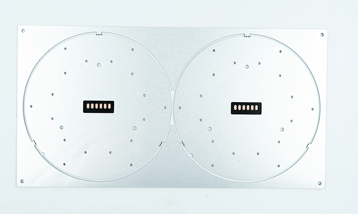
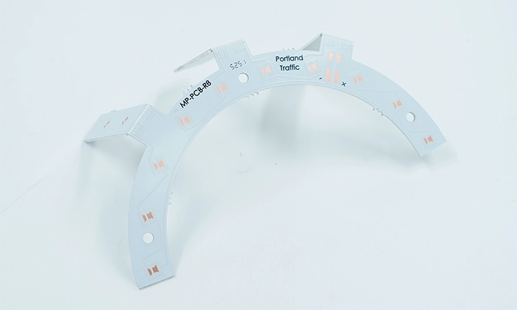
Applications in LED Modules, Automotive Lighting, and Power Systems
These PCBs are implemented across various sectors due to their thermal behavior and mechanical resilience. In LED modules, they enable compact layouts without the risk of overheating. In the automotive sector, single-sided aluminum boards support lighting systems that must operate under fluctuating temperatures and extended usage periods. Within industrial power electronics, they provide thermal control in high-current and high-frequency circuits, helping maintain operational stability under continuous load conditions.
●LED Modules – Used extensively in lighting panels, residential LED drivers, and architectural luminaires due to their thermal regulation and simple integration.
●Automotive Lighting – Used in daytime running lights, brake lights, and fog lamps, where stable heat behavior and strong resistance to mechanical stress are needed.
●Industrial Power Systems – Supports switching power supplies, control units, and inverter boards, which often operate in enclosed or high-load environments.
Their effectiveness in transferring heat away from sensitive components makes them suitable for use in environments where space, performance, and cost are closely managed. These characteristics continue to support their adoption in both consumer and professional-grade systems.
How Single Sided Aluminum PCBs Improve LED Reliability
When dealing with LED applications, managing heat dissipation and electrical performance through the circuit board design impacts long-term operation. Single sided aluminum PCBs serve as a practical solution by offering enhanced thermal paths and structural stability, which help reduce common failure modes in LEDs. The balance between insulating electrical paths and conducting heat away from components forms the foundation of durability in these boards. The following sections dive into how heat management, electrical insulation, and handling of voltage and current affect overall LED reliability.
Managing Heat to Extend LED Lifespan
The operational temperature of LEDs directly influences their degradation rate and output efficiency. Single sided aluminum PCBs deliver improved heat conduction through their metal core, channeling heat away from LEDs and reducing thermal buildup. This helps maintain junction temperatures within acceptable limits.
●Thermal conductivity of aluminum substrates typically ranges between 1.0–9.0 W/m·K, aiding heat dissipation.
●Copper layer thickness (commonly 35–70 µm) helps spread heat laterally across the board surface.
●The dielectric layer thickness and composition control thermal resistance and insulation, impacting overall heat transfer.
Table 1: Thermal Parameters of Single Sided Aluminum PCBs
| Parameter | Typical Value | Notes |
| Aluminum Thermal Conductivity | 1.0–9.0 W/m·K | Higher values offer better dissipation |
| Copper Thickness | 35–70 µm | Affects surface-level heat spreading |
| Dielectric Thickness | 75–150 µm | Adjusts vertical heat resistance |
| Dielectric Thermal Resistance | 0.3–0.8 W/m·K | Tradeoff between insulation and heat flow |
Efficient thermal management extends the LED lifespan by mitigating risks of overheating and thermal fatigue. Adjustments in layer thickness and material choice can tailor heat paths to specific LED power levels.
Electrical Insulation vs Thermal Conductivity Balance
Designing single sided aluminum PCBs involves maintaining a balance between electrical isolation and thermal transfer efficiency. The dielectric layer separates the conductive copper from the aluminum base, preventing electrical shorts while facilitating heat flow.
●Dielectric materials used generally exhibit thermal resistance between 0.3–0.8 W/m·K, balancing insulation needs and heat conduction.
●Selecting dielectrics with stable dielectric strength (20–40 kV/mm) ensures reliable electrical performance under operating voltages.
●PCB thickness and dielectric uniformity influence both mechanical stability and thermal behavior.
Table 2: Electrical and Thermal Characteristics of Dielectric Layers
| Dielectric Property | Range | Function |
| Dielectric Strength | 20–40 kV/mm | Prevents arcing, ensures insulation |
| Thermal Conductivity | 0.3–0.8 W/m·K | Facilitates heat transfer |
| Volume Resistivity | >10¹³ Ω·cm | Ensures electrical isolation |
| Breakdown Voltage | 2.5–4.5 kV | Threshold before insulation failure |
Optimizing these parameters ensures the board handles operational voltages safely without sacrificing heat management, which helps maintain LED function across various environments.
High Voltage and Current Handling in Aluminum Base PCBs
Single sided aluminum PCBs are designed to accommodate moderate to high currents typical in LED lighting circuits, while the aluminum base supports mechanical and thermal demands.
●Copper traces sized to accommodate currents up to several amperes prevent excessive voltage drop and resistive heating.
●Substrate and dielectric materials are chosen to tolerate voltages ranging from 12V up to 48V or more, common in LED modules.
●Proper trace width, pad sizing, and via placement reduce risks of electrical failure and hot spots on the board.
Table 3: Electrical Load Capabilities in Single Layer Aluminum Boards
| Parameter | Typical Range | Design Consideration |
| Trace Current Capacity | 1–10 A | Varies with copper thickness/width |
| Operating Voltage | 12V–48V+ | Common in LED and automotive uses |
| Minimum Trace Width | 0.3–1.5 mm | Prevents overheating and loss |
| Via/Pad Temperature Rise | <30°C | Ensures safe long-term operation |
This setup benefits LED lighting systems that operate under continuous current without early breakdowns. Ensuring both electrical handling and heat behavior are properly addressed increases the device’s durability.
Comparing Single Sided Aluminum PCB vs Double Layer MCPCB
In the manufacturing and design of metal core printed circuit boards (MCPCBs), deciding between single sided aluminum boards and double layer configurations influences several project parameters, including fabrication complexity, thermal management, and budget considerations. These two options deliver distinct approaches to electrical routing, heat conduction, and mechanical assembly, which impact their suitability across different electronic applications. By breaking down stack-up differences, application suitability, and performance thresholds, the following sections provide a thorough understanding to guide optimal PCB selection.
Differences in Stack-Up, Complexity, and Cost
Single sided aluminum PCBs consist of a straightforward stack-up—typically a copper circuit layer on top of a dielectric substrate bonded to an aluminum base. This simplicity results in fewer manufacturing steps and often reduces production time and expense.
●The single copper layer limits circuit routing options but streamlines fabrication flow.
●Double layer MCPCBs add another copper layer, separated by an additional insulating dielectric, increasing design flexibility but adding to board thickness and process steps.
●Increased layer count often corresponds with higher tooling and material costs, alongside extended turnaround times.
The tradeoff between simplicity and routing complexity translates directly into budget and project timeline decisions. Recognizing these tradeoffs helps ensure the fabrication process meets the intended performance and delivery goals.
Use Cases for Single vs Dual Layer Aluminum Boards
Choosing between single and double layer aluminum boards depends on the electrical and thermal demands of the target application. Single sided boards often meet the needs of LED lighting and power electronics where circuit paths remain relatively simple and heat dispersion is a primary consideration.
●Single layer boards suit applications where component density is moderate and heat transfer requirements dominate.
●Dual layer MCPCBs support designs with increased signal routing, allowing compact footprints and multi-functional circuits.
●They find applications in power amplifiers, motor controllers, and LED arrays with more intricate circuit arrangements.
Matching the board type to the electrical complexity and heat dissipation needs helps avoid overengineering or underperforming designs.
When to Select 1-Layer for LED vs High-Frequency RF Boards?
In the domain of LED applications, the preference for single sided aluminum PCBs stems from their capacity to channel heat away from diodes effectively while providing enough copper trace area for current flow. Their simpler stack-up reduces parasitic capacitance and inductance, factors that have minimal impact on LED lighting circuits.
●LED boards benefit from single sided designs as heat management takes precedence over complex signal routing.
●High-frequency RF circuits often require double sided or multi-layer boards due to their need for controlled impedance, shielding, and denser routing.
●Single layer aluminum boards typically don’t offer the precise electrical characteristics needed for RF signal integrity, especially above several GHz frequencies.
Choosing the right number of layers helps match electrical behavior to usage requirements while making practical use of production capabilities.
Core Materials in Single Sided Aluminum PCB Manufacturing
Single sided aluminum PCBs are constructed with a layered material system that must handle both electrical conductivity and thermal dispersion without compromising structural stability. The performance of these boards often comes down to precise control over base alloys, copper thickness, and the dielectric medium. Material selection in this context isn’t merely a matter of physical compatibility—it often determines how well the board performs under load, under heat, and over time.
Aluminum Substrate Types (5052, 6061, 1060 Alloys)
Before any copper is laminated or circuits are etched, the aluminum core forms the mechanical and thermal base of the PCB. The specific aluminum alloy used plays a measurable role in determining the board’s ability to handle repetitive thermal cycles, resist corrosion in humid or chemical environments, and support fine-tuned circuit routing.
●5052 Alloy – Selected where forming flexibility and corrosion behavior are relevant, particularly in sealed LED modules or sensor units subject to outdoor exposure.
●6061 Alloy – With greater tensile strength and machining compatibility, this alloy supports boards intended for structural mounting or where mechanical load-bearing may apply.
●1060 Alloy – Offers high thermal conductivity due to its purity, suitable for light engine arrays and driver modules that prioritize efficient heat dissipation over physical strength.
Understanding which alloy best fits a project’s goals helps reduce thermal stress concentration, minimize board deformation, and ensure predictable mounting performance.
Copper Foil Thickness and Thermal Dielectric Composition
The copper layer within a single sided aluminum PCB does more than route signals; it must also manage current density, temperature elevation, and connection reliability. Likewise, the dielectric material beneath this copper plays a supporting role in facilitating heat transfer, influencing both layout strategies and lifespan predictions.
●Copper Thickness – A thicker copper layer increases thermal mass and current-carrying capability, but it also demands careful trace width and spacing calculations to avoid excessive etching depth or delamination.
●Dielectric Composition – Dielectric layers typically consist of high-performance polymer composites filled with thermally conductive ceramics. Their performance is measured by thermal conductivity, breakdown voltage, and resistance to moisture ingress.
●Dielectric Thickness Control – Tight manufacturing tolerances on dielectric thickness (e.g., 75–150μm) influence thermal impedance, and selecting the right specification is typically based on watt density and product environment.
It’s recommended to select copper and dielectric combinations based on the unique needs of each circuit, rather than relying on default specifications—particularly in applications such as LED arrays or DC-DC converter platforms.
Comparison of FR4 vs Metal Core PCB Materials for Heat Dissipation
One of the earliest decisions in thermal-aware circuit design is selecting between traditional FR4 laminate and metal core substrates. While FR4 has been used across the PCB industry for decades, its thermal handling properties are inherently limited compared to aluminum-backed constructions.
●FR4 Material Overview – While widely used for multi-layer signal processing circuits, FR4’s thermal conductivity often limits its effectiveness in compact or enclosed LED housings or power modules.
●Metal Core Advantages – Aluminum-based PCBs provide direct thermal pathways for component heat, reducing the need for secondary heat sinks or complex via stitching. This leads to more predictable junction temperatures and simplified thermal simulations.
●Application Fit – In scenarios demanding structural strength, electromagnetic interference control, or compact layouts, aluminum substrates can maintain predictable performance without relying on added thermal pads or via-filling techniques.
This choice significantly affects not only thermal modeling but also stack-up design, final assembly processes, and cost structure.
Understanding Thermal Conductivity in Single Sided Aluminum PCB Design
Single sided aluminum PCBs are widely used in high-temperature electronics where maintaining consistent heat flow across the structure can influence electrical behavior. When these PCBs are deployed in systems like LED modules, automotive headlamps, and high-power converters, their ability to direct heat away from heat-generating elements becomes a central design consideration. This section delves into the structural properties and physical behavior of materials like dielectric layers and copper foils, and how simulation-based planning supports their implementation.
Dielectric Layer Thermal Resistance (W/m·K) and Its Practical Impact
The dielectric layer, sandwiched between the aluminum base and the conductive copper pattern, serves a dual purpose—maintaining electrical isolation and enabling directional heat transfer. Its thermal conductivity, measured in watts per meter-kelvin (W/m·K), is a controllable factor during material selection.
●Range of Material Options – Commonly used materials offer values between 1.0 W/m·K to over 9.0 W/m·K. Higher values generally reflect improved heat throughput across shorter paths.
●Effect of Thickness – A thinner layer typically reduces thermal resistance, allowing more heat to pass through in less time. However, too thin a layer may compromise dielectric integrity.
●Stability Under Load – Dielectric properties may shift under prolonged exposure to heat or operational stress. Choosing substrates that retain stable electrical behavior over time helps maintain functional reliability under demanding conditions.
Table 1: Dielectric Layer Parameters
| Parameter | Typical Values | Application Relevance |
| Thermal Conductivity | 1.0 – 9.0 W/m·K | Higher values improve vertical heat transfer |
| Thickness | 75 – 150 µm | Affects both thermal resistance and insulation |
| Dielectric Strength | 20 – 40 kV/mm | Prevents electrical shorts |
| Thermal Resistance | 0.3 – 0.8 °C·cm²/W | Key to efficient heat conduction |
Some Designers typically weigh these factors according to the intended use, cost constraints, and performance requirements.
Copper Clad Function in Thermal and Electrical Distribution
Copper, as the primary conductive path, also helps redistribute heat laterally across the surface before it travels downward through the dielectric layer. In single sided aluminum PCBs, copper thickness directly affects this horizontal dissipation and the volume of current the board can support.
●Thickness Options – Industry standard starts at 1 oz (35µm), with variations like 2 oz (70µm) or even 3 oz (105µm) used for systems carrying larger current.
●Thermal Impedance Considerations – Thicker copper can decrease localized temperature rise by distributing the heat more evenly across the board surface.
●Surface Finishing – Treatments like ENIG (Electroless Nickel Immersion Gold) or HASL (Hot Air Solder Leveling) affect thermal resistance at junctions with components and should be selected based on the assembly method.
Table 2: Copper Foil Characteristics
| Copper Weight | Thickness (µm) | Current Capacity (A) | Notes |
| 1 oz | 35 | ~2–4 | Standard for low–mid power designs |
| 2 oz | 70 | ~5–8 | For higher current or heat loads |
| 3 oz | 105 | ~8–12 | High-power lighting or converters |
| Surface Finish | — | — | ENIG = low oxidation, HASL = cost-effective |
By manipulating copper weight and pattern design, thermal behavior can be tuned without altering the physical thickness of the board.
Simulation and Analysis for Heat-Intensive Applications
Thermal modeling is frequently adopted during the design stage of single sided aluminum PCBs to simulate how temperature will distribute across the surface and through each material layer. These insights help refine placement, orientation, and component separation before a physical prototype is built.
●Pre-Layout Predictions – Simulation tools enable early forecasting of temperature rise around components, especially high-wattage drivers, MOSFETs, or LEDs.
●Material Behavior Comparison – Various aluminum alloys and dielectric combinations can be virtually tested to identify which match the intended dissipation path.
●Long-Term Planning – Some simulations allow for time-based thermal loading, which gives designers a window into how aging components will behave under real-world duty cycles.
Table 3: Thermal Simulation Considerations
| Simulation Factor | Function | Design Outcome |
| Max Operating Temp | Defines temperature limits for layout | Guides component clearance and copper paths |
| Junction Temp Forecast | Estimates LED or IC core temperatures | Helps avoid thermal runaway |
| Time-based Load Cycling | Simulates real-world duty cycles | Supports lifetime reliability calculations |
| Material Set Comparison | Analyzes heat spread of stackups | Aids material selection during prototyping |
Modeling also reduces the chances of post-production rework, streamlining the prototyping cycle and improving turnaround times for production-ready designs.
Custom Single Sided Aluminum PCB Design Guidelines
As PCB engineers and manufacturers in the aluminum-based board segment know, customizing layout and thermal handling for Single Sided Aluminum PCBs involves more than just choosing substrates and copper weight. It includes tuning every design dimension — from pad shapes to trace paths — to align with real thermal dissipation needs, electrical requirements, and assembly tolerances. The following subsections delve into layout tuning for LED modules and power applications, helping engineers align design precision with material characteristics and production repeatability.
Trace Width, Pad Size, and Via Guidelines for LED PCBs
In Single Sided Aluminum PCB layout, copper trace width and pad sizing define how a board handles electrical and thermal demands under continuous operation. Incorrect dimensioning not only affects current flow but may also create thermal stress points that shorten product lifespan or complicate manufacturing.
● Trace Width-
– Should be selected based on copper thickness and continuous current.
– Use IPC-2152 guidelines for baseline values, adjusting with safety margin based on ambient conditions.
– Wider traces support better thermal movement laterally across the copper plane.
● Pad Size and Geometry-
– Pads must ensure full contact with LED terminals or driver ICs.
– Rounded corners and anti-pad spacing should reflect the soldering method and heat flow pattern.
– Avoid sharp edges that might concentrate heat or stress.
● Via Design Considerations-
– Though Single Sided Aluminum PCBs typically do not include through-hole vias, plated slots or mechanical drill-outs may be introduced for grounding or mounting.
– These must be isolated carefully to avoid shorts between copper and aluminum core.
Designing for Surface Mount LED Components (SMD, COB)
Surface mount LEDs, whether in SMD or COB formats, require careful coordination between pad layout, solder mask opening, and heat transfer interface. Variations in these elements can lead to light fluctuation, thermal fatigue, or open joints during the reflow phase.
● Footprint Alignment-
– Ensure alignment with LED manufacturer land pattern recommendations.
– Allow sufficient pad size for complete solder wetting without creating solder bridges.
– Center pad (for thermal pad LEDs) should have 100% copper exposure for best thermal transmission.
● Solder Mask Strategy-
– For thermal pads, remove solder mask completely.
– Define solder mask dams only where needed to prevent solder overflow.
● Mounting Flatness-
– Check for copper surface flatness during fabrication.
– Avoid oxidation on exposed copper areas — even slight tarnishing increases thermal resistance.
PCB Layout Optimization for Uniform Heat Dissipation
Thermal performance in aluminum PCBs does not rely solely on material specs. Layout symmetry, component spacing, and copper pours greatly affect how heat is spread and released. Without appropriate routing, hotspots may form that compromise LED brightness or component reliability.
● Component Distribution-
– Spread heat-generating components evenly to avoid localized heat.
– Use simulation software to visualize surface temperature gradients.
● Copper Plane Design-
– Maximize the use of ground plane copper to extend thermal conduction areas.
– Connect all heat-producing pads to thermal pours without narrow neck-downs.
● Routing Considerations-
– Avoid routing sensitive traces near large copper pours without separation.
– Consider single-point grounding for better control over potential loops.
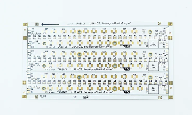
JarnisTech – Single Sided Aluminum PCB Manufacturing Capabilities
The fabrication of single sided aluminum PCBs relies on steady quality and precise processes to support lasting performance. At JarnisTech, production methods focus on practical manufacturing needs—accurate board contouring, heat-managed assembly, and uniform inspection routines. Each stage, from substrate preparation to component mounting and final verification, undergoes thorough oversight to fulfill the demands of thermal management designs used in lighting arrays, control systems, and high-wattage electronics.
Here’s a detailed look into how JarnisTech processes aluminum-based single layer PCBs for industrial applications:
CNC Drilling, Routing, and V-Cut for Precision Board Shaping
The shaping of metal-core boards begins with controlled mechanical processing designed to support mounting, integration, and modular assembly.
●CNC Drilling: Precision-guided drills are programmed to achieve uniform aperture size and depth, ensuring clean hole walls that aid component insertion and fixture alignment.
●Routing: Outer profiles and custom internal slots are milled to exact shapes, supporting compatibility with housing units or fixtures across various product lines.
●V-Cutting: When multiple boards are panelized, V-cuts provide breakaway points that maintain structural integrity during handling and allow for tool-free separation during final use.
This level of control over board geometry helps ensure structural compatibility with LED heat sinks, modular connectors, and aluminum panel housing.
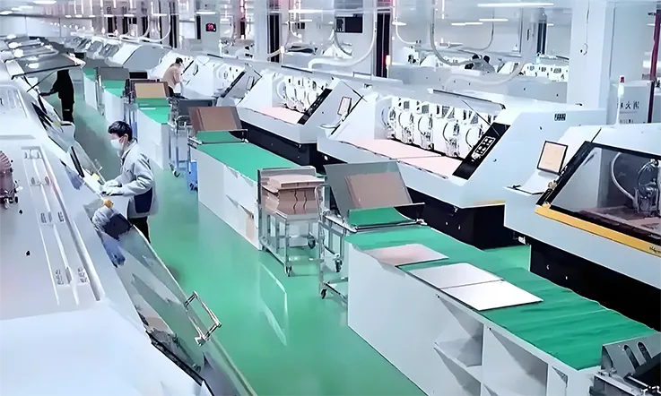
SMT Assembly and LED Chip Mounting for MCPCB Applications
Handling metal substrates during SMT production requires care in both thermal calibration and placement accuracy. At JarnisTech, this process is tuned for metal-core board behavior.
●Paste Printing: Solder paste is applied with stainless steel stencils over copper pads using volume-controlled printers, tuned to support high-output LED packages.
●Component Placement: LED chips and power parts are placed using steady feeders and precise optical positioning, limiting movement and decreasing shadow effects.
●Reflow Soldering: Thermal profiles are configured for aluminum-backed layers, avoiding stress to the dielectric or overexposure of LEDs.
This assembly flow is structured for LED modules, sensor control panels, and compact DC supply boards.
Testing Protocols: AOI, Flying Probe, and Thermal Shock
After assembly, each board undergoes validation to confirm both surface condition and electrical function under operational stress.
●AOI (Automated Optical Inspection): Optical systems scan surface pads, solder joints, and component positions, flagging bridging, lift, or skew.
●Flying Probe Electrical Testing: Non-invasive testing heads verify circuit continuity, connection integrity, and resistance thresholds without dedicated fixtures—supporting both prototypes and production runs.
●Thermal Shock Simulation: Metal-core samples are placed in variable chambers, exposing them to repeated thermal cycling to simulate field conditions in outdoor or high-output use cases.
Each test confirms the board is ready for function where thermal control, power density, and assembly integrity matter.
Why Choose Us as Your Single Sided Aluminum PCB Manufacturer?
Selecting a manufacturer in the field of single sided aluminum PCBs is more than just price-checking and lead-time comparisons. For industries like LED lighting, automotive signaling, and high-wattage power equipment, precision, compliance, and technical support can shape the entire product lifecycle. JarnisTech positions itself as a dependable production partner with advanced process integration, strong quality systems, and a global delivery footprint.
Certifications (ISO9001, UL, RoHS) and Mass Production Capability
Our compliance with major international standards is not just a checkbox — it’s a reflection of the structure we bring to our manufacturing environment.
●ISO 9001:2015 processes are applied across our full production line, from incoming raw materials to outgoing finished PCBs.
●UL-certified aluminum base materials ensure compatibility with lighting-grade safety norms.
●RoHS-compliant finishes are standard, especially for LED and consumer electronics industries.
JarnisTech’s production floor supports mid- to high-volume orders, and our aluminum MCPCB line maintains throughput for demanding timelines.
Design for Manufacturability Support and Rapid Prototyping Services
Prototypes and production-scale outputs are often separated by design gaps. We help close them early in the process through practical DFM guidance.
●PCB layout reviews address copper width, thermal paths, and material stackups before fab begins.
●1–3 day prototyping is available with express aluminum PCB turnaround on standard designs.
●All prototype-to-production transfers include matching aluminum substrate specs and copper foil standards.
This process reduces the chance of iterations post-pilot and supports a direct handoff to SMT assembly when needed.
Global Logistics and Export-Focused Manufacturing Support
Exporting aluminum-based MCPCBs presents a range of challenges — from documentation to temperature-controlled shipping. Our logistics team works closely with buyers to simplify the international handling process.
●Experienced with both EXW and DDP terms, and capable of shipping to over 112countries.
●All shipments are moisture-barrier packed with desiccant and vacuum-sealed to meet storage standards.
●Export-grade labels, compliance documents, and HS code support are included with every batch.
Therefore, whether the shipment heads to an LED fixture assembly line in Germany or a traffic signal module in Dubai, we’re ready to provide reliable delivery every time.
Single Layer MCPCB Cost Factors and Optimization Tips
Understanding the various elements that influence the expense of single layer metal core printed circuit boards (MCPCBs) provides a solid foundation for effective cost management. Pricing is driven by factors such as material choices, fabrication complexity, and order quantity. Evaluating how board dimensions, copper thickness, and layer count contribute to overall cost enables reliable design decisions. When combined with pricing structures that adjust according to production volume, as well as techniques for moving from prototype stages to full production, this knowledge supports balancing technical requirements with budget considerations.
How Board Size, Copper Weight, and Layers Affect Price?
●Board size determines the quantity of raw materials needed and the extent of fabrication processes, with larger boards resulting in increased costs.
●Copper weight impacts electrical and thermal properties, with heavier copper adding to material expenses but potentially reducing the need for costly revisions.
●While single-sided MCPCBs involve fewer layers, the dielectric thickness used for insulation and heat dissipation can affect processing steps and price.
| Parameter | Typical Range | Impact on Cost |
| Board Size | 50 mm² – 5000 mm² | Material and fabrication costs rise with size |
| Copper Weight | 1 oz – 5 oz | Heavier copper increases raw material cost and handling requirements |
| Layer Count | 1 Layer (Single Side) | Simpler processing generally lowers cost but thicker dielectrics may add complexity |
A clear understanding of these factors early in the design process can prevent unexpected expenses later.
Volume-Based Costing and Prototype-to-Production Scaling
●Low volume orders typically incur higher unit costs due to setup and handling fees that don’t scale down easily.
●Increasing order quantities allows fixed costs to distribute across more units, resulting in lower per-unit prices.
●Adjusting designs between prototype and full production phases may optimize fabrication efficiency, such as refining copper thickness or minimizing layer complexity to reduce costs.
| Production Volume | Estimated Cost per Unit | Notes |
| Prototype (10 pcs) | $50 – $70 | Setup and manual processes dominate cost |
| Small Batch (100 pcs) | $20 – $30 | Some volume discounts apply |
| Mass Production (1000+ pcs) | $8 – $15 | Automated fabrication and bulk pricing |
Clarifying production volume expectations early in the process supports realistic budgeting and scheduling.
Design-for-Cost (DFC) in High-Power LED Lighting Projects
●Optimizing trace widths and pad dimensions can reduce copper usage while maintaining reliable electrical performance.
●Selecting appropriate dielectric thickness balances heat conduction and electrical insulation without overspending on materials.
●Minimizing component complexity and via counts can shorten assembly time, impacting labor and handling expenses.
Applying these design strategies supports production goals while maintaining required performance and structural strength, particularly in demanding high-power lighting environments.
How to Request Your Custom Single Sided Aluminum PCB Quote Today?
Single Sided Aluminum Circuit Boards
Obtaining a precise single sided aluminum PCB manufacturing quote involves submitting detailed design files and specifications. Clear communication of requirements helps streamline the quoting process and reduces uncertainties. This section breaks down the main steps for requesting a quote, highlighting necessary documentation and expected interactions with the manufacturer.
Submit Gerber Files, BOM, and Custom Specs
The foundation for any manufacturing quote lies in the Gerber files, which provide exact layouts of copper traces, drill patterns, and solder masks. Including a comprehensive bill of materials (BOM) clarifies component types and quantities, influencing sourcing and assembly considerations. Custom specifications on substrate thickness, copper foil weight, and thermal properties guide material selection and process planning.
●Accurate file submission cuts down on unnecessary revisions.
●Detailed specifications enable precise cost and timeline estimation.
| Submission Item | Function | Impact on Quoting |
| Gerber Files | Defines circuit patterns and drill holes | Enables detailed fabrication planning |
| Bill of Materials | Lists components and quantities | Influences sourcing and assembly |
| Custom Specifications | Details on materials and thermal features | Shapes processing and cost analysis |
Response in 12 Hours from a Trusted China PCB Manufacturer
Manufacturers experienced in single sided aluminum PCB production often deliver initial quotes within 12 hours after receiving all required documents. This prompt feedback stems from structured processes and streamlined correspondence built around short lead-time requests. Quick replies assist with timeline coordination and cost forecasting.
●Quick replies help keep project schedules on track.
●Manufacturers with streamlined processes balance speed with thorough cost assessment.
| Response Type | Typical Timeframe | Benefit to Buyer |
| Initial Quotation | Within 12 hours | Enables rapid budget review |
| Follow-Up Clarifications | Within 24 hours | Keeps communication open |
| Detailed Design Review | Within 48 hours | Provides manufacturing insights |
Get Thermal and Electrical Design Feedback From Our Engineering Team
Design review processes focus on improving thermal dissipation and electrical performance of single sided aluminum PCBs. Feedback covers copper thickness, dielectric layer properties, and substrate materials, highlighting opportunities to optimize layout and material choices. This input helps minimize manufacturing challenges and supports long-term reliability.
●Early feedback identifies potential design adjustments.
●Experienced technical teams offer material and layout recommendations.
| Feedback Focus | Areas Considered | Possible Suggestions |
| Thermal Management | Heat transfer efficiency, layer resistances | Adjust dielectric thickness or copper patterns |
| Electrical Integrity | Trace widths, pad sizes | Modify trace geometry and spacing |
| Material Compatibility | Alloy selection, copper foil types | Suggest alternative materials |
Ready to take the next step? Send your Gerber files, BOM, and custom specs to jumpstart the process. We’ll get your quote rolling and offer design insights that keep your single sided aluminum PCB project moving along without a hitch. Don’t wait—reach out now and see how simple requesting a custom quote can be.
FAQs – Single Sided Aluminum PCBs
1.What is the typical thickness of the aluminum base in single sided PCBs?
Most aluminum base layers range from 1.0mm to 3.2mm, depending on mechanical strength and thermal performance requirements.
2.What is the max copper thickness that can be used?
Copper thickness typically ranges from 1oz to 4oz (35μm–140μm), but heavier copper can be used for high-current paths.
3.Can these PCBs be used in outdoor or high-humidity environments?
Yes, when combined with conformal coating or encapsulation, they can perform reliably in harsh conditions.
4.What dielectric layer thickness is standard?
Typically between 50μm and 150μm, depending on required insulation strength and heat transfer performance.
5.Is there a limit to the board size in single sided aluminum PCB manufacturing?
Most suppliers can fabricate panels up to 600mm x 1200mm, but larger sizes may incur warpage risks.
6.Can I request partial aluminum cutouts for thermal isolation?
Yes, partial routing or pocket milling is possible to isolate thermal zones or reduce weight.
7.How long is the typical lead time for production?
Standard lead time is around 7–10 working days for small to medium runs, depending on complexity.


