
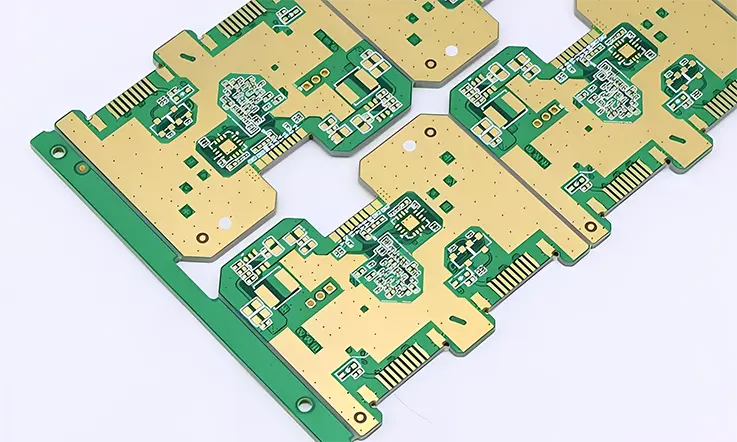
4 oz copper PCBs are widely applied in high-current and thermal management environments. These circuit boards are specifically tailored to support power-heavy systems, offering strong structural capacity for high-voltage circuitry and effective heat transfer. As electronic devices become more compact and power loads increase, consistent performance and long-term durability in PCB layouts are increasingly demanded—particularly across sectors like industrial automation, aerospace, automotive engineering, and LED technologies.
This guide explores the various aspects of 4 oz copper PCBs, from selecting the right materials to advanced manufacturing techniques. We will delve into the specifics of high-current capabilities, the strategies for managing thermal challenges, and how to implement effective PCB stackup configurations to prevent issues like delamination or warping. Additionally, we’ll cover design considerations such as trace width, via hole plating, and etch-back control to ensure maximum performance.
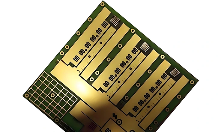
What Is a 4 oz Copper PCB?
Why It Matters in Power Electronics?
In power electronics, the physical structure of the PCB often determines whether a system can perform safely and reliably under sustained electrical stress. While the industry-standard 1 oz copper PCBs may be sufficient for small signal or low-power designs, they tend to struggle in high-current environments where copper thickness directly affects electrical and thermal performance.
A 4 oz copper PCB, by contrast, is engineered with thicker copper layers that can handle higher current loads and offer greater heat dissipation capacity. For sectors such as industrial automation, high-wattage LED lighting, automotive power modules, and energy distribution systems, selecting a thicker copper PCB enables more stable electrical behavior and reduces long-term maintenance needs.
The following sections explore what sets 4 oz copper PCBs apart from standard designs and how they provide practical solutions in demanding industrial applications.
Understanding Copper Thickness: From 1 oz to 4 oz
Copper thickness in PCB design is typically described in ounces per square foot. This unit refers to the weight of copper distributed evenly over a one-square-foot area. Each ounce corresponds to a copper layer thickness of approximately 35 microns. Therefore:
●1 oz = ~35 μm
●2 oz = ~70 μm
●3 oz = ~105 μm
●4 oz = ~140 μm
As copper thickness increases, so does the current-carrying capacity of the traces. This expansion provides multiple benefits: reduced conductor resistance, improved thermal performance, and increased mechanical stability. For engineers working with circuits where current exceeds 10A or where thermal regulation is difficult due to component density, heavier copper often becomes necessary.
Thicker copper also supports wider trace widths, reducing the risk of overheating during continuous operation. This consideration becomes especially useful in motor controllers, power converters, and high-output battery charging systems.
Benefits of 4 oz Copper in High Current Circuits
Designing high-current circuits comes with its own set of challenges. Heat buildup, voltage drops, and material fatigue are all serious risks that can cause failure in the field. A 4 oz copper PCB helps minimize these risks in several ways:
●Increased current capacity: Thicker copper traces can accommodate higher levels of current without experiencing elevated temperatures that degrade performance.
●Lower thermal resistance: Improved heat dissipation extends component lifespan and stabilizes operation under continuous load.
●Improved reliability: Higher copper mass strengthens the entire PCB structure, reducing issues caused by thermal expansion or vibration, especially in harsh operating environments.
For example, in an electric vehicle charging station designed to deliver over 40A to a battery system, a 1 oz PCB would require unreasonably wide traces and complex cooling solutions. A 4 oz PCB simplifies the layout and improves safety margins with no additional thermal interface materials.
Comparison with Standard PCBs for Industrial Devices
Standard PCBs, typically built with 1 oz copper, serve well in low-power systems such as communication devices or control panels with minimal current flow. However, when used in high-load systems, these boards are often pushed beyond their capability, leading to problems like overheating, trace deformation, and eventual failure.
By comparison, 4 oz copper PCBs provide a more robust and thermally stable platform. They are particularly well suited for:
●Industrial motor drives
●Power amplifiers
●Solar power inverters
●LED drivers with high forward current requirements
In environments where systems must operate continuously for thousands of hours or withstand frequent power surges, standard PCBs often degrade prematurely. Using a 4 oz copper PCB can reduce the risk of breakdowns and unplanned downtime by improving electrical and thermal headroom.
Core Applications of 4 oz Copper PCB in Industrial and LED Systems
When building electronics for industries that rely on consistent high-current handling and dependable thermal performance, selecting the right type of PCB is a strategic move. A 4 oz copper PCB, crafted with thicker copper layers, opens up new design opportunities for human facing challenges such as heat dissipation, current density management, and mechanical durability.
From LED lighting modules to heavy-duty industrial equipment, and even aerospace and automotive electronics, the application range of a 4 oz copper PCB continues to grow. Working with a skilled Heavy Copper PCB Manufacturer can help bridge the gap between conceptual design and real-world durability. Let’s dive into the sectors where these heavy copper boards have truly made a difference.
4 oz Copper PCB in LED Lighting Modules
LED lighting systems have shifted from niche applications to becoming the core of industrial and commercial infrastructure. In large-scale stadium lighting, high-bay industrial fixtures, and architectural illumination projects, LED modules must handle high forward currents while keeping thermal performance tightly controlled.
In LED driver circuits and COB (Chip-On-Board) assemblies, a 4 oz Copper PCB enables:
●Efficient heat distribution: Copper’s thermal conductivity ensures that excess heat moves quickly away from sensitive diodes.
●Higher current-carrying pathways: Especially for high-power LEDs that can draw significant amperage per array.
●Reduced risk of thermal runaway: By minimizing localized heating, the entire board remains safer over prolonged usage.
Take an example: A high-bay LED module designed for warehouse lighting typically runs at 150W or higher. In such designs, using a standard 1 oz copper PCB could lead to early degradation. A 4 oz copper PCB helps manage these thermal and current stresses far more efficiently, leading to longer operating life and greater lighting consistency.
High Amperage PCBs in Industrial Equipment
Industries running automation lines, CNC machinery, welding robots, or high-capacity pumps cannot afford breakdowns due to overheated PCBs. When current loads start pushing 50A, 100A, or beyond, traditional PCBs reach their practical limits quickly.
By deploying a 4 oz Copper PCB in industrial equipment, designers achieve:
●Thicker traces that handle aggressive current loads without requiring massive physical dimensions.
●Better resistance to mechanical stresses such as vibration and thermal cycling, common in factory environments.
●Simplified layout designs, since wider traces or multiple parallel paths become less necessary.
As an example, a motor control board operating at 400V and handling a 120A peak load for conveyor belt drives demands rugged PCB infrastructure. Without a 4 oz copper board, engineers would either have to significantly over-engineer the cooling system or accept shortened lifespan risks.
Aerospace & Automotive Systems Using Heavy Copper
Applications in aerospace and automotive electronics push PCBs to their physical and environmental limits. Systems must endure temperature extremes, fluctuating mechanical loads, and high continuous currents—all at once.
Areas where 4 oz copper PCBs shine include:
●Battery Management Systems (BMS): Electric vehicles require PCBs that can safely route substantial battery currents while minimizing voltage drops.
●Power Distribution Units (PDUs): These core modules need reliable copper pathways to handle the power demands of modern automotive features such as autonomous driving systems.
●Avionics Power Control Systems: Aircraft electronics need ruggedized PCBs that perform across wide temperature bands without failure.
For instance, in electric vehicle battery packs, the main power boards often experience surges up to 200A. A Heavy Copper PCB Manufacturer(Jarnistech) can produce custom solutions where conventional 1 oz or 2 oz PCBs would simply fall short.
Design Heavy Copper PCB Considerations for Engineers
When working with high-current circuits, our engineers often turn to 4 oz Copper PCBs to handle the electrical load while maintaining mechanical reliability and thermal consistency. The increased copper thickness opens up design opportunities, but it also brings new considerations in layout, stackup, spacing, and heat management.
Below, we’ll explore several essential aspects of designing with heavy copper, particularly for applications involving elevated current and voltage ranges.
Designing for High Current and Voltage
Managing current flow and voltage thresholds in high-power applications demands close attention to copper thickness, spacing, and board thermal behavior. A 4 oz Copper PCB provides ample conductivity, but effective design ensures that this potential is fully utilized without introducing thermal or electrical stress.
Key considerations:
Current-Carrying Requirements-
Each ounce of copper provides approximately 35µm of thickness. In a 4 oz Copper PCB, traces are roughly 140µm thick, supporting higher current loads—often between 50A to 150A—depending on trace width and copper geometry. This capacity is especially relevant for power distribution units, welding controls, and inverter systems.
Clearance and Voltage Separation-
In circuits operating above 60V, spacing between conductors must increase to reduce surface arcing risks. For instance, industrial servo motor drivers using 600V require different layout spacing than low-voltage LED arrays.
Heat Generation and Dissipation-
Copper thickness helps in spreading generated heat, but without proper thermal vias and copper balancing, local hotspots can develop. Techniques such as embedding copper planes or using thermal relief pads help manage this issue effectively.
PCB Stackup for Heavy Copper Designs
Heavy copper PCB stackups must balance mechanical durability with electrical integrity. The goal is to construct a board that performs consistently under high thermal stress and mechanical load without warping or layer separation.
Recommendations include:
Balanced Copper Distribution-
Uneven copper layers can introduce mechanical stress during lamination. Maintaining symmetry in copper weight between top and bottom layers—such as 4 oz outer layers with 1 oz inner signal layers—helps avoid issues like bow and twist.
Dielectric Selection-
Prepreg and core materials with high thermal conductivity, such as polyimide or thermally-enhanced FR4, improve heat movement between layers and protect components from prolonged exposure to elevated temperatures.
Multilayer and Sequential Lamination-
Boards with mixed copper weights may require sequential lamination cycles. For example, a power module may use 4 oz outer layers for power, while the inner layers route 0.5 oz signal traces. Managing resin flow and registration through these cycles ensures layer alignment and performance consistency.
Trace Width, Spacing, and Heat Control
Trace layout in a 4 oz Copper PCB needs careful planning. Although thicker copper improves conductivity, narrow traces under high current can still raise temperatures if not properly supported with thermal pathways.
Consider these layout points:
Trace Width Optimization-
Wider traces reduce resistance and improve current handling. For example, at 100A, a 250 mil trace on a 4 oz layer will experience lower thermal rise than a 100 mil trace. Whenever space permits, trace width should be maximized within the design constraints.
Spacing Rules by Voltage Class-
For high-voltage industrial systems, such as 400V or higher, conductor spacing should be adapted according to IPC-2221 or even more conservative OEM specs. Proper spacing avoids surface discharge, especially in humid or dusty environments.
Thermal Vias and Copper Pour Techniques-
Copper pours and via arrays are used to move heat away from sensitive components. In power switching applications, thermal vias beneath MOSFETs or IGBTs help spread heat to internal planes or external heatsinks.
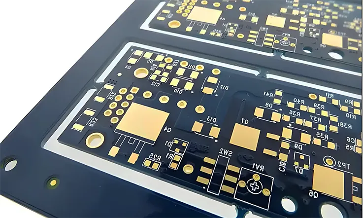
Advanced PCB Stackup Design for 4 oz Copper Multilayer Boards
When designing 4 oz copper multilayer PCBs, the stackup configuration is a main factor in ensuring both electrical performance and thermal management. For power electronic devices or industrial systems that handle high currents, the layout and arrangement of each layer must be carefully considered. An appropriate stackup maximizes current transmission efficiency while reducing signal interference and noise.
The stackup design should balance electrical performance with heat dissipation. Given the thicker 4 oz copper layers, it’s essential to manage heat flow effectively and reduce the risk of thermal stress. Additionally, the stackup structure must minimize warping or deformation caused by material stresses during the manufacturing process.
Layer Configuration for Power Distribution
The power distribution layer configuration in 4 oz copper PCBs directly influences current-carrying capability and signal integrity. By arranging power and ground layers in a well-aligned manner, PCB designers can help reduce voltage swings and suppress electromagnetic interference. Placing these planes near the signal layers allows for more stable current flow and improved overall circuit behavior.
Optimizing the layer configuration supports steady current delivery, enhances power handling, and helps minimize voltage fluctuations. This approach is widely adopted in scenarios that demand consistent electrical behavior across varying load conditions.
| Layer Type | Function | Outcome |
| Power Distribution | Distributes power to components | Minimizes voltage fluctuations |
| Ground Plane | Provides return path for current | Reduces noise and enhances stability |
| Signal Layer | Routes data and signals | Minimizes signal interference |
A well-designed power distribution layer can boost current efficiency, minimize system noise, and maintain stability across the circuit.
Via Structures and Current Flow
Via design is another factor in 4 oz copper PCBs, especially for high-current applications. Vias must be capable of handling substantial current to prevent excessive heating and maintain efficiency. Properly sized vias help ensure the current flows smoothly through the PCB without creating resistance or unwanted heat.
Power vias typically need to be larger in diameter compared to signal vias, as they are expected to handle more current. The current path should be carefully designed to minimize resistance and avoid heat buildup.
| Via Type | Characteristics | Function |
| Microvias | Smaller diameter, used for dense layouts | Best for compact designs and high-speed circuits |
| Power Vias | Larger diameter, low resistance | Carry high currents without overheating |
| Blind Vias | Connect inner layers to outer layers | Efficient in reducing complexity while allowing high current flow |
With proper via selection, high currents can be managed more efficiently, reducing the likelihood of heat-related issues in the PCB.
Copper Balance and Warpage Control
Copper balance and warpage control are some factors in multi-layer PCB design, particularly for 4 oz copper boards. During manufacturing, unequal copper distribution can cause stress, leading to warping. A balanced copper layer configuration helps prevent this issue and ensures the board remains flat and stable.
In multilayer designs, maintaining symmetry in the stackup helps reduce the chance of warping. A balanced distribution of copper thickness across layers can ease thermal stress and support mechanical stability when the board operates under high current conditions.
| Design Strategy | Purpose | Effect |
| Symmetrical Stackup | Even distribution of copper layers | Minimizes thermal and mechanical stress |
| Balanced Copper Layers | Uniform copper distribution | Prevents warping and improves stability |
Maintaining copper balance helps reduce warping issues, ensuring that the PCB performs consistently without physical distortion.
Thermal Management in 4 oz Copper PCBs: How to Improve Heat Dissipation
Effective heat control in high current circuit boards begins with how we design and select materials. For 4 oz copper PCBs, we focus on creating pathways that can draw heat away from active components without delay. This isn’t just about keeping temperatures in check — it’s about building circuits that can carry heavy loads without warping, delaminating, or creating hotspots over time. Let’s break it down and look at several proven approaches we use.
Why Thermal Conductivity Matters in Power Circuits?
In any high-current circuit, electrical losses convert into heat. If this heat isn’t redirected or dispersed, internal temperatures rise, directly affecting the functionality and stability of active and passive components.
A 4 oz Copper PCB provides a larger cross-sectional area for current flow, reducing resistive losses. But conductivity doesn’t stop at copper alone—substrate materials, board architecture, and component placement also influence how heat is handled.
Some observations from field applications:
●In LED modules, excessive junction temperature impacts light output and consistency. A board designed with thick copper, thermally conductive prepregs, and dedicated copper pours can lower junction temps by 15–30°C.
●In motor controllers, boards with no thermal pathways saw MOSFET failure under full load in under 100 hours, while revised layouts using thermal vias extended operational life by 10x.
●In energy inverters, dual-sided copper combined with ceramic substrates demonstrated superior stability even under repetitive thermal cycling.
Thermal Via Arrays and Copper Planes
Thicker copper improves lateral heat distribution, while vertical heat transfer through the board also requires attention. In such cases, thermal vias and dedicated copper planes help manage temperature flow between layers and reduce localized heat build-up.
Thermal vias are plated-through holes filled or left open, often placed under heat-generating components such as power ICs, drivers, or switching transistors. These vias transfer heat to inner or bottom layers, where copper planes then dissipate the heat over a larger area.
Effective design includes:
●High-density via grids (e.g., under QFN or D2PAK packages)
●Via stitching around hot zones, spaced within 1mm centers
●Solid internal copper layers directly connected to thermal vias
●Direct copper heatsink pads connected to exposed copper areas
By combining these tactics with a 4 oz Copper PCB layer, even the most power-dense modules can maintain steady thermal balance during operation.
FR-4 vs. Aluminum Core vs. Ceramic vs Copper Core
Choosing the right PCB substrate directly affects how well your board handles and redirects heat. While FR-4 is widely used due to cost and availability, certain high-power applications may demand alternative materials for better thermal behavior.
Here’s a comparison of popular substrate types used in heavy copper applications:
FR-4 (Standard Epoxy Glass)-
Offers stable electrical performance, but thermal conductivity is limited (~0.3–0.4 W/m·K). For moderate heat dissipation needs combined with cost-effectiveness, FR-4 with thick copper and proper via design performs reliably.
Aluminum Core (MCPCB)-
Offers a direct thermal path from component to baseplate, usually combined with dielectric layers of ~2–3 W/m·K. Common in LED modules and automotive lighting systems, where space constraints and thermal load coexist.
Ceramic (Al₂O₃ or AlN)-
Provides superior insulation and thermal transfer (up to 150–200 W/m·K in AlN). Used in EV systems, aerospace power boards, or high-reliability industrial modules.
Copper Core Substrate-
Provides unmatched conductivity and current-carrying capability. Best suited for extremely dense power converters or in environments requiring strong mechanical rigidity combined with thermal capacity. Often paired with 4 oz Copper PCB designs in dual- or multi-layer stacks.
Material Selection for 4 oz Copper PCB Manufacturing
Selecting the right combination of base materials is a decisive factor in the performance and reliability of 4 oz copper PCBs, particularly in high-current and high-temperature environments. Across heavy copper applications in LED lighting, power modules, and industrial machinery, well-considered material decisions directly influence thermal resistance, mechanical durability, and fabrication consistency. Below is a breakdown of how specific material choices contribute to building robust heavy copper boards.
High Tg FR-4 for Thermal Stability
High Tg FR-4 is frequently used as a PCB base material in the production of 4 oz copper PCBs. Its ability to withstand elevated temperatures makes it suitable for circuits exposed to repeated thermal cycles. A higher Tg rating helps maintain structural stability, reducing the likelihood of softening or delamination when heat levels fluctuate. This material is well-suited to support high-current conditions often found in power electronics. Below are some practical factors to keep in mind when selecting High Tg FR-4:
●Tg (Glass Transition Temperature) of 170°C and above ensures stable operation under thermal stress.
●Provides enhanced resistance to warping and delamination during reflow soldering and long-term operational conditions.
●Compatible with high-power devices that experience continuous temperature fluctuations.
●Suitable for designs involving large copper traces and multiple layers, ensuring long-lasting integrity.
| Property | Standard FR-4 | High Tg FR-4 |
| Tg Rating (°C) | 130-150 | 170+ |
| Thermal Stability | Moderate | High |
| Suitable for | Low-power, standard circuits | High-power, high-temp environments |
| Cost | Lower | Higher |
High Tg FR-4 provides the necessary thermal stability, making it a suitable choice for applications that demand higher durability under fluctuating heat loads.
Substrate Thickness and Conductive Layers
In heavy copper PCB design, substrate thickness directly affects both mechanical stability and thermal behavior. Thicker substrates are often selected to handle the added copper density and to enhance the board’s physical strength. For 4 oz copper PCBs, the chosen thickness aims to strike a balance between load-bearing capacity and effective heat distribution, all while maintaining reliable electrical characteristics.
●Typical substrate thicknesses range from 1.6 mm to 3.2 mm, depending on the size of the board and current load.
●Multi-layer stackups (typically 4-6 layers) are often employed to better distribute power and heat.
●Increased substrate thickness improves mechanical strength and reduces board warping during manufacturing and operation.
●Thicker substrates support larger copper pours and are better suited for applications that require heat dissipation and electrical isolation.
| Substrate Thickness | Suitable for Applications | Benefits |
| 1.6 mm | Low to medium current circuits | Cost-effective, versatile |
| 2.4 mm | Power devices, moderate heat dissipation needs | Enhanced mechanical support |
| 3.2 mm | High-power devices, large copper traces | Improved heat dissipation, stability |
By carefully selecting substrate thicknesses, PCB manufacturers can ensure the board can handle the increased current demands and provide the needed thermal management.
Copper Foil Types and Specifications
The choice of copper foil type has a direct impact on the electrical performance, heat distribution, and long-term reliability of 4 oz copper PCBs. Different types of copper foil, such as electrodeposited (ED) and rolled-annealed (RA), each have specific properties that make them suitable for particular applications.
●ED Copper: Most commonly used, provides good adhesion and is cost-effective for standard PCB designs.
●RA Copper: Offers superior ductility and is reliable for designs requiring flexibility or resistance to mechanical stress.
●Reverse-Treated Copper: Ensures better adhesion and is often used in applications that undergo repeated thermal cycling.
●Low-Profile Copper: Reduces surface roughness, improving signal integrity in high-frequency designs.
| Copper Type | Characteristics | Common Use Cases |
| ED Copper | Good adhesion, affordable | Standard PCBs, power circuits |
| RA Copper | High ductility, more flexible | Automotive, flexible designs |
| Reverse-Treated | Better adhesion under thermal stress | High-temperature applications |
| Low-Profile Copper | Reduced surface roughness | High-frequency circuits |
The selection of copper foil type must be aligned with both the physical requirements of the board and the specific needs of the application, such as flexibility, mechanical strength, or signal integrity.
Common Manufacturing Challenges with 4 oz Copper PCBs and How to Overcome Them?
When working with 4 oz copper PCBs, we often face unique challenges. These boards, which are designed to handle high currents and power dissipation, demand precision during manufacturing to ensure functionality and longevity. Below, we explore some of the most common hurdles encountered when producing 4 oz copper PCBs and provide actionable solutions to address them.
Etch-Back Control for Thick Copper
Etching copper to create the circuit traces on thick copper PCBs, such as those using 4 oz copper, is more challenging compared to standard copper boards. The thicker copper requires more precise etch-back control to avoid over-etching, which can result in uneven trace width or poor electrical performance.
When handling thicker copper, the etching process needs to be finely tuned to remove just the right amount of material. If the copper layer is etched back too much, the traces may become too thin to handle the intended current load. Conversely, under-etching can lead to inadequate trace width, which can cause higher resistance and thermal issues.
Here’s how to ensure proper etch-back control:
Step 1: Use an etching solution designed for thicker copper, with controlled temperature and agitation.
Step 2: Adjust exposure times in the etching process to allow for the precise removal of copper.
Step 3: Inspect the etched areas frequently to ensure trace uniformity and thickness.
| Copper Thickness | Recommended Etch Time | Solution Type |
| 4 oz | 30-45 minutes | Alkaline solution |
| 2 oz | 20-30 minutes | Acidic solution |
With proper control over the etch-back process, we can ensure that traces are both strong and capable of handling high currents without compromise.
Managing Delamination Under Load
Delamination, or the separation of layers within the PCB, is a common problem in thicker copper PCBs. The more copper used in the PCB, the greater the risk of internal stresses, especially during thermal cycling or under mechanical load. In 4 oz copper PCBs, the added thickness increases the internal strain, potentially leading to delamination if not managed properly.
To prevent delamination:
●Use of High-Tg Materials: High-Tg (glass transition temperature) materials for the substrate can better withstand temperature changes without the risk of layer separation. These materials help the PCB endure higher thermal stresses, especially in heavy-duty applications like power supplies or industrial systems.
●Controlled Curing Process: During lamination, it’s essential to control the pressure and temperature to ensure proper bonding between layers. This prevents the board from undergoing unnecessary mechanical stress that could lead to delamination.
For example, PCBs used in high-current applications like power distribution require robust bonding layers. Without effective management of thermal expansion and mechanical forces, the board can fail under prolonged use, resulting in poor performance or complete system failure.
| Substrate Type | Tg Value (°C) | Recommended Applications |
| Standard FR-4 | 130-150°C | General-purpose, low power |
| High-Tg FR-4 | 170-180°C | Power circuits, industrial |
| Ceramic Core | 250°C | Extreme heat applications |
By selecting materials with higher thermal properties and refining the curing process, delamination risks can be minimized, extending the lifespan of the 4 oz copper PCB.
Via Hole Plating with Heavy Copper
Plating via holes in 4 oz copper PCBs comes with added complexity. Unlike standard boards where via holes require only a thin copper layer, these high-copper-weight designs demand much thicker and more consistent plating. The process must support uniform copper buildup, particularly around the via walls, to maintain electrical continuity and support high current flow without creating weak points or resistance jumps.
Improper via plating can lead to several issues, such as:
●Inconsistent Current Flow: Uneven plating may cause increased resistance, which can result in voltage drops and inefficiency.
●Weak Vias: If the via holes are not plated sufficiently, they may fail to carry the required current, leading to PCB failure.
To improve via hole plating with heavy copper:
Step 1: Use a multi-step plating process to gradually build up the copper layer inside the vias, ensuring uniform deposition.
Step 2: Implement pulse plating techniques to ensure a more consistent copper layer, especially in deep vias or thick copper PCBs.
Step 3: Conduct regular inspections using X-ray or ultrasonic testing to check for plating defects in vias.
| Plating Process Type | Advantages | Application |
| Pulse Plating | Provides better control of copper thickness | Heavy copper PCBs with deep vias |
| Conventional Plating | Faster process, suitable for thinner layers | Standard copper PCBs |
| Electroplating | Uniform coating on via walls and barrels | High-current PCBs |
How to Choose the Right Heavy Copper PCB Manufacturer?
Selecting a manufacturer for your heavy copper PCB should be based on their ability to meet the performance and reliability demands of high-current designs. These boards are frequently used in power-intensive circuits, where consistent production processes, advanced equipment, and proven track records matter. In this section, we’ll explore the factors that help you evaluate and compare manufacturing partners for your 4 oz copper PCB projects — without the fluff, just the real nuts and bolts.
Experience in High-Current Product Lines
When selecting a manufacturer, the first thing to consider is their experience with high-current applications. Heavy copper PCBs are often used in circuits that require high current handling, such as power distribution systems, automotive electronics, or industrial equipment. A manufacturer with experience in these areas will be familiar with the technical challenges and design considerations unique to high-current circuits.
What to Look For:
●Proven Project Portfolio: Look for manufacturers that have experience working on similar products. This could include power converters, chargers, or motor controllers. A company with a history of delivering successful high-current designs is more likely to understand the intricacies of heavy copper manufacturing.
●Expertise in Current Density Management: A reliable manufacturer should have a thorough understanding of managing high current densities. They should offer advanced solutions like thicker copper layers and carefully optimized trace widths to handle the load.
Technical Support for OEM Integration
Technical support is also an aspect worth considering when selecting a PCB manufacturer. For original equipment manufacturers (OEMs), the process continues beyond the delivery of the bare boards. Effective integration into the end system often requires coordination, design validation, and prompt response to technical inquiries. Selecting a partner that provides consistent support throughout each project stage—from initial layout to final implementation—can contribute to a more streamlined development process.
Support to Expect:
●Design Collaboration: Ensure the manufacturer offers collaborative support to help refine the design for production. This includes addressing challenges like trace routing, thermal management, and ensuring proper alignment of vias and copper pours.
●Prototype to Production Assistance: Working with a manufacturer that can support both the prototype phase and large-scale production is must. They should assist in developing test cases, ensuring design accuracy, and identifying any potential flaws early in the process.
Certifications, NDA, and Confidentiality
It’s essential that the manufacturer complies with industry standards and has processes in place to protect intellectual property. Certifications not only demonstrate that the manufacturer follows recognized best practices but also indicate a commitment to quality and safety. Additionally, confidentiality is a major concern when dealing with sensitive designs.
Things to Check:
●Industry Certifications: Look for certifications like ISO 9001 (quality management), UL (safety), and IPC-2221 (PCB design standards). These ensure the manufacturer operates at a high standard of production and safety.
●Non-Disclosure Agreements (NDAs): For OEMs, maintaining confidentiality around proprietary layouts and technical documents requires clear agreements. It’s advisable to work with a supplier that readily accepts non-disclosure terms to help prevent unauthorized sharing or use of sensitive design data.
●Regulatory Compliance: Manufacturers should comply with international standards such as RoHS (Restriction of Hazardous Substances) and REACH (Registration, Evaluation, Authorisation, and Restriction of Chemicals) if relevant to your product. This ensures that the materials used are safe and meet environmental standards.
Why JarnisTech is a Trusted Heavy Copper PCB Manufacturer?
When it comes to heavy copper PCBs, finding the right manufacturer is all about reliability, precision, and the ability to meet strict specifications. JarnisTech has built a strong reputation for providing consistent, high-performance PCBs that cater to industries requiring specialized solutions for high-current and high-power applications. This section outlines why us is a preferred partner across various global markets.
Manufacturing Capabilities and Equipment
JarnisTech utilizes cutting-edge machinery and advanced manufacturing techniques to produce heavy copper PCBs that meet stringent performance requirements. With the ability to handle high-current product lines, JarnisTech’s equipment ensures precise etching, plating, and layer stacking, delivering products that can manage increased electrical loads without compromising reliability.
Here’s a look at their manufacturing process:
| Process | Technology Used | Benefits |
| Copper Etching | Laser Direct Imaging (LDI) | High precision for fine traces and consistent results |
| Via Drilling | Laser Drilling | High-speed, precise hole drilling for heavy copper |
| Plating | Electrolytic Copper Plating | Even copper deposition for thick copper applications |
| Testing | Automated Optical Inspection (AOI) | Ensures no defects in copper traces or layer integrity |
This machinery allows for smooth handling of both thick copper layers and complex designs, which are often required in high-power electronic applications.
Client Industries and Case Studies
JarnisTech supports a wide range of industries, including telecommunications, automotive, renewable energy, and industrial electronics. our ability to produce custom heavy copper PCBs for each of these sectors has positioned us as a reliable provider for high-current PCB needs.
Here’s a breakdown of key industries served and the application areas:
| Industry | Applications | PCB Features |
| Telecommunications | Base stations, RF circuits, power amplifiers | High thermal conductivity, large current handling |
| Automotive | Electric vehicles, power systems, control units | High-power efficiency, shock resistance |
| Renewable Energy | Inverters, solar panels, wind turbines | Enhanced heat dissipation, energy efficiency |
| Industrial Electronics | Industrial controllers, robotics | Durability, power management |
These industries demand heavy copper PCBs due to their need for efficient heat dissipation and the ability to handle high electrical currents. JarnisTech has successfully met these needs through its focused product development and manufacturing expertise.
International Delivery and Support
JarnisTech is equipped with a global supply chain network, ensuring that their heavy copper PCBs are delivered worldwide. From North America to Europe, Asia, and beyond, JarnisTech has streamlined logistics to ensure timely delivery without compromising quality.
Here’s a breakdown of JarnisTech’s delivery capabilities:
| Region | Average Delivery Time | Logistics Support |
| North America | 3-5 business days | Domestic courier partnerships |
| Europe | 5-7 business days | Customs clearance management |
| Asia | 4-6 business days | Expedited international shipping |
| Rest of the World | 7-10 business days | Integrated global distribution |
In addition to reliable delivery, we offers comprehensive technical support, assisting clients at every stage from pre-production to after-sales. Clients who require help with design optimization or need guidance on complex integration can rely on JarnisTech’s consistent involvement to support successful outcomes throughout the process.
FAQs About 4 oz Copper PCB
1.Can 4 oz copper PCBs be used for RF (radio frequency) applications?
4 oz copper is not typically suited for RF applications because its increased copper thickness may lead to signal integrity issues due to higher resistance and parasitic inductance.
2.Do 4 oz copper PCBs have better thermal cycling resistance than standard PCBs?
Yes, thicker copper can improve thermal cycling resistance by reducing the amount of thermal expansion and contraction during temperature fluctuations.
3.What is the maximum operating temperature for 4 oz copper PCBs?
The maximum operating temperature generally ranges from 100°C to 130°C, depending on the substrate material used, but can be higher with specific design optimizations.
4.How does copper thickness affect PCB bending and flexibility?
Thicker copper can reduce the flexibility of the PCB, making it more rigid, which can be a challenge in applications requiring flexibility.
5.Can 4 oz copper PCBs be used in high-voltage applications?
Yes, they are suitable for high-voltage applications, provided the design includes proper insulation and spacing to avoid short circuits or arcing.
6.What is the difference between 4 oz copper and 6 oz copper PCBs?
6 oz copper offers even higher current-carrying capacity and improved heat dissipation compared to 4 oz copper, but requires more advanced manufacturing techniques.


