
In the modern electronics, managing high currents presents a persistent engineering challenge. A robust and practical approach to this issue is the utilization of 6 oz copper printed circuit boards (PCBs). This specific copper thickness is engineered to substantially increase the current-carrying capacity of PCB applications, facilitating efficient and reliable operation in high-power circuits. This guide provides a clear and detailed understanding of the design, production, and material properties required for 6 oz copper PCB circuit boards, offering technical details for advanced applications.
Executive Summary:
For professionals requiring a rapid understanding of the core concepts, here are the takeaways from this guide:
1.Definition & Value: 6 oz copper PCBs feature a copper layer thickness of approximately 210µm, six times that of standard 1 oz PCBs. This enables them to carry high currents of several tens of amperes while significantly reducing circuit resistance and power loss.
2.Core Performance Advantages: Beyond superior current handling, 6 oz copper provides excellent thermal management (dissipating heat through the copper itself) and enhanced mechanical strength and durability, especially against vibration and thermal cycling.
3.Design & Manufacturing Complexity: Successful implementation requires precise engineering, including thermal management simulation, specialized lamination strategies, and overcoming technical challenges in etching, drilling, and assembly.
4.Cutting-Edge Technologies: To achieve extreme power density, advanced techniques like planar magnetics, embedded copper coins, and buried bus bars can be used to integrate components and high-current pathways directly into the PCB structure, demanding elite manufacturing capabilities.
5.Application Areas: 6 oz copper PCBs are an indispensable foundation for high-power sectors, including electric vehicle (EV) powertrains, renewable energy inverters, industrial power supplies, and telecommunications infrastructure.
Foundational Concepts of Heavy Copper PCBs
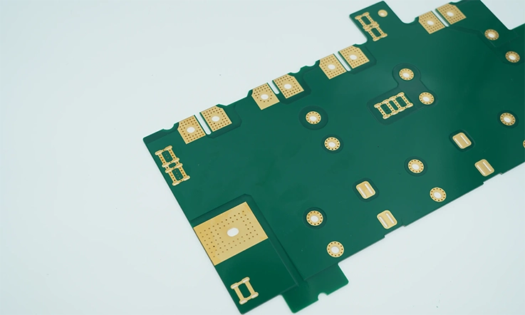
Understanding the principles behind heavy copper PCBs is the first step toward leveraging their capabilities. The term “heavy copper” refers to PCBs with copper layers thicker than the standard 1 or 2 ounces per square foot. A 6 oz copper board represents a significant step up in thermal and electrical performance.
Defining Copper Weight in PCB Fabrication
●PCB copper weight is a measure of the thickness of copper foil on a given surface area. It is expressed in ounces per square foot (oz/ft2).
●A 1 oz copper designation means that one ounce of copper is spread evenly over a one-square-foot area. This corresponds to a thickness of approximately 35 micrometers (μm) or 1.37 mils.
●Consequently, a 6 oz copper PCB has a copper layer with a thickness of about 210 μm (8.2 mils), six times thicker than the standard 1 oz board. This substantial increase in copper mass is directly responsible for its enhanced properties.
Distinguishing 6 oz Copper from Standard PCBs (1-2 oz)
●Standard PCBs, typically using 1 oz or 2 oz copper, are sufficient for low-power digital and analog signal processing. They become a performance bottleneck when circuit designs move into high-power domains.
●6 oz copper PCBs are specifically constructed to manage the heat and demanding electrical loads of power-hungry circuits. The thicker copper offers a distinct performance margin in sectors where heat buildup and power surges are common, making it a good choice for applications that demand stable and reliable operation.
The Relationship Between Copper Thickness and Current-Carrying Capacity
●The current-carrying capacity of a PCB trace is fundamentally limited by its cross-sectional area and the allowable temperature rise.
●A thicker copper layer, as found in a 6 oz PCB, provides a much larger cross-sectional area for a given trace width.
●According to Ohm’s law and principles of electrical resistance, a larger cross-sectional area results in lower DC resistance (R=ρAL, where A is the area). This reduction in resistance minimizes power loss (as heat, P=I2R) and allows the trace to conduct higher currents for the same temperature increase.
Core Performance Advantages of 6 oz Copper Foil
The adoption of 6 oz copper in PCB design is driven by a set of tangible performance benefits that directly address the limitations of standard boards in demanding applications. These advantages extend beyond simple current handling to include thermal performance and mechanical robustness.
Superior Current Handling Capabilities
The primary benefit of 6 oz copper is its capacity to handle substantial currents without risking overheating or circuit degradation. The increased conductor thickness allows for the design of compact, high-power-density boards, which is beneficial for power electronics and EV charging stations.
Enhanced Thermal Dissipation and Management
Heat is a primary byproduct of high-current circuits. The increased volume of copper in a 6 oz PCB acts as an effective heat spreader, distributing thermal energy more efficiently across the board. This improved thermal management keeps components operating at lower temperatures, enhancing the overall longevity and reliability of the assembly.
Increased Mechanical Strength and Durability
The thicker copper layers add significant rigidity and strength to the PCB structure. This makes the board more resilient to mechanical stress, such as vibration and physical shock. The plated through-holes (PTHs) in a 6 oz board are also more robust, reducing the risk of barrel cracking or pad lifting during thermal cycling or assembly. This is a considerable advantage in harsh industrial and automotive environments.
Reduced Signal Loss and Lowered Trace Resistance
For high-performance applications, maintaining signal integrity is a central consideration. The lower trace resistance inherent in 6 oz copper helps minimize voltage drop (Vdrop=I×R) over long traces and reduces signal degradation. This results in a cleaner, more efficient power delivery to components and can be beneficial in certain high-speed applications where power and signal planes are in close proximity.
Advanced Design and Engineering for 6 oz Copper PCBs
Designing a 6 oz copper PCB is a task that requires a precise understanding of electrical and thermal principles. These boards must be engineered not just to conduct high currents but also to manage the resulting heat while maintaining signal integrity and long-term reliability.
Trace Width and Spacing Calculations for High-Current Loads
●Proper trace width calculation is a foundational aspect of heavy copper design. The copper traces must be sized appropriately to handle the intended current without excessive temperature rise.
●Industry standards like IPC-2221 provide baseline formulas for calculating trace width based on current, copper thickness, and allowable temperature rise. For a 6 oz PCB, these calculations will yield narrower traces for a given current compared to a 1 oz board, enabling higher density designs.
●Spacing between high-current traces is also a consideration to prevent electrical arcing and manage thermal crosstalk between adjacent conductors.
Layer Stack-up Strategies in Multilayer Heavy Copper Boards
●In multilayer 6 oz copper PCBs, the layer stack-up is engineered to optimize both electrical performance and thermal dissipation.
●Placing high-current layers internally can help contain EMI, while using external layers allows for better heat dissipation into the ambient environment, often with the aid of heat sinks.
●The choice and thickness of dielectric materials (prepreg and core) between the heavy copper layers are adjusted to meet impedance requirements and ensure proper bonding and insulation. This expertise in multilayer stack-up design is a hallmark of advanced fabrication capabilities.
Impedance Control Nuances with Thick Copper Traces
●While often used in power applications, heavy copper can be present in mixed-signal boards requiring impedance control. The thickness of 6 oz copper significantly alters the trace geometry and, therefore, its characteristic impedance.
●The trapezoidal shape of etched thick copper traces (due to the etching process) must be accounted for in impedance modeling. Advanced simulation software is used to accurately predict impedance, adjusting trace width and dielectric spacing to hit targets like 50 Ω or 100 Ω differential pairs.
Component Placement and Layout for Thermal Optimization
●The physical placement of components on a 6 oz copper PCB directly influences its thermal performance.
●High-power components like MOSFETs, rectifiers, and power resistors should be distributed across the board to avoid creating localized hotspots.
●Placing these components near the board’s edge or adjacent to thermal vias and copper planes facilitates the transfer of heat away from the device and into larger thermal masses or attached heat sinks.
Specialized Fabrication Processes for 6 oz Copper PCBs
Fabricating 6 oz copper PCBs demands specialized equipment and precise process control beyond what is required for standard boards. The thickness of the copper presents unique challenges at nearly every stage of production.
Material Selection: Substrates and High-Purity Copper Foils
●The process begins with selecting the right materials. High-purity copper foil with a nominal thickness of 6 oz per square foot is the starting point.
●The base substrate material, such as high-temperature FR-4 (FR4-HTG), polyimide, or specialized metal-core materials, must be chosen for its thermal stability and ability to withstand the higher temperatures and longer press cycles used in heavy copper lamination. UL-certified materials are often specified to guarantee compliance with safety and performance standards.
Precision Etching and Plating Techniques
●Etching 210 μm of copper requires different techniques than etching 35 μm. A longer exposure to chemical etchants is needed, which increases the risk of “undercutting”—where the etchant removes copper laterally beneath the photoresist.
●To counteract this, specialized etching solutions and advanced photolithography processes are employed to achieve straight, well-defined trace sidewalls.
●Plating processes, especially for filling vias and building up trace thickness, must be carefully controlled to ensure uniform copper deposition across the entire board surface, including inside small-diameter holes.
Lamination and Bonding Challenges in Multilayer Builds
●Laminating multilayer boards with 6 oz copper layers is complex. The significant thickness of the copper traces creates a topology with large “hills and valleys.”
●Sufficient resin flow from the prepreg material is needed to completely fill these gaps and prevent air voids, which could lead to delamination or electrical failures. This often requires multiple sheets of prepreg and carefully controlled lamination press cycles (temperature, pressure, and time).
Drilling, Routing, and Finishing Operations
●Drilling through 6 oz copper is more demanding on drill bits, causing increased wear and heat. Slower drill speeds and specialized drill geometries are used to prevent burrs and ensure clean, smooth holes.
●Similarly, routing (cutting) the final board profile from the panel requires high-torque spindles and robust router bits to cut cleanly through the thick copper without delaminating the board edges.
●Finally, surface finishes like ENIG (Electroless Nickel Immersion Gold) or Lead-Free HASL (Hot Air Solder Leveling) must be applied with processes adjusted for the heavy copper features to ensure a flat, solderable surface.
Planar and Embedded Technologies for Extreme Power Density
As power conversion systems demand ever-increasing efficiency and smaller form factors, conventional PCB traces—even heavy copper ones—can reach their limits. To push beyond these boundaries, advanced fabrication techniques are used to integrate components directly into the PCB structure itself. These planar and embedded technologies represent the pinnacle of power density and thermal management, requiring a deep synergy between electrical design and state-of-the-art manufacturing.
Planar Magnetics: Integrating Inductors and Transformers into the PCB Stack-up
●Concept: Planar magnetics replace traditional wire-wound inductors and transformers with windings created from copper traces within a multilayer PCB. These traces, often in spiral or concentric patterns across multiple layers, are then coupled through a low-profile ferrite core that is physically inserted into or around the PCB.
●Design and Production: The design involves complex electromagnetic modeling to achieve the desired inductance and current handling. Heavy copper traces, such as 6 oz, are often used for the windings to minimize resistive losses (I2R). From a production standpoint, this requires exceptional layer-to-layer registration accuracy to align the winding segments perfectly. Furthermore, high-current vias are needed to connect the windings between layers, and the lamination process must be precisely controlled to accommodate the ferrite core cutout without creating stress or voids.
●Performance Benefits: This approach yields significant advantages. The resulting magnetic components have an extremely low profile, ideal for height-constrained applications. Thermal performance is superior, as heat generated in the copper windings is conducted directly into the PCB’s copper planes and dissipated over a large area. This integration also reduces electromagnetic interference (EMI) and offers high repeatability from board to board.
Embedded Copper Coins and Slugs for Targeted Thermal Management
●Concept: This technology involves embedding a solid, pre-machined copper block (a “coin” or “slug”) into a cavity within the PCB during the lamination cycle. The top surface of the coin can be made flush with the PCB surface, allowing a high-power component like a GaN FET, power MOSFET, or high-output LED to be mounted directly onto it.
●Design and Production: The design process involves co-designing the PCB layout and the coin’s geometry. The coin provides a landing pad for the component and may have features like pedestals or through-holes. The production process is highly advanced: it involves CNC machining the PCB to create a precise cavity, press-fitting the coin, and then using a carefully managed lamination cycle with specialized prepregs to bond the entire structure seamlessly.
●Performance Benefits: The primary advantage is the creation of an ultra-low thermal resistance path. Heat flows directly from the component through the solid copper coin to a heat sink on the other side of the board, effectively bypassing the thermally resistive PCB dielectric materials (like FR-4). This is one of the most effective methods for managing intense, localized hotspots.
Buried Bus Bars for High-Current Power Distribution
●Concept: For applications requiring current distribution far beyond what even wide 6 oz traces can handle, thick, pre-fabricated copper or aluminum bars can be embedded within the PCB’s internal layers. These are known as buried or embedded bus bars.
●Design and Production: The design requires careful planning of the bus bar’s path to avoid interference with other components and routes. A robust connection strategy, typically using multiple rows of large-diameter vias, must be designed to link the buried bar to the surface layers. The production is a multi-step lamination process. A sub-assembly is created, the bus bar is placed in a routed channel, and then the final layers are laminated on top. Managing the coefficient of thermal expansion (CTE) mismatch between the massive metal bar and the surrounding laminate is a significant challenge that requires advanced material science and press-cycle control.
●Performance Benefits: This technique enables the distribution of hundreds of amps within the profile of the PCB, saving space and eliminating the need for bulky external wiring. It provides a structurally sound, low-inductance power path that is shielded from EMI by the outer layers of the board.
Thermal Management Solutions for High-Heat Environments
Effective thermal management is non-negotiable for the successful implementation of 6 oz copper PCBs in high-power systems. The design must not only accommodate high currents but also provide a clear path for the resulting heat to dissipate.
The Function of Thermal Vias and Heat Sinks
●Thermal vias are a primary tool for thermal management. These are essentially plated through-holes placed under or around heat-generating components. They create a low-thermal-resistance path to conduct heat from the top layer of the PCB to internal or bottom copper planes.
●These copper planes then act as large heat spreaders. For even greater heat dissipation, an external heat sink can be mechanically attached to these planes, allowing heat to transfer to the surrounding air via convection.
Comparing Active vs. Passive Cooling Strategies
●Passive Cooling relies on natural convection and radiation to dissipate heat. It includes features like heat sinks, thermal vias, and large copper planes. It is simple, reliable, and cost-effective, suitable for many applications.
●Active Cooling involves the use of fans or liquid cooling systems to forcibly remove heat. This approach is used when passive methods are insufficient to keep component temperatures within safe operating limits, such as in densely packed power supplies or high-power computing systems. A 6 oz copper PCB is often the foundation upon which these active cooling solutions are built.
| Cooling Type | Advantages | Disadvantages | Optimal Use Case |
| Passive Cooling | Simple, no power required, silent, cost-effective | Lower efficiency, may require large surface area | Consumer electronics, mid-range power systems |
| Active Cooling | High efficiency, adaptable to extreme power levels | Adds complexity, cost, noise, and requires power | High-power industrial systems, data centers |
Design Techniques to Minimize Heat Accumulation
●Beyond vias and heat sinks, layout design itself can significantly impact heat management.
●Using wider traces for high-current paths not only handles the current but also helps spread heat over a larger area, reducing the peak temperature.
●Strategic layer stacking can isolate sensitive components from high-heat layers, and internal copper planes can be designed to draw heat away from populated areas of the board.
Thermal Simulation and Modeling for Predictive Analysis
●Before fabrication, advanced thermal simulation software (e.g., Ansys Icepak) is used to model the thermal behavior of the PCB design under load.
●These simulations predict heat distribution, identify potential hotspots, and allow for optimization of the layout, component placement, and cooling solutions. This predictive analysis reduces the need for multiple physical prototypes and shortens the design cycle.
Signal Integrity Considerations in Heavy Copper Designs
While primarily associated with power electronics, 6 oz copper PCBs are sometimes used in mixed-signal environments where maintaining signal integrity is a serious consideration. The unique physical properties of thick copper traces introduce specific challenges that must be addressed during the design phase.
Mitigating Crosstalk and EMI with Ground Planes
●High-current switching in power circuits can generate significant electromagnetic interference (EMI). A well-designed ground plane is the first line of defense.
●In a 6 oz copper multilayer PCB, solid ground planes provide a low-impedance return path for currents, which helps contain electromagnetic fields and reduce noise coupling (crosstalk) to adjacent signal traces. The thickness of the copper enhances the effectiveness of the ground plane.
Impact of Thick Copper on High-Frequency Signal Propagation
●For high-frequency signals, the “skin effect” becomes pronounced. This phenomenon causes current to flow predominantly on the outer surface (or “skin”) of a conductor.
●The rough surface profile of thick copper foil can increase the path length for these high-frequency currents, leading to higher-than-expected signal attenuation. The geometry of the trace, including the trapezoidal cross-section from etching, also affects signal propagation and must be accurately modeled.
Return Path Management in High-Power Circuits
●In any circuit, the current must have a continuous return path to its source. In high-current applications, a poorly managed return path can create large current loops, which act as antennas, radiating EMI.
●Designers must ensure that a clear, low-inductance return path exists directly beneath high-current traces, typically through a dedicated ground plane. Any splits or gaps in this return path can force the current to detour, increasing inductance and degrading both power and signal integrity.
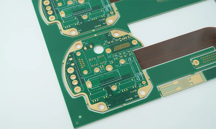
Application of 6 oz Copper in Multilayer and Rigid-Flex PCBs
The capabilities of 6 oz copper are not limited to simple, single-layer boards. Advanced fabrication allows for its integration into complex multilayer and rigid-flex PCBs, enabling innovative solutions for challenging electromechanical applications, particularly in the automotive and aerospace sectors. This demonstrates a high level of manufacturing prowess.
Engineering Rigid-Flex PCBs for High-Current Automotive Systems
●Rigid-flex PCBs combine rigid sections for component mounting with flexible sections that allow the board to be bent or folded. This is useful for fitting electronics into tight, irregularly shaped spaces, like in modern vehicles.
●Incorporating 6 oz copper into a rigid-flex design allows high-power circuits to be routed through the assembly without separate, bulky wiring harnesses. This requires specialized materials and processes to ensure the flexible sections can withstand the mechanical stress of bending while carrying high currents.
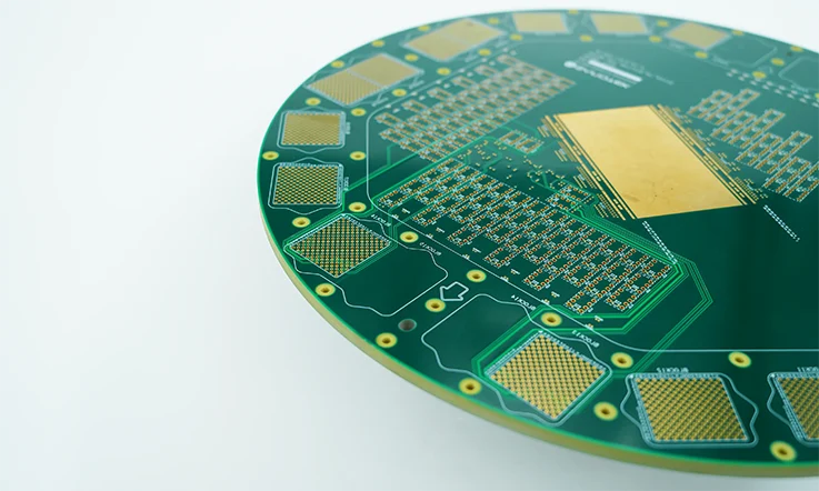
Building Complex Multilayer Boards for Power Distribution
●Modern power distribution systems, such as those in data center servers or telecommunications equipment, often require complex multilayer PCBs with multiple power and ground planes.
●Using 6 oz copper for these planes provides very low resistance and excellent thermal spreading. Fabricating a 10+ layer board where some or all layers are 6 oz copper is a significant manufacturing feat, requiring expertise in lamination, drilling, and plating to ensure layer-to-layer registration and connectivity.
Overcoming Fabrication Complexities of Combined Technologies
●The combination of heavy copper with flexible substrates or many layers introduces unique fabrication hurdles.
●Differential etching is sometimes required, where different copper weights on the same layer are etched in multiple steps. Adhesion of the thick copper to flexible polyimide substrates must be carefully managed. The entire process requires a deep integration of chemical, mechanical, and electrical engineering principles.
Comparative Analysis: 6 oz Copper vs. Alternative High-Current Solutions
While 6 oz copper PCBs offer a powerful, integrated solution for many high-current applications, they are not the only option. Understanding the alternatives is beneficial for making an reliable engineering decision based on specific project requirements for current, space, cost, and thermal performance.
Solution 1: Extremely Heavy Copper PCBs (8 oz and above)
●Description: This approach simply increases the copper weight further, to 8 oz, 10 oz, or even 20 oz. This provides even greater current capacity and thermal dissipation through the PCB itself.
●Advantages: It keeps the solution fully integrated within the PCB, eliminating the need for external components. It offers the highest possible current capacity within a standard PCB form factor.
●Disadvantages: Fabrication becomes exponentially more difficult and expensive. Etching fine features is nearly impossible, lamination yields can decrease, and drilling creates extreme tool wear. The board becomes extremely rigid and heavy. This is a niche solution for extreme power density requirements.
Solution 2: Laminated Bus Bars
●Description: Bus bars are prefabricated, laminated structures of conductive material (typically copper or aluminum) insulated from each other. They are mechanically mounted to the PCB to distribute high currents.
●Advantages: They can handle extremely high currents (hundreds or thousands of amps), far beyond what any PCB can manage alone. They have very low resistance and inductance, offering excellent electrical performance for power distribution.
●Disadvantages: They are a separate component that adds assembly steps, cost, and weight. They are not integrated into the PCB layers, which can create design challenges in compact systems. They offer less flexibility in routing compared to PCB traces.
Solution 3: Embedded Copper Coin Technology
●Description: This advanced technique involves embedding a solid piece of copper—a “coin”—into a cutout within the PCB during the lamination process. The top of the coin is flush with the PCB surface for direct component mounting.
●Advantages: It provides an unparalleled direct thermal path from a component (like a high-power FET) to an external heat sink, bypassing the PCB’s dielectric material. This offers superior local thermal management. The coin itself can also be shaped to carry very high currents.
●Disadvantages: This is a complex and expensive manufacturing process. It requires precise machining of the coin and the PCB cutout, as well as specialized lamination processes. It is typically used for localized “hotspot” management rather than board-wide current distribution.
| Feature | 6 oz Copper PCB | Bus Bar | Embedded Copper Coin |
| Current Capacity | High (tens of amps) | Very High (hundreds+ of amps) | High to Very High (localized) |
| Integration | Fully integrated in PCB | Separate component, requires assembly | Fully integrated in PCB |
| Thermal Path | Good (through copper planes) | N/A (separate) | Excellent (direct metal path) |
| Design Flexibility | High | Low | Medium (localized) |
| Cost | Medium-High | High | Very High |
| Best For | Integrated power electronics, automotive, industrial controls. | Centralized power distribution, switchgear, large inverters. | Extreme hotspot cooling for single high-power components. |
Dominant Industry Applications
As industries push toward more powerful and energy-efficient electronics, the need for robust PCB solutions like 6 oz copper is accelerating. Several core sectors rely on these boards to meet the demanding requirements of their high-power systems.
Automotive Sector: EV Powertrains and Battery Management Systems
The shift to electric mobility is a major driver for heavy copper PCBs. Electric vehicle (EV) manufacturers need dependable power distribution for battery management systems (BMS), inverters, and onboard chargers. 6 oz copper PCBs help maintain stability in these high-current systems, especially during fast-charging cycles where power demands are extreme.
Renewable Energy: Solar Inverters and Wind Turbine Controllers
Solar power inverters and wind turbine controllers must efficiently handle large amounts of current while operating in harsh outdoor environments. 6 oz copper PCBs provide the necessary current capacity and thermal efficiency, ensuring these systems are durable and perform optimally under high-stress conditions.
Industrial Automation and Power Supply Units
From factory floor motor controls to uninterruptible power supplies (UPS), industrial electronics depend on robust power handling. 6 oz copper PCBs are used to manage high-current systems in these demanding environments, where reliability under extreme temperatures and mechanical stress is a prerequisite.
Telecommunications Infrastructure
Telecommunications networks, including 5G base stations and data center equipment, require reliable power systems that handle substantial currents without compromising signal integrity. 6 oz copper PCBs facilitate efficient power distribution while minimizing the risk of overheating and signal loss in these high-availability systems.
Application Case Study: Designing a 6 oz Copper PCB for an EV On-Board Charger
To make the preceding technical concepts more tangible, this case study examines the application of a 6 oz copper PCB in a high-power Electric Vehicle On-Board Charger (OBC).
Project Requirements
●Power Level: 7.2kW, supporting a single-phase AC input (~240V @ 30A).
●Output: Charging a 400V battery system with an output current of approximately 18A.
●Physical Constraints: Strict dimensional limits to fit within the vehicle’s confined installation space.
●Cooling Method: Liquid-cooled via a cold plate, requiring the PCB to efficiently conduct heat to the cooling plate.
Design and Material Selection
●Justification for 6 oz Copper: The design team determined that a multilayer 6 oz copper board offered higher integration and fewer assembly steps compared to a “2 oz copper + external bus bar” approach, while also leveraging the PCB itself as a medium for heat conduction and spreading.
●Material: A high-glass-transition-temperature (High-Tg) FR-4 material was selected to ensure the PCB substrate maintains its mechanical stability and electrical properties in the high-temperature operating environment of the OBC.
Thermal and Electrical Co-Design
●Routing and Thermal Path: The required minimum trace widths for the >30A AC input path and the ~20A DC output path were calculated according to IPC-2221 standards. In the main power stages, such as the Power Factor Correction (PFC) and LLC resonant converter, the areas beneath the switching devices (MOSFETs/IGBTs) were densely populated with thermal vias to conduct heat directly to the bottom layer, which interfaces with the liquid-cooled plate.
●Localized Heat Mitigation: For the area of highest heat concentration, the rectifier bridge, an embedded copper coin was designed into the PCB. The coin was directly embedded, with its top surface serving as the mounting pad for the rectifier and its bottom surface making direct contact with the cold plate, creating a “thermal superhighway” of extremely low thermal resistance.
Fabrication and Assembly Strategy
●Fabrication: To manage the significant topographical variations caused by the 6 oz copper layers, a multi-stage resin fill and lamination process was employed to ensure a void-free structure, enhancing long-term reliability. ENEPIG (Electroless Nickel Electroless Palladium Immersion Gold) was chosen as the surface finish to meet the stringent reliability and anti-vibration requirements of automotive-grade applications.
●Assembly: A custom reflow soldering profile was developed, featuring an extended preheat and soak stage. This ensured the entire high-thermal-mass board was heated uniformly, preventing cold solder joints or thermal damage to components due to localized temperature differentials.
Final Outcome
Through the adoption of an integrated 6 oz copper design combined with advanced techniques like the embedded copper coin, the final OBC module achieved an approximate 15% reduction in volume and a 10°C lower operating temperature for critical power components compared to the previous generation, significantly increasing the system’s power density and long-term operational reliability.
Quality Assurance and Reliability Testing Protocols
To guarantee that 6 oz copper PCBs can withstand their intended operational stresses, a stringent regimen of quality control and reliability testing is applied throughout the manufacturing process. This verification is a cornerstone of producing high-reliability electronics.
Thermal Stress Testing and Cycling
●This is a foundational test for heavy copper boards. Thermal cycling exposes the PCB to rapid transitions between extreme high and low temperatures for many cycles. This simulates a lifetime of operational temperature fluctuations and is designed to identify weaknesses in the laminate, plated through-holes, and solder joints that could lead to cracking or delamination.
High-Current Load Testing and Failure Analysis
●During this test, the PCB is subjected to its maximum rated current (or higher) to verify its performance under real-world electrical load.
●Infrared thermography is used to monitor the board’s temperature distribution, ensuring there are no unexpected hotspots. This test validates the design’s thermal management and confirms the accuracy of trace width calculations.
Automated Optical Inspection (AOI) for Heavy Copper
●AOI systems use cameras to scan the PCB and compare it to the original design data. For heavy copper, these systems are specially calibrated to handle the higher reflectivity and distinct topography of thick traces. AOI detects manufacturing defects such as incorrect trace widths, spacing violations, or etching imperfections that could affect performance.
Solderability and Assembly Process Validation
●The large thermal mass of 6 oz copper PCBs can make soldering difficult. Quality assurance includes validating the soldering process itself. This involves testing the solderability of the surface finish and ensuring that the recommended soldering profiles (for reflow or wave soldering) produce strong, reliable solder joints without subjecting components to excessive thermal stress. Cross-section analysis is often used to inspect the quality of the solder fillet in plated through-holes.
The Role of PCB Assembly (PCBA) in High-Power System Reliability
A perfectly fabricated heavy copper PCB is only half the solution. The reliability of the final product depends equally on the quality of the printed circuit board assembly (PCBA) process. Assembling components onto a 6 oz copper board presents unique challenges due to its immense thermal capacity. A specialized approach to PCBA is not just beneficial; it is necessary for success.
Solder Paste Printing and Stencil Design
●The first step in SMT assembly is printing solder paste onto the pads. For heavy copper boards, the stencil design must be optimized.
●The thickness of the copper features can affect how the stencil lays on the board. Step-stencils, which have different thicknesses in different areas, may be used to deliver the correct volume of solder paste to both large power component pads and smaller logic component pads on the same board. Aperture design is also adjusted to compensate for the thermal mass and ensure sufficient paste is deposited.
Component Placement and Pick-and-Place Machine Calibration
●Component placement is generally standard, but the machine must be calibrated to handle the increased weight and rigidity of a heavy copper board. Fiducial marks must be clear and unobstructed by the board’s topography to ensure accurate component alignment.
Reflow Soldering Profile Optimization
●This is the most demanding aspect of heavy copper assembly. The board’s high thermal mass acts like a heat sink, actively drawing heat away from the solder joints. A standard reflow profile will almost certainly result in cold joints or incomplete solder melting.
A specialized profile is required, featuring:
●A longer preheat stage: To gradually and uniformly raise the temperature of the entire board mass, preventing thermal shock.
●An extended soak (or activation) stage: To ensure the entire assembly, including the internal layers and component leads, reaches a stable temperature before the final spike.
●A higher peak temperature or longer time-above-liquidus (TAL): To ensure the solder on the largest thermal pads has enough energy and time to fully melt, wet the pad and lead, and form a strong intermetallic bond.
Nitrogen reflow environments are often used to improve wetting and reduce oxidation during these extended profiles.
Manual Soldering and Touch-Up
●For through-hole components or manual touch-ups, the challenges are even greater. A standard soldering iron will be ineffective.
●High-power (100W+) soldering stations with large, high-thermal-capacity tips are required. Even then, the technician must apply heat for an extended period, which requires skill to avoid overheating the component itself while sufficiently heating the board’s pad and hole barrel. Pre-heating the local area with a hot-air tool is a common technique.
Common Design and Manufacturing Pitfalls to Avoid
Designing and fabricating 6 oz copper PCBs requires precision and foresight. Specific challenges associated with thick copper layers must be addressed to prevent reduced performance, overheating, or premature failure in the end-use application.
Inadequate Thermal Management
●A common pitfall is underestimating the heat generated by high-current traces. Without proper thermal planning, heat can become concentrated, leading to component degradation or board failure.
●Solution Approach: Implement a sufficient number of correctly placed thermal vias to channel heat away from components. Integrate large copper planes or external heat spreaders into the design. Utilize thermal simulation tools early in the design process to predict and mitigate heat distribution issues.
Soldering and Assembly Complications
●The high thermal mass of 6 oz copper PCBs makes soldering a challenge. The board can draw heat away from the soldering iron or reflow oven so quickly that cold solder joints are formed.
●Solution Approach: Employ a controlled preheating step to bring the entire board to a uniform temperature before applying solder. Use high-power soldering stations and specifically designed reflow profiles with longer soak times. Optimize soldering time to avoid imparting excessive thermal stress on components.
Incorrect Trace Routing for High Currents
●Routing high-current traces improperly can lead to performance issues. Sharp, 90-degree bends in a trace can create current crowding and localized heating.
●Solution Approach: Use curved traces or 45-degree bends instead of sharp right angles to ensure a smoother current flow. Ensure high-current loops are as small as possible and have a solid, uninterrupted ground plane beneath them to minimize inductance and EMI. Always verify trace widths using a reliable calculator based on IPC standards.
| Current (A) | Min. Trace Width (mm) (IPC-2221, 20°C Rise, External) | Trace Length (mm) | Copper Thickness | Estimated Temp. Rise (°C) |
| 10 | ~2.3 | 50 | 6 oz | 20 |
| 20 | ~5.8 | 100 | 6 oz | 20 |
| 30 | ~10.0 | 150 | 6 oz | 20 |
| 50 | ~20.0 | 200 | 6 oz | 20 |
Frequently Asked Questions (FAQ)
1. Can 6 oz copper PCBs be used for both through-hole and surface-mount components? Yes. Both component types are compatible, but designs must account for the high thermal mass during soldering to ensure proper joint formation.
2. How does 6 oz copper affect PCB flexibility? It significantly increases rigidity. For applications requiring bending, a specialized rigid-flex construction is necessary, with heavy copper limited to the rigid sections.
3. How does 6 oz copper influence impedance control? The thick copper layer is a primary variable in impedance calculations. Accurate modeling must account for the specific trace thickness and geometry to achieve target impedance values.
4. Can 6 oz copper PCBs be prototyped? Yes, prototyping is standard and highly recommended. Due to more complex processes, lead times and costs are typically higher than for standard PCBs.
5. How is copper oxidation prevented on these boards? A surface finish (like ENIG or HASL) is always applied to protect the copper and ensure solderability. For harsh environments, a conformal coating is often added after assembly.
6. Are 6 oz copper PCBs suitable for high-frequency circuits? Generally, they are not ideal for very high-frequency applications (>1 GHz) due to potential signal losses from the thicker traces. Special design techniques are required to mitigate these effects.
Why Choose Us as Your Heavy Copper PCB Supplier?
Selecting a supplier for a complex product like a 6 oz copper PCB is a defining decision for your project. It requires a partner who possesses not just the equipment, but also the deep expertise to navigate the unique challenges of high-power electronics. Here is how we deliver exceptional value.
Uncompromising Quality and Reliability
Our quality management system is certified to the highest industry standards, ensuring every board we produce is traceable and performs as specified. We move beyond simple inspection to proactive quality assurance, employing in-house reliability testing like thermal cycling and cross-section analysis to validate the long-term durability of our products. Our processes are designed to eliminate common heavy copper failure modes, such as delamination and via fatigue, giving you a product you can depend on.
Competitive and Transparent Pricing
Our objective is to provide the highest possible value, not just the lowest price. We achieve this by conducting thorough Design for Manufacturing (DFM) reviews at the start of every project. This collaborative process identifies potential cost-saving opportunities—such as optimizing layer stack-up or adjusting trace geometries—before production begins. Our quotes are comprehensive and transparent, ensuring you understand the value you are receiving without hidden fees.
Agile Production and Dependable Lead Times
We understand that project timelines are foundational to your success. We operate with agile production lines capable of handling everything from rapid prototypes to high-volume orders. Our robust supply chain for specialized materials, including high-Tg laminates and specific copper foils, minimizes the risk of unforeseen delays. Throughout the process, our project managers provide clear communication, so you always have an accurate understanding of your order’s status.
Dedicated Engineering and Service Partnership
We view our clients as partners, not just customers. When you work with us, you gain direct access to our team of experienced engineers for technical consultations. We support you through the entire product lifecycle, from initial design concepts to post-delivery questions. Our goal is to function as a seamless extension of your own team, providing the expertise needed to solve your most difficult high-power challenges.
Advanced Manufacturing Capabilities
Our facility is equipped to handle the most demanding heavy copper PCB requirements. As detailed in this guide, our capabilities extend beyond standard fabrication. We have proven expertise in producing complex multilayer boards (up to 20+ layers) with heavy copper, fabricating advanced rigid-flex designs, and implementing cutting-edge solutions like embedded copper coins and planar magnetics. These capabilities provide a direct path to solving the extreme thermal and power density challenges posed by modern components like GaN and SiC devices.
Receive a Complimentary DFM Review for Your High-Power Design
This guide provides the foundational knowledge for designing with heavy copper. The next step is bridging the gap between a solid concept and a fully manufacturable, reliable, and cost-effective product. This is where the subtle details of fabrication and assembly make all the difference.
To demonstrate our commitment to your success, we invite you to take advantage of a complimentary, no-obligation Design for Manufacturing (DFM) review for your next high-power PCB project.
Our engineering team will analyze your preliminary design files, focusing specifically on the nuances of heavy copper fabrication. Your review will include actionable feedback on:
1.Manufacturability: Analysis of trace widths, spacing, and annular rings.
2.Thermal Optimization: Recommendations for thermal via placement and heat dissipation paths.
3.Stack-up & Material Selection: Suggestions to enhance performance and manage cost.
4.Assembly Considerations: Highlighting potential challenges in soldering and component mounting.
The outcome is a confidential report that empowers you to refine your design for better performance and reliability. To take the next step, submit your design files through our secure portal to have our engineers begin your complimentary review.


