Antenna PCBs play a crucial role in wireless communication, enabling the reception and transmission of signals. With the advent of 5G networks, the demand for Antenna PCBs has significantly increased. They are extensively utilized in the telecommunications industry, supporting the rapid expansion of the Internet of Things (IoT) and facilitating seamless connectivity among electronic devices.
Please reach out to [email protected] for further information on pricing and manufacturing details for Antenna PCBs.
Antenna Basics
An FPC antenna is characterized by an exposed conductor that can act as an antenna when certain conditions are met, such as matching the signal’s wavelength or its multiples. This phenomenon is known as resonance, where the electrical energy fed to the antenna gets radiated into space.
The design of an antenna on a PCB involves two crucial aspects: the antenna feed and the antenna length. In PCBs, the antenna, typically a quarter-length conductor, can achieve performance similar to a dipole antenna. This is accomplished by placing a ground plane at a certain distance below the conductor to create an image of the same length (a quarter wavelength). Together, these sections function as dipole antennas and are known as quarter-wave monopoles.
When developing a PCB antenna design or a quarter-wave antenna, several considerations should be taken into account. These include the antenna feed mechanism, the length of the antenna, different types of antennas, as well as the size and shape of the return path and ground plane.
Antenna Categories
Antennas can be broadly categorized into three main types: wire antennas, PCB antennas, and chip antennas.
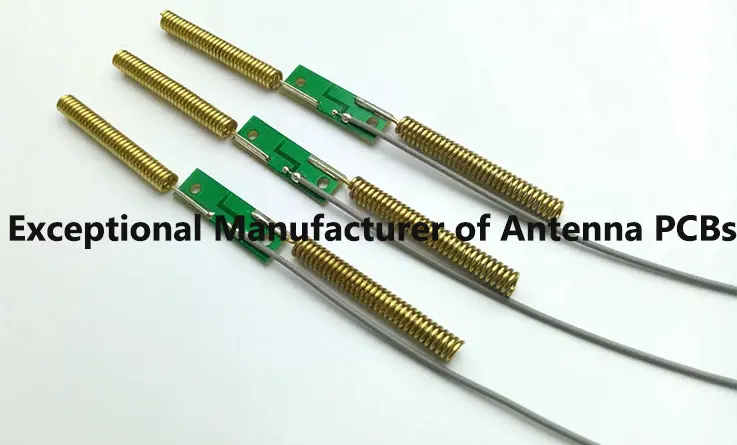
Wire Antennas: These antennas consist of a wire that extends from the printed circuit board into free space. They are designed to have a length that matches a quarter-wavelength over a ground plane and are typically fed using a 50-Ω four transmission line. Wire antennas provide excellent RF range and performance due to their three-dimensional exposure and specific dimensions. Wire antennas can take the form of loops, straight wires, or helix shapes.
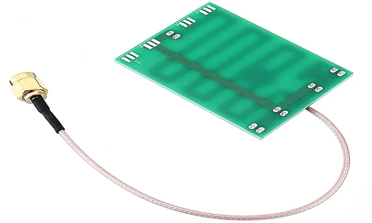
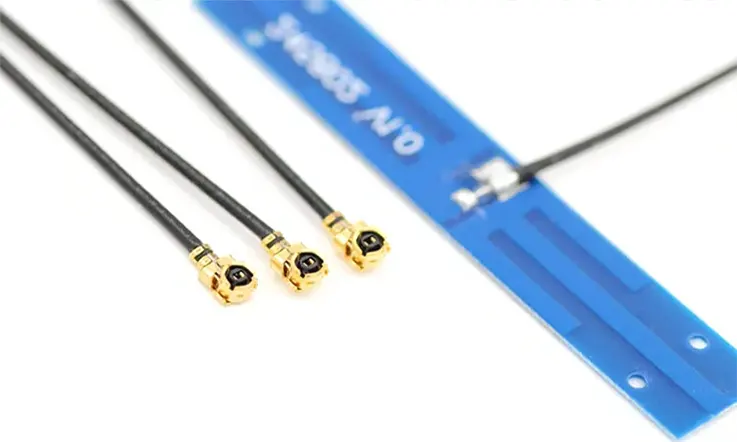
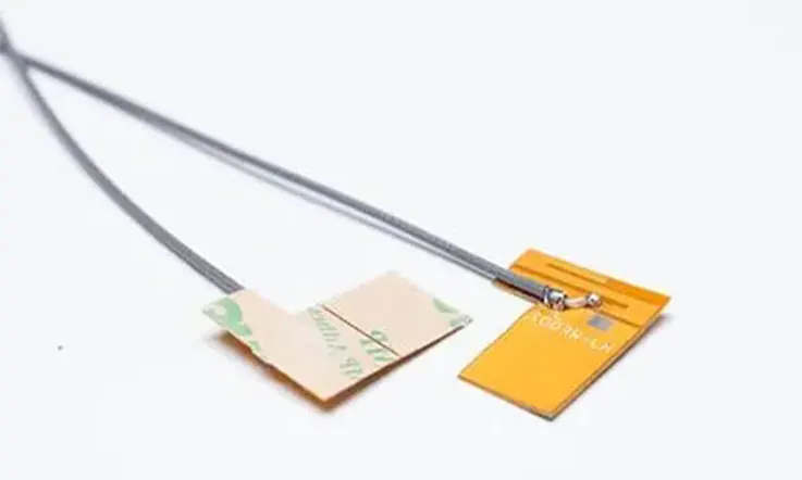
PCB Antennas: Also known as PCB trace antennas, these antennas are created by drawing traces on the printed circuit board. PCB antennas can have various shapes, including meandered traces, straight traces, circular traces, inverted F-type traces, or wiggly curves, depending on the available space and antenna constraints. Unlike wire antennas, PCB antennas are two-dimensional structures within the PCB plane. However, certain guidelines must be followed when converting a 3D antenna into a 2D PCB trace.
PCB antennas provide several advantages such as compact size, lower cost, and ease of manufacturability. However, they generally require more board space and have lower efficiency compared to wire antennas. Despite these limitations, PCB antennas can still offer an acceptable wireless range for Bluetooth Low Energy (BLE) applications.
Chip Antennas: Chip antennas are miniature integrated circuits with a conductor, designed specifically to be used when there is limited space for PCB antenna printing or to support 3D wire antennas. These tiny form-factor antennas are commonly employed in situations where size is a critical factor.
Before starting the design process for an antenna, especially for Bluetooth applications, it is crucial to consider the three main categories of antennas, their fundamental principles, and the different types available within each antenna class.
Understanding the Antenna PCB
Wireless technology has become increasingly prevalent in today’s world, with a wide range of electronic devices, such as smartphones, laptops, and tablets, relying heavily on wireless capabilities. An essential component that enables the transmission and reception of electromagnetic radiation in unrestricted space is the antenna PCB.
The PCB antenna, often found on printed circuit boards, is created by printing copper ink onto the board and establishing an electrical connection with other electronic components like connectors or resistors. This allows the antenna to transmit and receive electromagnetic waves. The antenna PCB plays a crucial role as a wireless device, responsible for the transmission and reception of signals. It finds diverse applications, primarily within the telecommunication sector.
The increasing prominence of 5G technology in the telecommunication sector further emphasizes the importance of antenna circuit boards, as more electronic devices will require these printed circuit boards to facilitate communication, particularly in the context of the Internet of Things (IoT).
Given this context, it becomes essential for electronics designers to have a comprehensive understanding of various aspects of antenna PCBs, specifically focusing on LPWAN (Low Power Wide Area Network) or LoRa PCB antennas. Such knowledge is necessary to effectively design and implement wireless communication systems.
What Is antenna PCB?
An antenna PCB refers to a printed circuit board (PCB) that integrates an antenna within its design. It combines the functionality of a PCB, which provides electrical connections and circuitry, with the capabilities of an antenna, which facilitates wireless communication by transmitting and receiving signals.
The antenna PCB is designed to efficiently radiate or capture electromagnetic waves, allowing devices to establish wireless connections for various applications, such as mobile communication, IoT devices, wireless sensors, and more. By incorporating the antenna directly into the PCB, it offers a compact and integrated solution for wireless communication needs.
Types of Antenna PCB
PCB antennas are integral components of high-frequency PCBs, serving as essential elements for wireless communication. They come in diverse types and are attached to the PCB. Here is a breakdown of the various types of PCB antennas:
Internal PCB Antennas:
Microstrip Antennas: These antenna designs use a metallic trace pattern on the PCB’s surface layer to generate and radiate RF signals.
Patch Antennas: Consisting of a radiating patch structure on the surface of the PCB, they provide low-profile, compact solutions.
Slot Antennas: Utilize slots or gaps in the PCB’s conductive layers to generate electromagnetic waves.
Planar Inverted-F Antennas (PIFAs): Incorporate a compact, meandered or folded element that extends above the PCB surface.
External PCB Antennas:
Monopole Antennas: Consist of a single conducting element extending outwards from the PCB surface, often used in wireless devices.
Dipole Antennas: Comprised of two conducting elements, they are commonly used in radio and Wi-Fi applications.
Yagi-Uda Antennas: Consist of a driven element and multiple parasitic elements arranged in a specific pattern for enhanced directivity.
Planar Antennas:
Planar Inverted-L Antennas (PILAs): Combine a planar conductive strip and a vertical component, forming an L-shaped structure.
Planar Helix Antennas: Utilize a planar spiral structure to create a helical antenna, offering circular polarization.
Slot Planar Antennas: Employ slots cut into the PCB to create radiation patterns and desired impedance characteristics.
Planar Log-Periodic Antennas (PLPAs): Designed with a planar array of radiating elements, covering a wide frequency range.
Integrated Antenna PCBs:
Printed Monopole Array: Consist of multiple monopole antennas arranged in an array to achieve enhanced performance.
Printed Dipole Array: Similar to the printed monopole array, but with multiple dipole antennas arranged in an array configuration.
Specialized Antenna PCBs:
RFID Antennas: Designed specifically for radio frequency identification (RFID) applications, enabling wireless identification and data transfer.
GNSS Antennas: Used for Global Navigation Satellite Systems (GNSS) such as GPS, GLONASS, Galileo, or BeiDou, to receive positioning signals.
It’s important to note that these categories are not exhaustive, and there can be variations and combinations of antenna types depending on specific design requirements and technological advancements.
Factors to Consider When Choosing Antenna PCB Materials
The choice of materials for antenna PCBs depends on several factors, including the desired performance, frequency range, manufacturing process, and cost considerations. Here are some commonly used materials for antenna PCBs:
FR-4: This is the most widely used material for PCBs, including antenna PCBs. It is a flame-resistant epoxy-based laminate that offers good electrical insulation and mechanical strength. FR-4 is cost-effective and suitable for lower-frequency applications.
Rogers: Rogers Corporation is a leading manufacturer of high-frequency laminates specifically designed for RF and microwave applications. These materials provide excellent electrical performance, low dielectric loss, and stable performance at high frequencies. Rogers materials like RT/duroid and RO4000 series are commonly used for antenna PCBs.
Ceramic: Ceramic-based PCB materials, such as alumina (Al2O3) or aluminum nitride (AlN), are known for their excellent thermal conductivity and high-temperature stability. They are often used in high-power and high-frequency applications where heat dissipation and performance stability are critical.
PTFE (Polytetrafluoroethylene): PTFE-based materials, such as Teflon, offer low dielectric constant, low loss tangent, and excellent stability across a wide frequency range. They are commonly used in high-frequency applications, including antennas, due to their low signal loss and consistent performance.
Flexible Materials: For applications where flexibility is required, flexible PCB materials like polyimide (PI) are used. These materials allow the antenna PCB to conform to curved or non-planar surfaces, enabling integration in space-constrained and complex designs.
It’s important to note that the material selection depends on the specific requirements of the antenna design, including frequency range, impedance matching, signal quality, form factor, and cost constraints. Therefore, choosing the right material is crucial to ensure optimal antenna performance and overall system efficiency.
How to Design A Antenna Printed Circuit Boards ?
Designing an antenna printed circuit board (PCB) involves several steps. Here is a simplified outline of the process:
Define antenna requirements: Determine the specifications of your antenna such as frequency, gain, bandwidth, polarization, and form factor.
Choose antenna type: Select the appropriate type of antenna, such as patch antenna, dipole antenna, or helical antenna, based on your requirements and the application.
Determine PCB layout: Decide the size and shape of the PCB layout based on the antenna type and desired performance. Consider factors like ground plane size, clearance from other components, and manufacturing constraints.
Design antenna elements: Use antenna design software or simulation tools to design the antenna elements, such as radiating elements, feed lines, and matching networks. Optimize the design for desired performance metrics.
Incorporate ground plane: Ensure a well-designed ground plane that provides a stable reference for the antenna and minimizes interference.
Optimize impedance matching: Use impedance matching techniques to maximize power transfer between the antenna and RF circuitry. This may involve adding components like baluns, matching networks, or transmission lines.
Test and prototype: Build a prototype of the PCB antenna and conduct tests for performance evaluation. Measure parameters like return loss, radiation patterns, and gain.
Iterative refinement: Based on test results, make adjustments to the design to improve performance. This may involve modifying the antenna geometry, adjusting matching components, or optimizing the ground plane.
Manufacture the PCB: Once the design is finalized, generate the Gerber files or other manufacturing files required for PCB fabrication. Choose a reliable PCB manufacturer to produce the antenna PCB.
Assemble and integrate: Receive the fabricated PCB and assemble it with the required components in the final product or system. Ensure proper mounting and connection of the antenna.
Note that designing antennas can be a complex process and often requires expertise in RF engineering. It may be beneficial to involve an experienced RF engineer or consult specialized resources or literature for more detailed guidance during the design process.
Factors to Consider to Manufacture Antenna PCB
When manufacturing an antenna PCB, several factors need to be considered to ensure the successful production of a high-quality and functional product. Here are some important factors to consider:
Material selection: Choose the appropriate substrate material for your antenna PCB based on factors such as frequency range, dielectric constant, loss tangent, thermal properties, and manufacturing feasibility. Common materials include FR-4, Rogers, or specialty materials designed for high-frequency applications.
PCB stack-up: Determine the layer count and stack-up configuration based on the specific requirements of your antenna design. Consider factors such as signal integrity, impedance control, and isolation between layers to optimize performance.
Copper thickness: Select an appropriate copper thickness for the antenna traces and ground plane based on the desired electrical performance and manufacturing capabilities. Thicker copper layers can provide better signal integrity and heat dissipation.
Antenna placement and clearance: Ensure proper layout and clearance around the antenna components to minimize interference and maintain desired radiation patterns. Consider the proximity of other components, especially those that emit electromagnetic interference (EMI).
Ground plane design: Design an effective ground plane for the antenna to serve as a reference and provide shielding against EMI. Consider factors such as size, shape, and placement to maximize performance and minimize impedance mismatches.
Manufacturing capabilities: Evaluate the manufacturing capabilities of the PCB manufacturer to ensure they can meet your design requirements. Consider factors such as minimum trace width and spacing, minimum drill size, aspect ratio limitations, and other specifications relevant to your antenna design.
Impedance control: Specify tight impedance tolerances for critical transmission lines and impedance-matched areas of the PCB to ensure proper signal integrity and power transfer. This is particularly important for RF and microwave applications.
Surface finish: Choose an appropriate surface finish for the PCB based on your application requirements. Common options include HASL, ENIG, immersion tin, OSP, or silver. Consider factors such as solderability, corrosion resistance, and compatibility with lead-free soldering processes.
Design for manufacturability (DFM): Design the antenna PCB with manufacturability in mind by adhering to industry-standard design rules, avoiding complex or problematic features, and ensuring proper documentation and notes for clarity.
Testing and inspection: Plan for thorough testing and inspection of the manufactured antenna PCBs to verify their functionality and performance. Consider performing tests like continuity testing, RF testing, impedance measurement verification, and visual inspection to ensure quality.
By considering these factors, you can optimize the manufacturing process and increase the likelihood of a successful and reliable antenna PCB. Collaboration with an experienced PCB manufacturer or RF engineer can also provide valuable insights and guidance throughout the manufacturing process.
Challenges and Solutions of Antenna PCBs
In the context of antenna PCB design, some common challenges and potential solutions include:
Miniaturization and Size Constraints:
Challenge: Limited available space for the antenna on the PCB.
Solution: Exploring compact antenna designs such as planar, meandered, or chip antennas. Additionally, employing techniques like fractal or metamaterial structures can help achieve miniaturization.
Bandwidth and Frequency Range:
Challenge: Achieving sufficient bandwidth and covering the desired frequency range.
Solution: Optimizing the antenna geometry, such as using multiple resonant elements, adding matching networks, or incorporating tunable components to enhance the operating bandwidth and frequency range.
Radiation Efficiency:
Challenge: Ensuring a high level of radiation efficiency to maximize the power transmission or reception.
Solution: Careful design considerations, including selecting appropriate materials for the PCB, minimizing losses due to conductor resistivity, utilizing well-matched impedance, and reducing the influence of surrounding components or structures.
Environmental Effects:
Challenge: Antenna performance degradation caused by environmental factors like nearby objects, electromagnetic interference, or varying conditions.
Solution: Conducting extensive EMC/EMI testing to identify potential environmental challenges, employing shielding techniques, adding filters, implementing polarization diversity, or utilizing adaptive algorithms to mitigate the effects of changing conditions.
Manufacturing Considerations:
Challenge: Ensuring manufacturability and consistent performance during production.
Solution: Collaborating with PCB manufacturers to optimize the antenna design for manufacturing processes, considering material properties, fabrication tolerances, and validation testing to ensure consistent performance across production units.
These challenges and solutions provide a glimpse into the considerations involved in antenna PCB design. However, it’s important to note that the specific challenges and solutions can vary depending on the application, frequency range, desired performance, and other project-specific factors.
Future Trends and Developments
Future trends and developments in antenna PCB design are likely to focus on the following areas:
5G and Beyond:
As 5G networks continue to expand and evolve, there will be a need for antenna PCB designs that support higher frequencies, wider bandwidths, and more advanced beamforming and MIMO techniques to enhance data rates and network coverage.
Integrated Multiband Antennas:
With the increasing demand for connected devices operating in multiple frequency bands, there will be a push towards integrated multiband antennas on PCBs. These antennas will allow for simultaneous operation across different wireless standards, such as cellular, Wi-Fi, Bluetooth, and GPS.
Millimeter-wave Antennas:
Millimeter-wave frequencies (above 30 GHz) are being explored for applications like high-speed wireless communication, automotive radar, and imaging systems. Future developments will focus on optimizing antenna designs for these higher frequencies and addressing the challenges associated with propagation characteristics and antenna integration.
Flexible and Wearable Antennas:
Antennas that can conform to irregular surfaces or be integrated into flexible and wearable devices will be a key area of development. This includes using flexible PCB materials, conductive textiles, or printed antenna technologies to enable seamless integration while maintaining performance.
Antenna-in-Package (AiP) Integration:
AiP integration involves embedding antennas within integrated circuit (IC) packages or modules. This approach enhances miniaturization, reduces losses, and improves overall system performance. Future developments will focus on optimizing AiP designs for different applications and integrating multiple functions within a single package.
Advanced Simulation and Design Tools:
The development of more advanced simulation and design tools will enable more accurate modeling and optimization of antenna PCB designs. These tools will consider factors like material properties, non-linear effects, 3D electromagnetic simulations, and optimization algorithms to enhance performance and streamline the design process.
Smart Antenna Systems:
Future antenna PCB designs may incorporate smart antenna systems with advanced signal processing techniques. This includes adaptive beamforming, spatial filtering, and cognitive radio capabilities to dynamically optimize antenna performance in complex wireless environments.
These trends indicate the potential directions for future developments in antenna PCB design, driven by the increasing demand for high-speed wireless communication, IoT devices, smart cities, and emerging technologies like autonomous vehicles and augmented reality.
Conclusion
Antenna PCB design plays a crucial role in enabling wireless communication and connectivity in various devices and systems. The challenges and solutions involved in antenna PCB design include miniaturization and size constraints, achieving sufficient bandwidth and frequency range, ensuring high radiation efficiency, addressing environmental effects, and considering manufacturing considerations.
Antenna PCB design is expected to be driven by trends such as the expansion of 5G and beyond, the integration of multiband antennas, the exploration of millimeter-wave frequencies, the development of flexible and wearable antennas, the integration of antennas within IC packages, the advancement of simulation and design tools, and the adoption of smart antenna systems.
These future trends and developments will contribute to improved wireless connectivity, enhanced performance, and increased functionality in a wide range of devices and applications. As technology continues to evolve, antenna PCB design will continue to play an essential role in enabling seamless communication and connectivity in our increasingly connected world.
Related Posts:
2. JarnisTech – High Quality Bluetooth PCB Manufacturer
3. FAQ Guide About Wireless PCB
4. Why Carrier PCB in Telecommunication Is So Useful?
5. What Is GPS PCB and How to Use GPS Integration into PCB?
6.The Evolution of 5G PCB Technology: Transforming the Telecommunication Industry