In the manufacturing process of printed circuit boards (PCBs), various techniques are employed to shape and refine the blank PCBs before they are ready for component assembly. One such essential step is milling, which involves the removal of excess material from the blank PCB to achieve the desired shape, dimensions, and features. Milling plays a crucial role in PCB fabrication, ensuring precision, accuracy, and functionality of the final product.
By understanding the purpose and advantages of milling blank PCBs, manufacturers, designers, and electronics enthusiasts can gain valuable insights into this critical step, enabling them to make informed decisions and optimize their PCB fabrication processes. So, let’s dive into the details and unravel the significance of milling in PCB manufacturing.
What is Blank PCB?
A blank PCB (Printed Circuit Board) refers to a circuit board that has been manufactured but does not have any electronic components or traces on it. It is essentially a bare board without any circuitry or functionality. Blank PCBs are typically used in the electronics industry as a starting point for designing and creating electronic devices.
The manufacturing process of a blank PCB involves several steps. First, a layer of copper is applied to the board, which serves as the conductive material for the circuitry. Then, a layer of protective material called solder mask is applied to prevent accidental short circuits and to insulate the copper traces. Finally, holes are drilled into the board to facilitate component placement and connection.
Once the blank PCB is ready, it can be used for various purposes. Designers and engineers can mount electronic components such as resistors, capacitors, integrated circuits (ICs), and connectors onto the board to create a functioning electronic device. The components are soldered onto the copper pads and connected using conductive traces on the board, forming the desired circuitry.
Blank PCBs provide a foundation for custom electronic designs, allowing for flexibility and customization in creating specific electronic systems or prototypes. They are commonly used in industries such as consumer electronics, telecommunications, automotive, aerospace, and many others.
Blank PCB Materials
Here are some common blank PCB materials:
FR-4: This is the most common and inexpensive material for PCBs. FR-4 is a composite of woven fiberglass cloth with an epoxy resin binder. It has good mechanical strength and is suitable for most general purpose applications.
CEM-1: Woven cotton paper substrate with epoxy resin. It has better thermal properties than FR-4 but lower mechanical strength. Used for RF and high frequency applications.
Rogers: A variety of high frequency PCB materials by Rogers Corporation with dielectric constants tailored for high speed digital and RF applications. Common Rogers materials include RO4003, RO4350B, RO4835.
Polyimide: Flexible PCB material capable of withstanding high temperatures. Common brands include Kapton and Apical. Used for flexible circuits and rigid-flex boards.
Alumina: Ceramic PCBs with high thermal conductivity used for power circuits and high temperature operation. More expensive than FR-4.
Teflon/PTFE: Woven fiberglass reinforced fluoropolymer with excellent chemical resistance and dielectric properties. Used for high frequency RF boards.
The choice depends on electrical, thermal, mechanical and cost requirements. FR-4 is suitable for most general applications, while more advanced materials are used for specialized high speed or high frequency needs. The PCB fab house can advise on blank material selection.
Blank PCB Color
Blank PCBs typically have a characteristic color that is determined by the base material used for the substrate. The most common color for blank PCBs is typically light yellow or tan. This color comes from the fiberglass-reinforced epoxy resin material (FR-4) that is commonly used for the substrate. FR-4 has a natural yellowish color due to the presence of the fiberglass reinforcement.
While light yellow is the most common color, it’s important to note that blank PCBs can also be found in other colors, such as light green, blue, or even black. These variations in color can be attributed to different formulations of the substrate material or the application of additional coatings or finishes.
It’s worth mentioning that the color of blank PCBs is primarily for aesthetic purposes and does not impact the functionality or performance of the board. The color may vary depending on the manufacturer or specific requirements of the project.
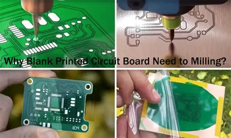
Why Blank PCB Used for Milling?
A blank Printed Circuit Board (PCB) is used for milling because the process involves the mechanical removal of copper layers to create an electrical circuit based on a digital design. This is why the PCB starts as a “blank”, meaning it’s fully coated with a layer of copper on one or both sides.
A few reasons why a blank PCB is used for milling include:
Customization: Milling allows for the creation of highly customized PCB designs. Starting from a blank PCB means that the design can be tailored to the exact specifications of the user.
Rapid Prototyping: If you want to test a design concept quickly, PCB milling is a great option. You can start with a blank PCB, mill your design, and have a functional prototype within a short time.
Cost-Effective for Small Batches: For large-scale production, methods like PCB etching might be more cost-effective. However, for small batches or single boards, milling can be more economical because it doesn’t require the creation of an etching mask.
Reduced Waste: With milling, only the unwanted copper is removed. This could result in less waste compared to methods like etching, where the entire copper layer is first applied and then largely removed.
No Chemicals Required: Unlike etching methods, which use chemicals to remove unwanted copper, milling is a mechanical process that doesn’t require potentially harmful chemicals.
Remember that while milling has its advantages, it also has limitations. It might not be suitable for very complex or high-density PCB designs, and the accuracy is somewhat dependent on the quality of the milling machine used. Each method has its place, and the choice between them depends on the specific requirements of the PCB design project.
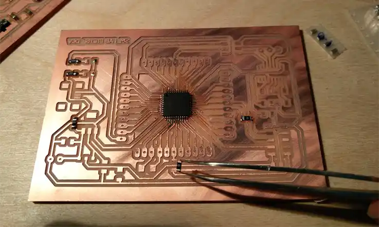
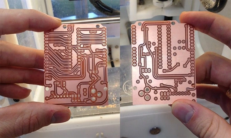
What is Blank PCB Milling?
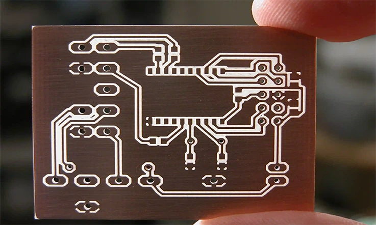
Blank PCB milling is a process for creating custom printed circuit boards (PCBs) by using a computer-controlled milling machine to cut away copper from a blank PCB laminate. It involves the following main steps:
● Design the PCB layout in CAD software and export the Gerber files.
● Secure a blank PCB substrate, usually single or double sided FR-4 or copper clad laminate.
● Align and clamp the blank PCB on the milling machine bed.
● Load the Gerber files into the milling machine software. This converts the PCB layers into toolpaths for the milling bit.
● Perform tool change to load the appropriate end mill cutter. Small end mills are used to carve fine traces.
● Perform surface profiling to account for PCB surface irregularities. This ensures proper depth control.
● Run the milling program which mills away copper from the blank PCB to isolate traces and create pads/vias based on the PCB design files.
● Clean away milling debris and inspect the milled PCB under microscope.
● Post processes like drilling holes, edge plating and solder mask application are done to finish the milled PCB.
Milling provides quicker turnaround time than chemical etching and allows creating fully custom PCBs in a small lab setup. But the equipment cost is higher than etching.
Useful Tips for Blank PCB Milling
Use fine end mills for tracing – Single flute carbide end mills down to 0.1mm work well for PCB traces. Multi-flute end mills are preferred for milling large copper areas.
Minimize runout – Make sure the end mill is tightly secured and has minimal runout. Otherwise it will affect milling quality.
Use sacrificial substrate – Attach a sacrificial fiberglass or acrylic layer on top of the PCB blank during milling. This helps preserve the end mill life.
Optimize feed and speed – The milling feed rate and spindle RPM have to be optimized based on the end mill size to get clean edges. Faster feed and lower RPM for smaller tools.
Use climb milling – Where the cutter rotation opposes the feed direction. It gives better results than conventional milling for PCBs.
Secure PCB blank – Use vacuum hold down or dabs of glue to securely hold the PCB blank in place during milling.
Clear debris – Periodically clear away milling debris using brushes and compressed air to avoid re-cutting.
Limit trace width – Keep trace widths greater than the end mill diameter for cleanest cutting.
Apply solder mask – A solder mask coating will protect the milled traces from oxidation and damage.
Proper fixturing, cutter selection, speeds/feeds and debris control are key to getting good results from PCB milling.
Conclusion
Milling blank PCBs serves multiple purposes and offers significant advantages in the PCB manufacturing process. From achieving precise shapes and dimensions to facilitating component fitment, design flexibility, and signal integrity, milling plays a crucial role in producing high-quality PCBs. It allows for customization, improves thermal management, reduces weight, and optimizes manufacturing costs. By recognizing the purpose and advantages of milling, PCB designers and manufacturers can harness its potential to create superior and reliable electronic products.