
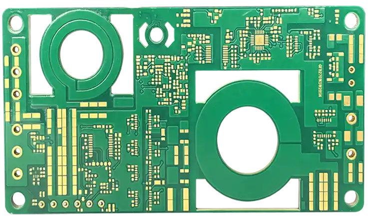
As we exist in an era where electronic devices have become integral facets of our day-to-day existence, the exigency for sophisticated Printed Circuit Board (PCB) technology has escalated. The progression in PCB technology has brought about the emergence of 12 layer PCBs designed to handle the requirements of high frequency and high density connections essential, for todays electronic devices and technologies.
A 12-layer PCB embodies twelve strata of conductive substance, each partitioned by an insulating material, with every layer featuring a distinct array of circuits and components, ultimately forming a comprehensive circuit. In this context, we will further discuss the manufacturing process of 12 layer PCBs, quality control measures, applications, and testing techniques.
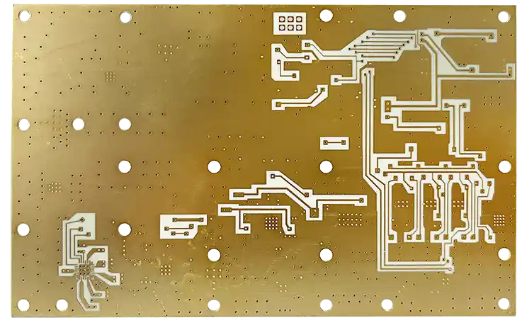
What is 12 Layer Printed Circuit Board?
A 12 Layer PCB denotes a specific class of printed circuit board comprising twelve distinctive conductive material layers isolated by insulating layers. Each layer is characterized by a unique array of circuitry and components, facilitating intricate and high-density circuit designs. With 12 layers of conductive material, these PCBs offer much higher signal density and signal integrity as compared to traditional double-sided or four-layer PCBs.
The extra layers also provide additional flexibility for routing complex high-speed circuits, and the ability to dissipate heat across multiple layers.Therefore, 12-layer PCBs frequently find usage in cutting-edge applications across a multitude of sectors. For example high-speed computing, telecommunications, aerospace and defense, medical instrumentation, automotive systems, and industrial automation.
Design Considerations for 12 Layer PCBs
Here are some design considerations for 12 layer PCBs:
● Stackup Design: It is crucial to design the stackup carefully by considering the material properties, trace and space requirements, impedance control, and signal integrity. The proper stackup design can help to minimize the crosstalk and noise between adjacent layers.
● Controlled Impedance: Since 12 layer PCBs are often designed for high-speed applications, it’s imperative to ensure proper impedance control, which helps to maintain the signal integrity and reduce reflections.
● Power and Ground Planes: Properly designed power and ground planes are critical for reducing EMI/RFI and increasing signal integrity. They also play a vital role in providing stable power delivery to all components of the 12 layer PCB.
● Via Placement: Careful consideration of via placement is necessary to maintain signal integrity and reduce crosstalk and noise. Vias should be placed strategically to avoid coupling between power and signal layers.
● Routing and Trace Widths: Routing and trace widths play an essential role in determining the performance of the 12 layer PCB. The design should consider the signal frequency, impedance, and current capacity when routing and determining trace widths.
● Thermal Management: Adequate thermal management is crucial to avoid overheating and ensure the reliability of the 12 layer PCB. Thermal management includes features such as heat sinks, thermal vias, and copper pours to manage heat dissipation.
Manufacturing Process of 12 Layer PCBs
The production procedure for 12-layer Printed Circuit Boards (PCBs) is a sophisticated, professional knowledge and rich experience. This indispensable process guarantees the ultimate PCB aligns with the essential specifications for operability, dependability, and efficacy. Here is a brief recapitulation of the principal steps implicated in the manufacturing of a 12-layer PCB:
1. Design and Pre-production Planning
●Design: The process begins with the PCB design, using specialized software to layout the circuit schematics, which includes the placement of components, vias, and the detailed layer stack-up.
●Gerber File Generation: Once the design is finalized, Gerber files, which serve as blueprints for each PCB layer, are generated.
●Design Review: A thorough review of the design is conducted to ensure compliance with manufacturing capabilities and to identify any potential issues.
2. Material Selection and Preparation
●Substrate Material Selection: A suitable substrate material, typically FR-4 or a high-performance alternative, is selected based on the application requirements.
●Preparation: Substrate sheets are cut to size and prepped for the layering process.
3. Inner Layer Processing
●Circuit Pattern Transfer: The inner layer circuits are printed onto the substrate using a photoresist and ultraviolet (UV) light exposure.
●Etching: Unwanted copper is chemically etched away, leaving behind the desired circuit patterns.
●Inspection: Automated Optical Inspection (AOI) is used to check the integrity of the circuit patterns.
4. Layer Stacking and Lamination
●Stacking: The inner layers are stacked together with prepreg (fiberglass impregnated with resin) and copper sheets for the outer layers.
●Lamination: The stack is subjected to heat and pressure in a lamination press, bonding the layers into a single, solid board.
5. Drilling and Plating
●Drilling: Holes for vias and component mounts are drilled through the laminated board.
●Plating: The drilled holes are plated with copper to create conductive vias connecting the layers.
6. Outer Layer Processing
●Similar to inner layers, the outer layers are processed to form the required circuit patterns, followed by etching and inspection.
7. Solder Mask Application
●Solder mask is applied to both sides of the PCB, exposing only the areas where soldering will occur, such as pads and vias.
8. Surface Finish
●A surface finish, like HASL (Hot Air Solder Leveling) or ENIG (Electroless Nickel Immersion Gold), is applied to protect the exposed copper and ensure solderability.
9. Silkscreen and Final Inspection
●Component labels and other markings are printed on the PCB.
●A final inspection, including electrical testing, is conducted to ensure the PCB meets all specifications.
10. Routing and Profiling
●The PCBs are routed from the panel and profiled to the required shape and size.
11. Packaging and Shipping
●The finished PCBs are packaged appropriately and shipped to the customer.
This intricate manufacturing process enables the creation of 12-layer PCBs that meet the exacting standards required for advanced electronic applications, providing the necessary circuit density, signal integrity, and mechanical strength.
Quality Control for 12 Layer PCBs
Quality control is essential, in the production of twelve layer printed circuit boards (PCBs) to guarantee that the final product meets high quality standards and fulfills design requirements.
● Dimensional accuracy: The PCB’s dimensions must be precisely measured to ensure they meet the design requirements, including trace widths, spacing, hole diameter, and position.
● Electrical Testing: Electrical testing is performed to verify that the PCB’s tracks, vias, and pads accurately transmit electrical signals between the layers. Advanced testing techniques such as controlled impedance testing may be used to ensure optimum signal performance.
● Visual Examination: The PCB undergoes a visual investigation to identify any possible defects such as indentations, cuts, or disruptions in the trace, gaps in the plating and soldering, along with other aesthetic imperfections.
● Solderability Evaluation: This test involves assessing the solderability of the PCB’s surface through the application of solder paste and its subsequent reflowing.
● Dependability and Robustness Assessment: The PCB is exposed to environmental trials to authenticate its ability to endure the conditions it’s specifically designed for, which encapsulate temperature, humidity, and vibration factors.
● Record-keeping and Traceability: It’s imperative to sustain detailed documentation during the entire process, spanning from design to delivery, encompassing information on materials used, testing parameters, and obtained results. The practice of traceability must be followed to ascertain that any potential issues can be tracked down to their roots.
Advantages of 12 Layer PCBs
12-layer Printed Circuit Boards (PCBs) provide a host of benefits particularly fashioned to align with the demands of intricate and high-performance electronic functions. The advanced design and fabrication competencies needed for these 12-layer PCBs yield inherent characteristics that are favorably appreciated across a diverse range of industries. This includes telecommunications, medical equipment, aerospace, and sophisticated consumer electronic sectors. Below we mention some primary advantages:
●Increased Circuit Compactness
●Enhanced Power Delivery
●Design Versatility
●Improved Reliability
●Suitable for High-Density Applications:
●Reduced EMI/RFI:
●Enhanced Thermal Management
●Improved Signal Integrity
Applications of 12 Layer PCBs
12-layer PCBs are applicated in proceedings that necessitate intricate interconnections and sophisticated routing structure. Herein are some typical instances where 12-layer PCBs find their application:
●Computer Industries
●Communication technology
●Military
●Automation Industries
●Medical equipment
●Automotive technology
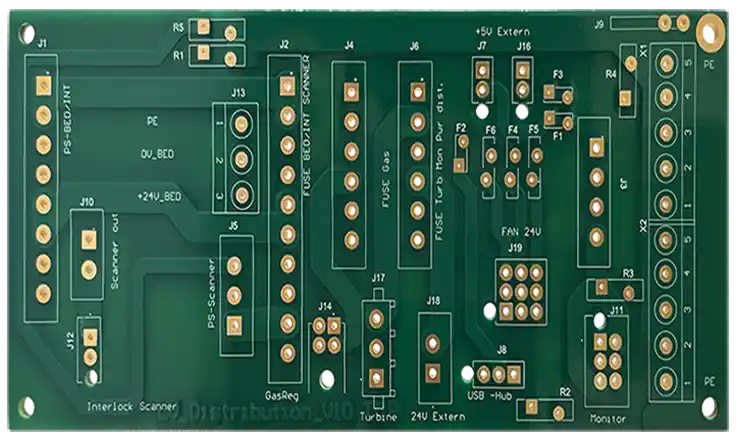
Multilayer PCB manufacturer: JarnisTech (12 Layer PCB)
As a leading producer and supplier of PCB, in China we offer high quality products and services to customers worldwide. Our wide range of customized PCBs includes 12 layer PCBs that feature complex interconnections complex routing structures and excellent signal integrity.
Our 12-layer PCB immediate quotation service guarantees the promptest response time, compelling rates, and unmatched quality, catering to the constantly expanding demands of our clientele. Whether it be a tailor-made PCB design for high-velocity computing, telecommunications or medical apparatus, our expert engineers are equipped to produce innovative and efficient circuit solutions that meet your specifications.
For inquiries regarding 12-layer PCB quotations or immediate pricing, feel free to contact our online customer support or dispatch an email to us. Our team promptly attends to queries and will facilitate your interaction with our technical gurus for a thorough discussion of your stipulations and anticipations.
Technologies on the PCB Manufacturers
| Specifications | Technology | Notes |
| Number of Layers | 1-60 Layers | / |
| PCB Base Materials | Rogers, Shengyi, Nanya, Teflon, Taconic, TUC, ISOLA,Arlon,Nelco, Panasonic,Etc. | We normally keep these materials in stock. If you need a material that is not listed here, please contact us and we can order it for you. |
| Stiffeners | FR4; Polymide; Stainless Steel; Thermo Set and PSA Based Aluminum; Etc… | / |
| Final PCB Thickness | 0.2MM-6MM | / |
| Core Thickness | 1/3OZ-20OZ | / |
| Minimum Line Width/Space | 2.5MIL/2.5Mil | / |
| Minimum Holes Size | 0.10MM | / |
| Surface Finishes | HASL-Leaded Solder; HAS-Lead-Free Solder; Electroless Soft Gold; Wire Bondable Soft Gold; Nickel Flash Gold; Electroless Nickel; Immersion Gold OSP; Electrolytic Nickel /Hard Gold and Selective; Gold; Immersion Silver; Immersion Tin; Carbon Ink; ENIG; | / |
| Silkscreen Colors | White; Black; Yellow Top and Bottom Mix; Red One or Both Sides Mix; Blue; Etc…… | / |
| Ratio of aperture | 12:1 | / |
| Impedance control | +-5%~10% | / |
| Quality / Testing | Inspect to IPC Class 3 Continuity Resistance-10 to 20 Ohms; Net List Test per IPC-356D Isolation Resistance-2 to 30 Megaohms; Test Voltage-100 to 250 Volts Minimum SMT Pitch 0.2 mm; | / |
We are proud to be renowned as a prominent manufacturer of superior 12-layer PCBs in China. Amassing over two decades of experience, we have fortified a commendable repute for delivering specialized, top-tier PCB solutions. At JarnisTech, Our unwavering dedication to perfection is signposted by the array of products we proffer, thereby guaranteeing that we not only cater to but also excel past the diverse needs of our customers, equipped with the most premium 12-layer PCBs at hand.
Our dedication extends to providing unmatched technical and post-sales assistance to our clients. Our profesional cadre of engineers collaborates closely with clients to meet their bespoke needs, furnishing expert recommendations and indispensible insights throughout every phase of the project.
We provide a variety of 12 layer PCB products, such as:
HDI 12 layer PCBs
Standard 12 layer PCBs
rigid 12 layer PCBs
High frequency 12 layer PCBs
Heavy copper 12 layer PCBs
Multilayer PCB with 12 layers
Computer motherboard with a 12 layer PCB
Electronic board with 12 layers
High TG170 FR4 PCB, with 12 layers
Circuit board for a 12 Layer HDI PCB
Immersion Gold Surface on a 12 layer PCB
Why Should You Choose Us?
● We take immense pride in our established status as a dependable and seasoned PCB prototype fabricator, dedicated to offering superior products coupled with unparalleled services to our patrons. Subsequently, our efforts are channelized towards augmenting the efficiency of our manufacturing methods, thus translating into considerable savings in both, time and expenditure, for our clients.
●Through our fast PCB prototype service, we ensure the timely dispatch of printed circuit boards to our clients, strictly adhering to their timeline whilst sustaining quality. Be it a single prototype or an extensive production batch, we possess the capability to meet your demands punctually and within a feasible budget.
● Our minimum orders for PCBs start at just 1 piece, making us a versatile and flexible solution for organizations of all sizes. Our customer support team operates on a 24/7 basis, assuring uninterrupted assistance and guidance throughout the complete journey, spanning from the prototype stage to final delivery.
● We offer a comprehensive one-stop solution for various PCB and SMT stencil production needs, our expert PCB engineers are on-hand for personalized support, ensuring all requirements and specifications are met with precision.
● Quality and reliability are guaranteed when you partner with us. From the PCB quote to the time of delivery, we guarantee top-quality products and services that meet and exceed our customers’ expectations.
● Our advanced production facilities, cutting-edge equipment, and professional personnel collectively empower us to distribute bespoke and top-quality printed circuit boards to a multitude of sectors.
Layer Stack-up Configuration for 10 Layer PCB
The composition of the layer stack-up for a 12-layer PCB is contingent on the specific prerequisites of the application and the design. Generally, a 12-layer PCB constitutes the subsequent layers:
● Top signal layer
● Internal signal layer 1
● Internal ground layer 1
● Internal power layer 1
● Internal signal layer 2
● Internal ground layer 2
● Internal power layer 2
● Internal signal layer 3
● Internal ground layer 3
● Internal power layer 3
● Internal signal layer 4
● Bottom signal layer
This stack-up configuration provides sufficient flexibility for routing complex high-speed circuits and optimal shielding to minimize crosstalk and EMI issues. The internal ground and power layers serve as a reference plane, providing a stable and low-noise ground and power source, respectively. The top and bottom signal layers are utilized for external connections and provide improved signal quality and impedance control.
Nonetheless, the distinct requirements and design objectives of a particular venture could mandate alterations in the layer stack-up arrangement. At JarnisTech, we thoroughly coordinate with our clientele to warrant that their unique needs are accommodated, and we offer expert advice and guidance throughout the design and manufacturing procedures.
Standard 12-Layer PCB Stack Up
The standard 12-layer stack-up is frequently employed and highly favored by PCB designers due to its versatility and adaptability, making it aptly compatible for a range of multilayer PCB applications. Consequently, its appropriateness and practicality designate it as the go-to choice for a multitude of design projects.
The 12-layer stack-up provides ample room for complex and high-speed circuit routing. It offers excellent shielding to minimize interference and EMI issues. The layer stack-up includes internal ground and power planes that provide reference planes for a stable and low-noise ground and power source, respectively.
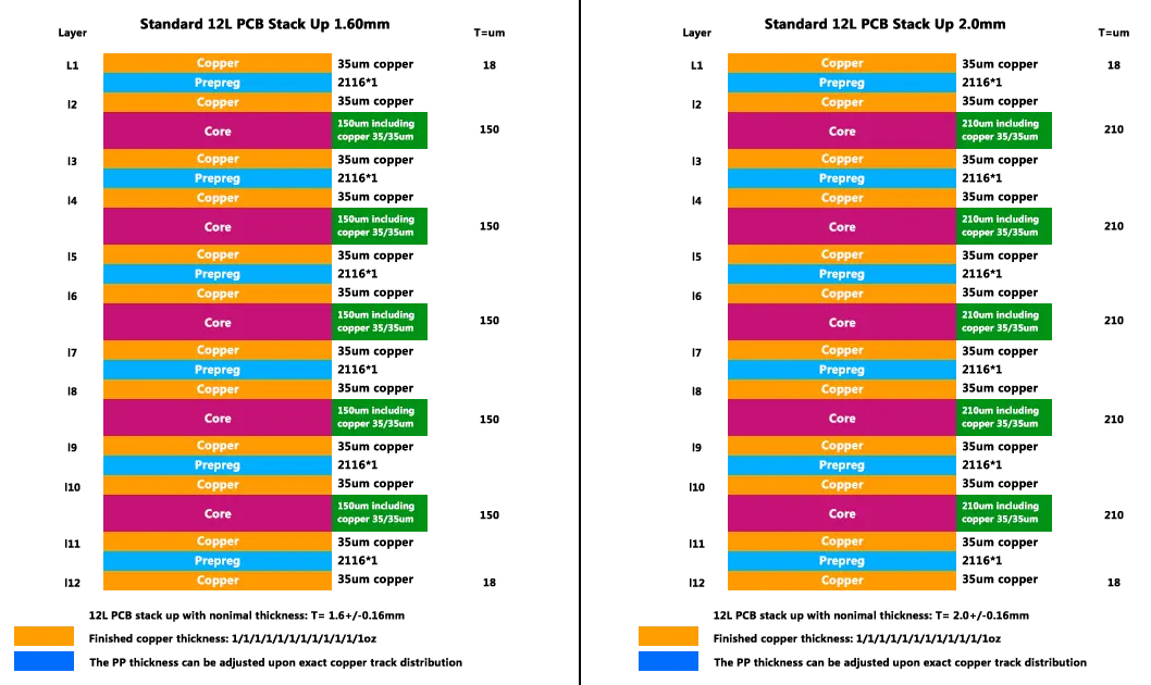
Standard 12L PCB Stacks to 1.6MM Standard PCBs 12L Stacks Up 2.0MM
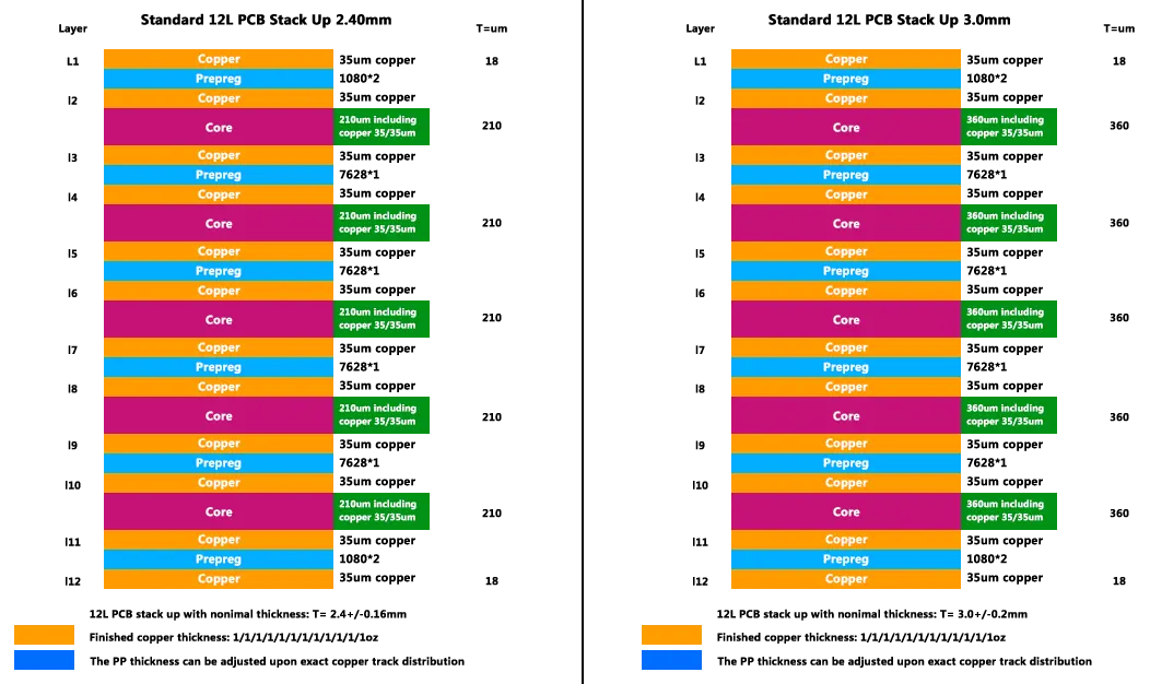
Standard 12L PCB Stacks up wards 2.4MM Standard PCB Stacks Up 3.0MM
JarnisTech offers high-quality 12-layer PCB buildup options that are designed to meet stringent manufacturing standards for quality and price. Our standard 12-layer stack-up configurations provide optimal flexibility and shielding for complex and high-speed circuit routing.
We highly recommend the use of Tg170 Laminate materials for multilayer PCBs with greater than 6-layers to avoid any quality issues during the PCB assembly process, such as delamination of layers and blistering in the lead-free assembly process.
Our choice for a 12 layer PCB stack-up includes copper layers with a thickness of 1 ounce each providing manufacturing capabilities, for intricate multilayer PCBs.
Should you need further specifications, like impedance controls on 12L circuit boards, or if you require PCBs with a 2oz or greater copper layer, we invite you to reach us at [email protected]. Our cadre of seasoned professionals stands ready to guide you through the selection and design stages, assuring that your PCB project perfect finish.
Why Use 12 Layer PCBs?
12 layer PCBs come into play when the circuit design or application prerequisites entail high intricacy and call for the integration of a myriad of components. The employment of 12-layer PCBs can yield advantages such as mitigated noise, superior thermal regulation, and heightened signal integrity.
Furthermore, a 12-layer PCB offers increased routing space, enabling high-speed applications, improved performance, and increased reliability. It bears the capacity to shrink the PCB size by diminishing the required layer count, all the while adhering to the design specifications. In sum, the utilization of a 12-layer PCB emerges as a sensible option for complex and intense applications, where enhanced performance and reliability are critical.
Prototype PCB 12 Layer Delivery Date and Price
As a leading PCB manufacturer, we base our cost estimates on various factors such as process requirements, board size, quantity, and other project details. Clients can submit their project requirements in a Gerber document, and we will provide an accurate cost estimate to meet their budget and project goals.
For general factories, the standard lead time for 12-layer PCB production is typically 13-15 days. However, we understand that fast turnaround times are sometimes essential, which is why we offer expedited production services. With our expedited order option, we can meet our customer’s delivery requirements within a week or less.
At JarnisTech, we are committed to providing reliable and timely PCB production services to meet our clients’ unique needs. Our experienced team is available to provide expert guidance and support throughout the entire process, from initial design to final delivery.
Final Thought
12 layer PCBs are a pivotal element in contemporary electronic design, finding utilization across a multitude of high-density and intricate applications spanning diverse fields. Owing to their enhanced performance capabilities and superior signal integrity, they are often the go-to solution for applications in high-speed computing, telecommunications, aerospace & defense, medical equipment, automotive systems, and industrial automation.
Should you pursue dependable and precise PCBs for your automotive electronic apparatus or other modern electronic devices, 12-layer PCBs make an optimal choice. With their superior stratification, they confer increased adaptability and accommodate more intricate circuit designs and routing.
Here at JarnisTech we are committed, to delivering notch 12 layer PCBs that are reliable and of high quality. As a prominent PCB manufacturer in China, we have a seasoned team of professionals dedicated to crafting robust and long-lasting 12-layer boards compatible with a wide spectrum of contemporary electronic devices. We offer our the best PCBs at prices without compromising on quality standards.
When you choose JarnisTech as your PCB supplier, you can trust that you are receiving the best possible products and services.
PCB Fabrication
Multilayer PCB Manufacturing & Assembly


