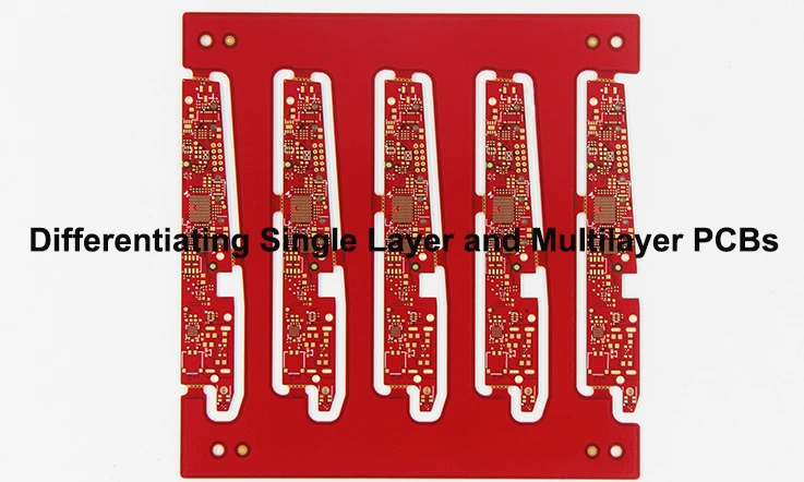
Single Layer PCBs and Multilayer PCBs represent two diverse types of circuit boards, each boasting their unique traits and applications. Understanding the distinct disparities between these two types is critical in choosing the most fitting selection for a specific endeavor. This postprovides a thorough comparative review of Single Layer PCB and Multilayer PCBs, emphasizing their structural differences, design deliberations, performance elements and cost factors.
Definition and Functionality of PCBs
Printed Circuit Board, commonly known as PCB, are integral elements within electrical devices, acting as the bedrock for electrical connectivity and offering mechanical reinforcement for electronic constituents. The fabrication of PCBs involves superimposing layers of insulating substrate materials, typically fiberglass, and overlaying them with pathways made from conductive materials, most often copper. These pathways are etched into the board to facilitate the transport of electrical signals.
The core functionality of PCBs is to offer a framework for affixing and linking electronic constituents, such as resistors, capacitors, and integrated circuits, in a streamlined and orderly fashion. Additionally, they aid in safeguarding against short circuits and offer customization options to align with various application requirements, spanning aspects such as size, form, and functionality.
In essence, PCBs hold a significant position in the functioning of electronic gadgets, offering a dependable and proficient mode for connecting and governing electrical elements. Their utilization spans across a broad spectrum of apparatus, including smartphones, computers, industrial equipment, and automotive systems.
Importance in Electronic Manufacturing
Efficient Assembly: PCB facilitate the accurate and efficient installation and interconnection of electronic components, simplifying the assembly process while diminishing production duration and cost.
Compact Design: PCB enable electronic components to be densely packed together in a compact and organized manner, enhancing the space-effectiveness and portability of electronic devices.
Reliable Connections: PCB offer a dependable and steady medium for interlacing electronic components, considerably reducing the likelihood of unsecured connections, short circuits and other electrical anomalies.
Customization: PCB offer design flexibility tailored to cater to specific needs of a particular usage scenario. It allows for customization in the layouts, dimensions, and operational aspects of the electronic apparatus.
Quality Control: PCB undergo rigorous testing and inspection processes to ensure quality and reliability, helping to maintain consistent performance and durability in electronic devices.
Scalability: The capacity to generate PCB in substantial volumes makes them optimum for extensive-scale electronic manufacturing procedures, thereby facilitating scalability across a diverse array of electronic apparatuses.
Overall, PCB stand as vital constituents in the fabrication process of electronics, providing a solid foundation for the assembly of electronic components and ensuring the efficient and reliable operation of electronic devices.
Definition and Characteristics of Single Layer PCB
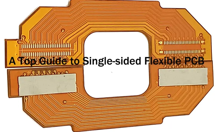
Single layer PCB, commonly known as a single-sided PCB. It is a types of printed circuit board constituted by a single-tier of non-conductive base material (fiberglass or epoxy). It is amalgamated with a conductive layer, predominantly copper, that has been intricately etched on one side of the board. Single sided PCB are commonly employed in less complex electronic devices, where the component count is lower and circuit intricacy is minimal.
Characteristics of single-layer PCBs include:
Simple Design: Single-layer PCBs possess a primary arrangement with elements affixed and interconnected on one side of the board, promoting ease in both manufacturing and assembly processes.
Cost-Effective: Single-layer PCBs are generally more budget-friendly to produce when compared to multi-layer counterparts, making them a preferred option for relatively simpler electronic devices with reduced component counts.
Limited Circuitry: Single-layer PCBs are limited in terms of the circuit’s elaboration and operational ability, owing to the presence of a singular conductive layer dedicated to facilitating electrical signal routes.
Larger Size: Owing to the restricted routing alternatives available on a singular plane, single-layer PCBs may necessitate increased space for organizing traces and components.
Limited Signal Integrity: In comparison to multi-layer PCBs, single-layer ones might exhibit deficits regarding signal integrity and immunity to noise, as there is just one layer available for routing traces and components.
Advantages and Limitations For Single Layer PCB
Single-layer PCBs present particular advantages and constraintslimitations that are pivotal to understand while determining the suitable PCB design for a specific usage. In this section, we will delve into the advantages and limitations with single-layer PCB.
Advantages:
Cost-Effective
Simple Design
Easy to Prototype
Lower Signal Interference
Adequate for Basic Applications
Limitations:
Limited Component Density
Restricted Routing Options
Larger Board Size
Limited Ground and Power Plane Options
Reduced Design Flexibility
Comprehending the advantages and limitations of single-layer PCBs is vital in forming educated choices when selecting the fitting PCB types for a specific project.
Definition and Characteristics of Multilayer PCBs
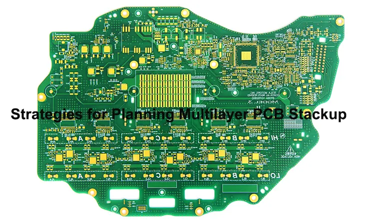
A multi-layer PCB characterizes a circuit board composed of more than two conductive strata, habitually three or exceeding, separated by insulating layers (prepreg) and bonded together with adhesive (core).These conductive layers, also known as copper traces, are interlinked through vias — plated apertures enabling electrical links between varying layers.
Characteristics
Multilayer PCBs possess several distinct characteristics that differentiate them from single layer PCBs. These include:
Increased Design Complexity: Multi-layer PCB supply a heightened scope for design sophistication when compared with single-layer PCB. Extra strata afford a range of routing options, allowing for intricate and compact circuit designs, as well as the incorporation of advanced functionalities.
Higher Component Density: Multilayer PCB can accommodate a higher component density due to the availability of multiple layers for component placement. This facilitates the inclusion of a greater quantum of components, rendering them apt for intricate electronic devices and complex circuitry.
Enhanced Signal Integrity: The use of dedicated power and ground planes in multilayer PCB helps improve signal integrity by reducing noise and providing efficient power distribution. These planes provide a stable reference for signal traces, reducing crosstalk and electromagnetic interference.
Improved EMI/EMC Performance: Multilayer PCBs offer better electromagnetic interference (EMI) and electromagnetic compatibility (EMC) performance compared to single layer PCB. The presence of multiple layers and proper grounding techniques contribute to minimizing EMI emissions and susceptibility to external interference.
Compact Board Size: Multilayer PCBs can achieve the same circuit functionality as single layer PCBs in a smaller physical board size. This compactness is advantageous in applications with space constraints or where miniaturization is a priority.
Enhanced Design Flexibility: Multilayer PCB provide greater design flexibility compared to single layer PCBs. Modifications or additions to the circuitry can be implemented by routing traces on different layers, minimizing the need for major layout changes.
Higher Manufacturing Complexity: Manufacturing multilayer PCBs involves more intricate processes compared to single layer PCB. The lamination of multiple layers, alignment of drilled vias, and proper registration of conductive patterns require advanced manufacturing techniques and equipment.
Increased Cost: Multilayer PCB are generally more expensive to produce compared to single layer PCBs. The additional layers, materials, and manufacturing complexity contribute to higher production costs.
Advantages and Limitations for Multilayer PCBs
When choosing on the PCB desing for a specific use it’s crucial to consider the distinct advantages and Limitations associated with multilayer PCB. Here we’ll delve into the benefit and constraints of using multilayer PCB.
Advantages:
Higher component density
Improved signal integrity
Enhanced performance
Smaller size
Easier routing
Limitations:
Higher cost
Increased complexity
Design limitations
Signal integrity challenges
Heat dissipation
On the whole, the higher component density, elevated performance, and superior signal integrity are advantageous attributes of multilayer PCBs, rendering them apt for intricate electronic apparatuses with rigorous requisites. Nevertheless, they do bear certain limitations such as escalated costs, amplified complexity, and probable signal integrity issues that require meticulous attention throughout the design and manufacturing phases.
Key Differences between Single Layer and Multilayer PCBs
Single-layer and multilayer PCB possess unique attributes that distinguish them. Gaining insight into the essential disparities between these two categories of PCB is imperative for choosing the optimal types for a particular application. Let’s consider their key differences:
Structure and Layer Count:
●Single Layer PCB: Single layer PCB consist of a single conductive stratum, generally composed of copper, sandwiched between two insulating layers (substrate). These pcb board referred to as single sided PCB.
●Multilayer PCB: It’s consist of multiple conductive layers, typically three or more, separated by insulating layers (prepreg). The layers are bonded together with adhesive (core) and interconnected through vias.
Design Complexity and Flexibility:
●Single Layer PCB: Single layer PCB have a simpler design with limited routing options. They are suitable for basic circuitry and applications with straightforward requirements.
●Multilayer PCB: Multilayer PCB offer higher design complexity and greater flexibility. These PCB board allow for intricate circuit designs, advanced functionalities and the integration of diverse components.
Component Density:
●Single Layer PCB: Single layer PCB have limited space for component placement due to their single conductive layer. these PCB board suitable for applications with fewer components and simpler layouts.
●Multi layer PCB: Multilayer PCB can accommodate a higher component density due to the availability of multiple layers. This makes them suitable for complex electronic devices and advanced circuitry.
Signal Integrity and EMI/EMC Performance:
●Single Layer PCB: Single layer PCB may be more susceptible to signal interference and electromagnetic interference due to longer trace lengths and limited grounding options.
●Multilay er PCB: Multilayer PCBs provide superior signal integrity andimproved EMI/EMC performance. By designating specific planes for power and grounding in a multilayer PCB, noise reduction as well as the minimization of crosstalk and EMI releases is achieved.
Board Size and Compactness:
●Single Layer PCB: Accommodating the same circuit functionality as a multilayer PCB may require a larger physical board size for a single layer PCB.
●Multilayer PCB: With their capability to incorporate the same circuit functionality as single-layer PCBs within a more compact board size, multilayer PCBs reveal their advantage in applications where spatial limitations exist or when downsizing holds significance.
Manufacturing Complexity and Cost:
●Single Layer PCB: Single layer PCB involve simpler manufacturing processes and generally have lower production costs compared to multi layer PCB.
●Multi layer PCB: Multilayer PCB involve more complex manufacturing processes due to the lamination of multiple layers and require advanced techniques and equipment. Therefore, elevating their production cost.
Repair and Maintenance:
●Single Layer PCB: Single layer PCBs are relatively easier to repair and maintain since all components and traces are accessible from one side.
●Multi layer PCB: Repairing specific layers within a multilayer PCB can be challenging and may require specialized tools and expertise.
Factors Influencing the Choice of PCB Type
In selecting the suitable PCB types for a definite application, numerous factors are instrumental. The decision depends on a spectrum of contemplations tied to the necessities and limitations of the project. Here are a few primary elements that impact the selection of the PCB type:
1.Complexity of the circuit:
The intricacy of the circuit design is a substantial in the selection of the PCB types. Multilayer PCB are more fitting for sophisticated circuits with heightened component density, whereas single-layer PCB are more suitable for less complicated circuits.
2.Performance requirements:
The performance requirements of the electronic device, such as signal integrity, immunity to noise, and high-frequency operation, are vital parameters in the decision of the PCB types. Multilayer PCBs are typically zoned for applications demanding advanced performance and sophisticated capabilities.
3.Size constraints:
The dimensional limitations of the electronic apparatus have a bearing on the selection of PCB type. Multilayer PCBs are capable of achieving a diminutive form factor in comparison to single-layer PCBs, rendering them perfect for compact devices where spatial availability is restricted.
4.Cost considerations:
Cost considerations play a notable role in determining the type of PCB to be utilized, Since that the manufacturing process of multilayer PCB accrues more costs in comparison to their single-layer counterparts. Cost constraints may prompt the decision to opt for a more economical and simpler single-layer PCB.
5.Manufacturing and assembly complexity:
The intricacy involved in the fabrication and assembly of the PCB figures prominently in the selection of the PCB type. Multilayer PCB necessitate more sophisticated manufacturing techniques and know-how, whereas the production of single-layer PCB is comparatively simpler and expedited.
6.Signal integrity requirements:
The requisites for signal integrity in the electronic apparatus, including control impedance, signal reflections and crosstalk, carry weight in determining the PCB type. Multilayer PCBs provide superior signal integrity relative to single-layer PCBs, thus making them fitting for high-frequency applications.
7.Thermal management needs:
Thermal management needs and heat transfer requirements bear upon the selection of PCB type. Owing to their structure laden with numerous conductive layers, multilayer PCBs may pose hurdles concerning heat challenges, thereby necessitating additional thermal management solutions.
Conclusion
The select between Single Layer PCBs and Multilayer PCBs is influenced by numerous elements such as the intricacy of the circuit, size limitations, signal integrity needs, cost aspects, manufacturing complexity, reparability, and time restrictions. Single Layer PCBs are appropriate for uncomplicated circuits, more constrained budgets, and simpler repairs, while Multilayer PCBs bring benefits in the form of design flexibility, component density, signal integrity, EMI/EMC performance, and compact size. By judiciously assessing these aspects, one can make a studied decision to guarantee the most advantageous PCB types is selected for their precise application.
For OEMs that specialize in creating mechanical products needing digitization, it’s vital to foster collaboration with a trustworthy and adept PCB assembly services provider. It is imperative to thoroughly communicate your specific requirements to ensure the production of the appropriate PCBA that aligns with your needs.
JarnisTech is a versed PCB producer and a PCB assembly services supplier equipped with state-of-the-art PCBA abilities, offering thorough all-inclusive services. Additionally, our corporation has expertise in manufacturing a range of complex cable and wire harness assemblies, such as ribbon, coaxial, and fiber optic assemblies, as well as custom cable harnesses.
Our services
Multilayer PCB Manufacturing & Assembly

