
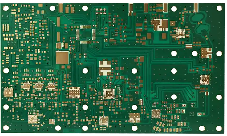
20-layer PCBs are revolutionizing the way electronic devices operate. Gone are the days of traditional two-layer designs. Today, with the growing demand for high-performance, miniaturized, and highly complex devices, 20-layer PCBs have emerged as an innovative solution to meet these needs. A 20-layer PCB allows us to fit multiple signals, power planes, and grounding planes into a single board, offering unparalleled performance in a small package.
In this guide, you’ll discover detailed insights into the design and layout processes, the materials and tools that bring these circuit boards to life, and the steps involved in manufacturing and assembly.
Introduction to 20-Layer PCB Technology
As electronics continue to evolve and the demand for high-performance devices grows, the need for efficient and high-capacity circuit boards is on the rise. One such solution that has become increasingly popular in industries like wearables, medical devices, and aerospace is the 20-layer PCB. These advanced designs are capable of handling complex systems that require high-speed signal transmission, efficient power distribution, and minimal interference.
In this section, we’ll explore the fundamentals of 20-layer PCB technology, from its basic structure to its applications across various industries. Therefore, if you’re a designer, manufacturer, or engineer, understanding the nuances of 20-layer PCBs will give you the edge you need to create cutting-edge electronics.
What is a 20-Layer PCB?
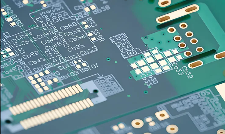
A 20-layer PCB is a multi-layered circuit board consisting of 20 layers, including conductive layers, insulating layers, and dielectric materials. These layers are stacked together to create a highly compact, high-performance circuit board capable of handling complex designs. The layers are strategically arranged to facilitate high-speed signal transmission, efficient power distribution, and to reduce noise.
The benefits of a 20-layer PCB include enhanced signal integrity, reduced interference, and improved reliability. These advantages make 20-layer PCBs ideal for demanding applications where space is limited, but performance is non-negotiable.
Table 1: Layer Breakdown of a 20-Layer PCB
| Layer Type | Function | Typical Material |
| Signal Layers | Carries data and communication signals | Copper |
| Power Planes | Distributes power across the board | Copper or internal planes |
| Ground Planes | Reduces noise and enhances stability | Copper |
| Prepreg Layers | Insulates and separates the conductive layers | Resin-based prepreg |
| Copper Layers | Provides electrical conduction | Copper |
By using these layers in combination, the PCB can carry out multiple functions like power distribution, signal processing, and grounding. In this way, the 20-layer design allows for high-density interconnects, offering performance benefits without compromising on space.
The History and Evolution of 20-Layer PCBs
The evolution of multi-layer PCB technology began with basic single-layer designs and slowly progressed as human found ways to increase the density and complexity of circuits. As early designs became less feasible for modern devices, the demand for multi-layer PCBs grew. This led to the creation of 2, 4, 6, and eventually 20-layer boards.
The development of the 20-layer PCB represented a major advancement in circuit board design. These boards enabled more efficient signal routing, better power distribution, and reduced electromagnetic interference (EMI), addressing the growing complexity of electronics.
The rise of advanced technologies such as 5G, high-speed computing, and miniaturized devices further drove the need for high-performance boards, and the 20-layer PCB was well-suited to meet these requirements.
Table 2: Key Milestones in PCB Evolution
| Year | Advancement | Key Benefit |
| 1970s | Single-layer PCB introduced | Simple designs for early electronics |
| 1980s | Multi-layer PCB technology developed | More complex circuits, higher performance |
| 1990s | 4-6 layer PCBs became mainstream | Space-saving, higher-density applications |
| 2000s | 20-layer PCBs introduced | Allows complex, high-performance designs |
| 2020s | Widespread adoption in wearables, 5G, aerospace | Handling high-speed signals and miniaturization |
This progression showcases how the 20-layer PCB was created as a response to the increasing need for more sophisticated electronics. Its ability to handle high-frequency signals and fit into compact designs has made it the preferred option for modern devices, especially those in main sectors.
Why Choose a 20-Layer PCB?
Choosing a 20-layer PCB offers a range of advantages, particularly when you’re dealing with high-density interconnect (HDI) designs that require intricate, compact layouts. The extra layers provide more space for routing, signal processing, and power distribution, which is essential for devices with many components.
Industries such as medical devices, aerospace, and wearables can benefit significantly from the high-density design offered by a 20-layer PCB. These industries demand high-performance systems where space is at a premium, and performance cannot be compromised. A 20-layer PCB allows for better signal routing, power efficiency, and overall system reliability, making it a preferred choice for us.
Table 3: Industries Benefiting from 20-Layer PCBs
| Industry | Key Benefit of 20-Layer PCBs | Example Application |
| Wearable Technology | High-density signal routing and miniaturization | Smartwatches, fitness trackers |
| Medical Devices | Stable signal processing and power distribution | Portable diagnostic tools |
| Aerospace & Defense | Durability, high reliability under harsh conditions | Satellites, military electronics |
| Telecommunications | High-speed signal transmission | 5G infrastructure |
In these industries, the benefits of having multiple layers in a compact form can lead to improved product designs that can withstand demanding environments while offering superior functionality. By choosing a 20-layer PCB, we can reduce the need for complex interconnections and eliminate the challenges of traditional single-layer boards.
PCB Design Software for 20-Layer PCB Projects
Designing a 20-layer PCB demands precision and the proper tools to handle the complexities of a high-density multi-layer board. From the initial layout to simulation and manufacturing prep, the software you choose has a big impact on the success of the project. Advanced EDA PCB design tools like Altium Designer, KiCad, and Eagle help engineers craft detailed layouts that not only fulfill functional requirements but also ensure manufacturability.
These tools offer features like signal integrity analysis, thermal management simulations, and 3D visualizations, all of which are highly useful when designing 20-layer PCBs. Let’s explore how these tools can streamline and enhance your design process.
Best PCB Design Tools for 20-Layer PCB Layout
When it comes to designing a 20-layer PCB, the choice of PCB design software can significantly affect the efficiency and accuracy of the layout process. Some of the top tools for 20-layer PCB design include Altium Designer, KiCad, and Eagle.
●Altium Designer: Known for its user-friendly interface and powerful features, Altium Designer supports multi-layer PCB design and integrates seamlessly with manufacturing processes. It comes equipped with real-time 3D visualization, which helps in understanding the complex interconnections within a 20-layer PCB. Its ability to automate routing and provide comprehensive design checks makes it a favorite among experienced engineers.
●KiCad: This free, open-source tool is an excellent choice for those looking to design 20-layer PCBs without the hefty price tag. KiCad supports multi-layer design and offers features like a built-in schematic editor and PCB layout editor. It’s a great choice for engineers working with a tight budget but still needing high-quality designs.
●Eagle: Eagle provides an intuitive design environment and comes with a host of powerful features for PCB layout. It’s better for users who need to design multi-layer boards and need high-level control over design rules and constraints.
Simulation Tools for Signal and Thermal Integrity in 20-Layer PCBs
As 20-layer PCBs increase in complexity, it becomes more difficult to manage signal integrity and thermal performance. Simulation tools help ensure that signals remain consistent across all layers and that the board can properly manage heat dissipation from high-power components.
●Signal Integrity Simulation: Signal integrity is a primary concern when designing high-density 20-layer PCBs. Tools like Altium Designer and Cadence Allegro provide simulations to check for any potential signal degradation, such as crosstalk or noise interference, which can arise from closely packed traces in multi-layer designs. By analyzing the impedance, reflection, and transmission delay in the simulation phase, we can prevent these issues from making it to the manufacturing stage.
●Thermal Simulation: Managing heat dissipation is a core aspect of high-density designs like 20-layer PCBs.. Simulation tools allow for real-time analysis of how heat flows through the layers and how efficiently the PCB can dissipate it. Software like ANSYS Icepak or Mentor Graphics performs thermal simulation, helping us optimize the PCB’s layout for better heat distribution, reducing the likelihood of thermal damage during operation.
Managing Design Complexity with 20-Layer PCB Software Features
Designing 20-layer PCBs is no small feat, and managing the complexity requires specialized software features that help us navigate the intricacies of multi-layer boards. These PCB design tools come equipped with a variety of features that simplify the process and help manage design constraints more effectively.
●Layer Stack Management: Advanced PCB software like Altium Designer allows for easy configuration of the layer stack-up, ensuring that the signal layers, power planes, and ground layers are properly configured. For 20-layer PCBs, the ability to visualize and modify the stack-up directly within the software ensures that the design is optimized for both performance and manufacturability.
●Design Rule Checks (DRC): For a 20-layer PCB design, adhering to strict design rules is essential to avoid errors during manufacturing. PCB design software offers automated design rule checks (DRC) that flag any potential violations of spacing, trace width, or other constraints that could hinder the functionality or manufacturability of the board.
●3D Visualization: With the complexity of 20-layer PCBs, having the ability to visualize the entire design in 3D is a huge advantage. Tools like Altium Designer offer a real-time 3D view of the design, which allows us to identify potential issues in the board stack-up, trace routing, and component placement, reducing the chances of making costly mistakes during production.
Key Design Considerations for 20-Layer PCBs
Designing a 20-layer PCB requires a methodical approach. Each layer plays a role, and their arrangement can directly impact the performance, reliability, and functionality of the final product. Unlike simpler designs, 20-layer PCBs present unique challenges due to the density of interconnections, signal integrity concerns, and the need for effective power distribution.
In this section, we’ll examine some of main considerations that need to be addressed when designing a 20-layer PCB. From how the stack-up is structured to techniques for managing signal integrity and handling power distribution, we will discuss how to ensure your design performs as expected. So, if you’re working on aerospace electronics, medical devices, or high-speed communication systems, these considerations will help refine your PCB design to meet the demands of these applications.
Understanding the 20-Layer PCB Stack-Up Structure
The stack-up design of a 20-layer PCB influences how the layers interact with one another. Careful layer arrangement helps optimize space usage while maintaining the board’s performance and reliability. A well-organized stack-up supports efficient signal routing, consistent power distribution, and reduces interference between layers.
Typically, a 20-layer PCB includes signal layers, power planes, and ground planes. Signal layers are used for routing the electrical connections between components. Power planes distribute power evenly across the circuit, and ground planes provide a stable reference. Between these conductive layers, there are insulating layers made of prepreg, a resin-based material that separates the layers and prevents shorts.
Table 1: Example of 20-Layer PCB Stack-Up Configuration
| Layer Number | Layer Type | Function |
| 1, 2 | Signal Layers | Carries high-speed signals |
| 3, 4 | Power Plane | Distributes power to the circuit components |
| 5, 6 | Ground Plane | Provides grounding for the entire PCB |
| 7-16 | Signal Layers | High-speed signal routing |
| 17, 18 | Power Plane | Ensures stable voltage distribution |
| 19, 20 | Ground Plane | Additional grounding for noise reduction |
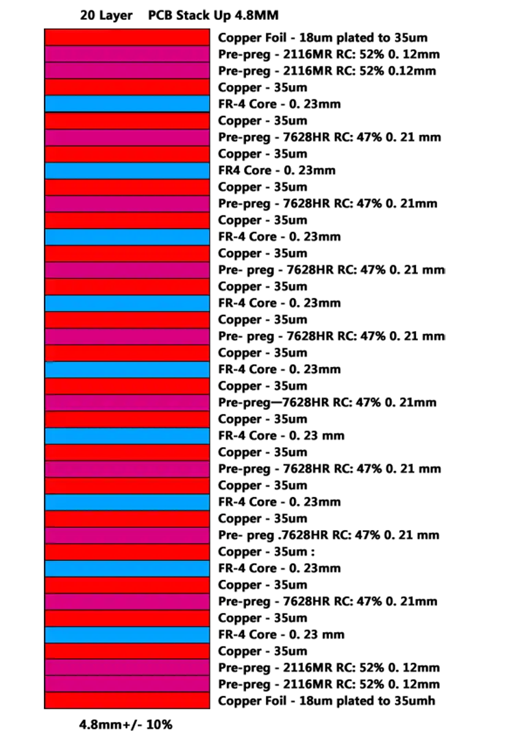
Substrate 20 Layer PCB 4.8mm+/-10%
In this configuration, it’s common for power and ground planes to be alternated with signal layers. This method not only improves performance but also reduces the risks of electromagnetic interference (EMI) and improves thermal management, especially in high-density designs.
Signal Integrity and Impedance Control in 20-Layer PCBs
Signal integrity can make or break the success of a 20-layer PCB, particularly in high-speed applications like 5G or wearable devices. High-frequency signals need to be managed properly to avoid reflections, crosstalk, and signal degradation. To achieve this, signal traces must be carefully routed, and impedance must be controlled across the PCB.
Impedance control ensures that signals travel along the PCB traces without interference. If the impedance of the trace is not controlled, signal distortion can occur, leading to errors in data transmission. For high-speed designs, controlled-impedance traces are used to maintain a uniform impedance throughout the circuit. These traces are carefully calculated based on the width of the trace, the distance from the ground plane, and the material used for the PCB.
Table 2: Example of Impedance Control Techniques in 20-Layer PCB
| Impedance Type | Trace Width | Material Used | Purpose |
| Controlled Impedance | 5 mils | FR4 or Rogers PCB Material | Prevent signal reflection and maintain stability |
| Differential Impedance | 6 mils | Rogers, Teflon, or PTFE | Used for high-speed differential pairs, ensuring balanced signal transmission |
| Microstrip Impedance | 4 mils | Standard PCB material | Reduces signal loss by maintaining a uniform impedance level across the trace |
With controlled impedance, the PCB can handle faster data transmission speeds while minimizing signal loss. This is a common practice for designs that require high-speed communication, like in telecommunications or medical equipment.
Power Distribution and Grounding in Multi-Layer PCBs
Power distribution and grounding are often overlooked during the design process but are essential for ensuring a stable and efficient system. In a 20-layer PCB, power planes and ground planes are used to ensure that power is distributed evenly across the board and that noise is minimized.
The power planes supply the necessary voltage to components, while the ground planes provide a stable reference for the signals. Proper grounding also helps with reducing the impact of external noise sources, which can affect signal quality. The arrangement of power and ground planes in a multi-layer design ensures that the electrical performance remains consistent even when the board is handling high currents.
Table 3: Example of Power Distribution in 20-Layer PCBs
| Layer Number | Plane Type | Voltage Level | Purpose |
| 3, 4 | Power Plane | 3.3V / 5V | Supplies power to the active components |
| 5, 6 | Ground Plane | 0V | Provides a stable ground reference to minimize noise |
| 17, 18 | Power Plane | 12V / 15V | Dedicated power for high-power components like sensors |
| 19, 20 | Ground Plane | 0V | Ensures complete grounding across the PCB |
The use of power and ground planes helps to reduce the possibility of voltage drops and ensures the stability of the entire system. By minimizing power loss and controlling noise, the board operates at its full potential, even in complex, high-density applications.
Advanced Manufacturing Techniques for 20-Layer PCBs
When it comes to manufacturing 20-layer PCBs, the complexity of the design and the precision required for its fabrication cannot be overstated. With each additional layer, the design challenges multiply, requiring specialized techniques and materials to maintain integrity. Whether it’s ensuring high-frequency performance, managing signal integrity, or optimizing heat dissipation, advanced manufacturing techniques are core to creating reliable, high-performing 20-layer PCBs.
In this section, we’ll break down the best practices, materials, and technologies that ensure the efficient production of multi-layered PCBs. Let’s dive into the methods that transform your concept into a fully functional board ready for production.
Selecting the Right Materials for 20-Layer PCBs
Choosing the right materials for 20-layer PCBs is like picking the perfect ingredients for a gourmet meal—get it right, and the results will be smooth sailing. The material chosen for the PCB must align with the performance requirements of the final product, which is why we need to dig deeper into the most suitable materials for high-performance boards.
PCB Materials: More than Just a Surface-
The right substrate material ensures the long-term stability of the PCB, especially in high-density and high-frequency designs. Here’s where materials like Rogers PCB, Shengyi PCB, and Taconic PCB shine, offering not just electrical performance but also mechanical reliability across various environments.
1.Rogers PCB: Rogers offers excellent performance for high-frequency and high-speed applications. Its low loss and stable dielectric properties make it ideal for RF, telecommunications, and even automotive applications where precision is everything. With materials like RO4000 and RO3000 series, you can expect consistent signal transmission, which is a must in main designs.
2.Shengyi PCB: Known for its high-temperature resistance and good electrical properties, Shengyi PCB materials are widely used in automotive, industrial, and consumer electronics applications. The materials are especially well-suited for designs that require durability and stable performance under varying temperatures.
3.Taconic PCB: When you’re looking for a material that holds up under pressure—whether in aerospace, medical devices, or defense applications—Taconic is a go-to choice. Its high-frequency and low-loss properties make it suitable for high-speed designs where precision and reliability are non-negotiable.
Other materials like Isola, Nelco, and Teflon PCB further bolster the material pool, offering tailored solutions for everything from aerospace to high-speed networking. Therefore, no matter what your specific application is, the right material can make a world of difference in the performance and longevity of your 20-layer PCB.
Table 1: PCB Materials for 20-Layer PCBs
| Material | Applications | Key Features |
| Rogers PCB | RF, telecommunications, automotive | Low loss, high-frequency performance |
| Shengyi PCB | Automotive, industrial electronics | High temperature resistance, stable dielectric |
| Taconic PCB | Aerospace, medical, high-speed communications | Excellent high-frequency stability |
| Isola PCB | Consumer electronics, networking | High-speed signals, low loss |
| Nelco PCB | 5G, aerospace, RF | Stable at high frequencies, strong mechanical properties |
| Teflon PCB | Aerospace, medical, high-speed communication | Low dielectric loss, high-frequency stability |
The material selection process isn’t just about picking what’s available—it’s about choosing the material that will give your design the edge it needs to perform in demanding environments.
Microvia and HDI Technology in 20-Layer PCB Production
As designs become more compact and the demand for high-performance PCBs increases, technologies like Microvia and HDI (High-Density Interconnect) have become the backbone of high-layer PCBs. These techniques allow manufacturers to pack more functionality into the same space, resulting in denser, more efficient designs.
Microvias and HDI Technology: The Heart of Dense PCB Designs-
●Microvia technology is central to the production of high-density, multi-layer PCBs. Microvias are tiny vias that connect the inner layers of a PCB without the need for traditional, large through-holes. These tiny holes can be as small as 75 microns in diameter, allowing for increased routing space and reducing signal loss and interference. This makes them particularly useful in 20-layer PCBs where maintaining signal integrity is a top priority.
●HDI technology takes things a step further. By utilizing smaller vias and tighter trace routing, HDI PCBs are capable of achieving a higher layer count with more densely packed circuits. This technology is commonly used in mobile devices, medical equipment, and other applications where board space is limited, but performance cannot be compromised.
Both Microvia and HDI technology are integral to producing 20-layer PCBs with high-density interconnects, allowing for smaller, faster, and more efficient designs. In addition to via-in-pad designs, these technologies enable us to achieve complex, multilayered boards that can handle high-frequency signals and more complex routing without the performance hits that come with traditional through-hole methods.
The 20-Layer PCB Fabrication Process: Key Steps
Fabricating a 20-layer PCB is not for the faint of heart. From lamination to etching, drilling, and plating, each step in the process requires precise attention to detail to ensure the finished product meets both electrical and mechanical requirements.
Step-by-Step: Crafting the Perfect 20-Layer PCB-
1.Lamination: In this process, each layer of the PCB is fused using heat and pressure, assembling the 20-layer PCB stack-up. Proper alignment during this stage is necessary—misalignment can lead to signal integrity problems, which you’ll want to prevent.
2.Etching: Once the layers are laminated, the next step is etching. This is where the copper traces are defined, and your circuit paths begin to take shape. At this stage, the precision of your etching process dictates the overall quality of the design. High-density boards require extremely fine trace widths, which only high-quality etching systems can achieve.
3.Via Drilling and Plating: Drilling microvias or traditional vias into the PCB allows for electrical connections between layers. This step involves using laser drills or mechanical drills, depending on the via type. After drilling, the vias are plated to form electrical connections between layers. HDI and via-in-pad technologies further streamline this process for more complex designs.
4.Testing and Inspection: After fabrication, extensive testing and inspection are done to ensure the PCB meets the required standards. Whether it’s visual inspection, X-ray inspection for internal layer connections, or electrical testing, ensuring the board’s quality before moving to the next stage is a must.
Overcoming Challenges in 20-Layer PCB Design and Manufacturing
Designing and manufacturing 20-layer PCBs requires precision and attention to detail—there’s no room for cutting corners. As more layers are added, the complexity increases, introducing challenges in manufacturability, heat management, and reliability. However, this is where the opportunity lies. The path to success in designing these multi-layer boards is in recognizing the challenges and knowing how to navigate them.
In this section, we’ll explore the common challenges faced during the design and manufacturing of 20-layer PCBs, and we’ll dive into effective strategies to overcome them.
Design for Manufacturability (DFM) in 20-Layer PCBs
When you’re dealing with high-layer count PCBs, Design for Manufacturability (DFM) is not a suggestion—it’s a necessity. The more complex the design, the harder it becomes to manufacture. Let’s face it, a beautifully designed PCB that’s impossible or inefficient to produce is nothing more than a theoretical concept. So, how do you ensure that your 20-layer PCB design is optimized for manufacturability? You need to take a deep dive into the details and make sure your design is as streamlined as possible for the production process.
DFM: Reducing Production Costs and Avoiding Pitfalls-
By adhering to DFM principles, you’re setting yourself up for a smoother, cost-effective manufacturing process. One of the first things to consider is layer stack-up. Properly managing the 20-layer PCB stack-up ensures not only signal integrity but also optimal electrical performance. Overly complex routing that crosses too many layers can lead to errors during manufacturing. By simplifying the routing wherever possible and avoiding unnecessary vias, you’re making life easier for the manufacturer and reducing the chances of production delays.
Another DFM best practice is optimizing your via design. For instance, microvias are often the best solution for high-density designs, but improper placement of vias can lead to production delays or increased costs. And if you’re aiming for HDI (High-Density Interconnects), it’s essential to ensure the via sizes are small enough to be feasible with the PCB manufacturer’s technology.
Also, don’t forget the power distribution and ground planes. By using multiple, well-designed power planes and ground layers, you can reduce noise and minimize potential thermal issues. This will ensure your 20-layer PCB can handle higher current and avoid overheating.
DFM Tips for 20-Layer PCBs-
| Challenge | Solution | Benefit |
| Complex Routing | Use optimal layer stack-up and minimize via use | Reduced manufacturing complexity |
| Overcrowded Vias | Opt for microvias and HDI techniques | Higher density and reliability |
| Power Distribution Issues | Optimize power and ground planes design | Better current handling and thermal dissipation |
| Complex Manufacturing Processes | Design to the manufacturer’s capabilities | Reduced production costs and time |
Thermal Management in High-Density 20-Layer PCBs
We all know heat is the enemy of electronics. But when it comes to 20-layer PCBs, managing heat dissipation becomes a whole new ballgame. In high-density, multi-layer boards, components are packed tightly together, leading to concentrated heat spots. Failing to manage this heat can lead to thermal failure, performance degradation, and potential component damage. Let’s break down how to manage heat dissipation effectively in a high-layer PCB.
Heat Dissipation: Keeping Things Cool Under Pressure-
One of the best ways to address thermal management in 20-layer PCBs is through the strategic use of thermal vias. These vias are specifically designed to carry heat from the surface layers of the PCB to the inner layers or to the board’s backside. When placed correctly, thermal vias create a pathway for heat to dissipate effectively and keep the critical components at safe operating temperatures.
Another approach to managing heat is through the use of high-performance PCB materials. Materials such as Rogers PCB, Teflon PCB, and Arlon PCB offer enhanced thermal conductivity, which helps to manage heat more effectively. When these materials are incorporated into the design, they allow heat to move away from sensitive components faster, reducing the risk of thermal damage.
For high-frequency designs, heat dissipation can be further managed by adjusting the layer stack-up. Creating dedicated power planes and using ground layers that are thermally conductive can help spread the heat more evenly across the PCB, improving overall thermal performance.
Thermal Management Strategies-
| Method | Description | Benefit |
| Thermal Vias | Use vias to transfer heat from components to lower layers | Improved heat dissipation |
| High-Performance Materials | Use materials like Rogers and Arlon that provide better thermal conductivity | Faster heat transfer, reduced thermal risk |
| Layer Stack-Up Optimization | Optimize power and ground planes for better heat distribution | Even heat dissipation across the PCB |
| Copper Planes for Heat Dissipation | Implement copper planes to act as heat sinks | Efficient heat movement and cooling |
Reliability Testing for 20-Layer PCBs
When designing and producing 20-layer PCBs, ensuring consistent performance over time is a must. Even small issues in the design or manufacturing steps can lead to problems, especially when the board is exposed to demanding conditions. Reliability testing helps verify that the PCB can endure various stresses, such as extreme temperatures, humidity, and mechanical impact. Let’s take a closer look at the methods used to evaluate the durability and performance of your 20-layer PCB.
Testing for Long-Term Performance-
Thermal Cycling is one of the most common tests used for 20-layer PCBs. This test involves subjecting the PCB to extreme temperature fluctuations, from high to low, to simulate real-world conditions. If your PCB can withstand these cycles without showing signs of degradation, it’s a good indicator of long-term reliability.
Stress testing also plays an integral role in checking reliability. In this process, the PCB is exposed to mechanical stress, such as bending or flexing, to mimic the physical strain it might experience during assembly or while in operation. These tests help confirm that all connections stay intact and that the PCB won’t encounter issues like delamination or cracking.
Finally, electrical testing ensures that all circuits are functional and that the signal integrity of the 20-layer PCB is preserved under high-frequency operation. This testing helps identify any hidden issues, such as poorly placed vias, that might affect performance.
Reliability Testing Methods-
| Test Type | Description | Benefit |
| Thermal Cycling | Subject the PCB to extreme temperature changes | Simulates real-world operating conditions |
| Stress Testing | Apply mechanical pressure to the PCB | Ensures structural integrity and durability |
| Electrical Testing | Check signal integrity and functionality | Ensures that electrical connections work as intended |
| Moisture Testing | Expose the PCB to high humidity | Ensures long-term performance in diverse environments |
Innovations in 20-Layer PCB Design and Manufacturing
20-layer PCBs circuit boards are constantly advancing. We are no longer limited by traditional constraints. With the introduction of new technologies, materials, and manufacturing methods, the design and production of 20-layer PCBs have reached unprecedented levels of sophistication. From automation powered by artificial intelligence (AI) to the development of flexible and eco-friendly materials, the future of 20-layer PCB design is looking bright. In this section, we’ll explore the latest innovations that are shaping the future of PCB manufacturing and design, driving efficiency, functionality, and sustainability.
The Role of AI in PCB Design Automation
Artificial intelligence (AI) is becoming an indispensable tool in the world of PCB design. Its ability to analyze massive datasets, predict optimal design configurations, and automate repetitive tasks is significantly transforming how 20-layer PCBs are created. From streamlining the design process to improving precision, AI is allowing us to create more complex designs with greater efficiency.
AI-Powered Design Optimization-
AI can perform tasks that traditionally took engineers hours or even days, such as optimizing the 20-layer PCB stack-up for signal integrity or calculating the best routing paths. AI tools can also identify potential design flaws before they become problems, reducing the number of design revisions and minimizing costly errors during the production stage.
Furthermore, AI-based software is enabling the automation of repetitive tasks like component placement and trace routing, which previously consumed much of a designer’s time. By applying AI to PCB design automation, our engineers can quickly experiment with various configurations to find the most efficient designs without spending hours manually adjusting the layout.
AI and Machine Learning in DFM-
Machine learning, a subset of AI, is making significant strides in Design for Manufacturability (DFM). It can automatically predict the manufacturability of a design by analyzing historical data from past PCB productions. This predictive capability allows us to avoid designs that would be difficult or costly to produce.
AI’s Impact on 20-Layer PCB Production-
| AI Application | Benefit | Example |
| Automated Routing | Reduces design time and increases efficiency | AI tools can automatically route traces based on optimal paths. |
| Predictive Design Flaws | Prevents errors before production begins | AI can identify potential issues in layer stack-up and via placement. |
| Manufacturability Analysis | Streamlines production by flagging issues early | AI can predict issues like unmanageable via sizes or inadequate clearance. |
The Future of Flexible PCBs and Advanced Materials
As industries move toward more compact and flexible electronics, flexible PCBs (FPCBs) are becoming increasingly popular. This trend is especially prominent in the development of high-performance 20-layer PCBs. Flexible PCBs allow for innovative design solutions, such as foldable electronics and lightweight devices, making them a natural choice for sectors like wearables, medical devices, and aerospace.
Flexible PCBs in 20-Layer Designs-
Historically, 20-layer PCBs have been rigid, but now, with advances in flexible PCB technology, human are pushing the limits of what can be achieved. The ability to bend and flex without compromising electrical performance offers a world of possibilities for device manufacturers. These flexible designs can now be used in everything from flexible displays to compact, high-performance circuits in medical wearables.
Advanced PCB Materials for Future Designs-
In addition to flexible substrates, advanced PCB materials are also making their mark. For example, Rogers PCB, Taconic PCB, and Teflon PCB are materials that offer superior signal integrity and thermal conductivity. These materials are being utilized to improve the performance and reliability of 20-layer PCBs under extreme conditions. High-frequency PCB materials like Rogers 4003 or Teflon are particularly useful in applications that require low signal loss and high-speed performance.
Emerging Material Technologies-
New materials such as Nanya PCB and Shengyi PCB are offering enhanced mechanical properties for 20-layer PCBs. These materials allow for designs that are not only high-performance but also more cost-effective, making them an appealing choice for industries looking to innovate without breaking the bank.
| Material | Advantages | Application |
| Rogers PCB | Excellent signal integrity, low loss | High-frequency applications in aerospace and telecommunications. |
| Teflon PCB | Low dielectric constant, stable performance | Used in high-speed, high-frequency designs. |
| Shengyi PCB | Superior mechanical properties | Ideal for automotive and industrial applications. |
Sustainability in PCB Manufacturing: Green Practices for 20-Layer PCBs
As the demand for more eco-friendly products grows, the PCB industry is making strides toward sustainability. In the production of 20-layer PCBs, sustainability is becoming a core consideration. With the increasing focus on reducing electronic waste, conserving resources, and minimizing the environmental impact, green practices are being integrated into PCB design and manufacturing processes.
Eco-Friendly PCB Materials-
Eco-friendly PCB materials, such as biodegradable laminates, are becoming more common in 20-layer PCB production. These materials help reduce the environmental footprint of electronics, making them a more sustainable choice for us. Materials like Nelco PCB and Isola PCB are moving towards using lead-free and halogen-free laminates that are less harmful to the environment.
Sustainable Manufacturing Processes-
Beyond material selection, sustainable manufacturing processes are also being adopted. For example, water-based etching techniques are replacing toxic chemical processes, and human are investing in cleaner, more energy-efficient equipment. The push for sustainable PCB manufacturing not only helps reduce harmful waste but also leads to cost savings in the long term.
Green Certifications and Compliance-
In addition, We are increasingly seeking green certifications such as ISO 14001 or RoHS to show their commitment to sustainability. These certifications ensure that the manufacturing processes meet specific environmental standards and are committed to reducing the PCB’s environmental impact.
Sustainability in 20-Layer PCB Production-
| Sustainability Practice | Benefit | Example |
| Eco-Friendly Materials | Reduces environmental impact | Use of lead-free and halogen-free laminates. |
| Water-Based Etching | Reduces toxic chemical waste | Replaces traditional solvent-based etching with water-based solutions. |
| Energy-Efficient Manufacturing | Reduces carbon footprint | Adoption of solar-powered PCB fabrication units. |
Key Considerations for Assembling and Testing 20-Layer PCBs
When manufacturing 20-layer PCBs, both the assembly and testing stages are necessary for achieving strong performance. As technology progresses and designs become more complex, paying close attention to each step in the production process is needed. This section will outline automated assembly, soldering and surface finishing techniques, and post-manufacturing inspection methods, ensuring that the PCBs meet industry standards and perform as intended.
Automated Assembly for High-Precision 20-Layer PCBs
In the 20-layer PCB manufacturing process, automated assembly helps maintain a high level of precision and operational efficiency. Automation in assembly ensures that complex designs are produced with speed and accuracy, while also minimizing human error. With automated systems like robotics and computer-controlled machinery, we can handle the intricacies of multi-layer boards like the 20-layer PCB with confidence.
Advantages of Automated Assembly-
1.Consistent Placement: Automated systems perform with the same precision every time, reducing the likelihood of defects that could otherwise arise from manual handling.
2.Increased Throughput: Automation speeds up the entire assembly process, allowing for quicker production cycles.
3.Lower Production Costs: While the initial setup costs for automated systems can be high, in the long term, the reduction in labor costs and errors leads to lower overall production expenses.
For example, Pick-and-Place machines can quickly and accurately position components on 20-layer PCBs, ensuring even the smallest parts are placed correctly. This is especially helpful in high-density boards, where precise component placement is needed for proper function.
| Benefit | Explanation | Application |
| Consistent Placement | Automation offers accuracy across the board. | Used in placing SMDs on 20-layer PCBs for electronics with dense layouts. |
| Faster Production | Machines operate continuously, saving time. | Enables faster turnaround times, especially in large-volume runs. |
| Cost-Effective | Reduces labor and minimizes defects. | More affordable long-term compared to manual assembly. |
Soldering and Surface Finishing Techniques for 20-Layer PCBs
When it comes to 20-layer PCBs, soldering and surface finishing techniques are necessary for ensuring stable, long-lasting performance. With increasing regulations and industry standards, lead-free soldering and ENIG (Electroless Nickel Immersion Gold) plating are frequently used. These methods improve the durability and solderability of the board, which is especially useful in environments requiring stable electrical connections and high-frequency signals.
Lead-Free Soldering Methods-
As environmental regulations become stricter, lead-free soldering has become the standard in many industries. These solders, typically composed of silver, copper, and tin, offer solid electrical conductivity while ensuring a safer production process. In the case of 20-layer PCBs, where soldering precision is essential, lead-free solders are reliable even under high-stress conditions, all while complying with environmental standards.
ENIG Surface Finishing-
ENIG surface treatment is one of the most popular methods for treating 20-layer PCBs. It enhances the board’s resistance to corrosion while ensuring excellent solderability for a variety of components. This finish also provides a smooth surface that is conducive to the proper bonding of solder joints, reducing the risk of defective connections. ENIG treatment is widely used in high-frequency applications like wireless communication and medical devices.
Challenges in Soldering and Surface Finishing-
Soldering multi-layer boards like 20-layer PCBs can be challenging due to the complexity of internal and external connections. One common solution is laser soldering and laser drilling, which provide more precise control over connections that would otherwise be difficult to reach using traditional methods.
| Soldering Technique | Properties | Ideal Use Case |
| Lead-Free Soldering | Safe, reliable, and high-performance. | Ideal for consumer electronics and automotive industries. |
| ENIG Surface Finishing | Corrosion-resistant and excellent solderability. | Used in mobile phones, computers, and medical devices. |
| Laser Soldering | Highly accurate, ideal for intricate work. | Used in high-density designs where precision is key. |
Post-Manufacturing Quality Control and Inspection of 20-Layer PCBs
After the 20-layer PCB has been assembled, it’s necessary to conduct thorough inspections to ensure its quality and functionality. Given the complexity of 20-layer PCBs, various techniques are used to detect defects and confirm that everything is operating as expected. Methods such as X-ray inspection, electrical testing, and visual checks are commonly employed to identify potential issues before the board is shipped.
X-Ray Inspection-
X-ray technology is particularly useful for inspecting 20-layer PCBs due to its ability to detect internal defects that may not be visible from the surface. For instance, it helps identify soldering issues or incomplete connections between layers. This is essential in high-density designs where the internal layers carry electrical signals that must be free from defects.
Electrical Testing-
Electrical testing is used to verify that all of the electrical components and connections are functioning correctly. By simulating the operational environment of the PCB, we can ensure that signals pass through the board as intended, with no interference or malfunction.
Visual Inspection & AOI-
Automated Optical Inspection (AOI) is another method for inspecting 20-layer PCBs. AOI uses high-resolution cameras to examine the surface of the PCB for defects like misaligned components, incorrect placements, or poor solder joints. It offers high-speed inspection, ideal for large-scale production runs.
| Testing Method | Description | Use Case |
| X-Ray Inspection | Detects defects within internal layers. | Perfect for spotting hidden issues like poor interlayer connections. |
| Electrical Testing | Verifies the electrical performance. | Ensures circuits function properly, especially in complex designs. |
| AOI Optical Inspection | Scans the surface of PCBs for visible defects. | Fast, reliable detection of issues with surface soldering or component placement. |
FAQ & 20-Layer PCB
1.What’s the maximum PCB size for a 20-layer design?
The maximum size depends on the manufacturing process, but larger 20-layer boards may require special handling and equipment for lamination and drilling.
2.Can 20-layer PCBs be flexed or bent?
While rigid PCBs are typical, flexible materials such as polyimide can be used in 20-layer designs for applications requiring some flexibility.
3.Do 20-layer PCBs require special drilling techniques?
Yes, drilling for 20-layer PCBs typically involves precision equipment to ensure the vias are drilled accurately and consistently across many layers.
4.Are there specific design rules for 20-layer PCBs that differ from lower layer designs?
Yes, designers must consider more complex rules for layer stack-up, via placement, and impedance control to ensure signal integrity in 20-layer designs.
5.How are high-frequency signals handled in 20-layer PCBs?
High-frequency signals are managed through the use of controlled impedance, careful routing, and shielding between layers.
6.Are 20-layer PCBs more prone to warping compared to simpler designs?
Yes, the more layers a PCB has, the higher the risk of warping due to differences in material expansion rates, especially during soldering.
7.What is the maximum current handling capacity for a 20-layer PCB?
The current handling capacity varies depending on the copper thickness, design, and materials used, but generally, thicker copper and optimized routing allow for higher current flow.
PCB Fabrication
Multilayer PCB Manufacturing & Assembly


