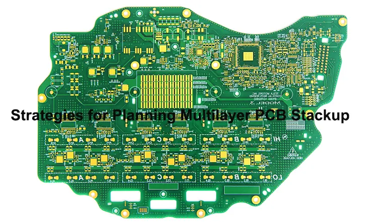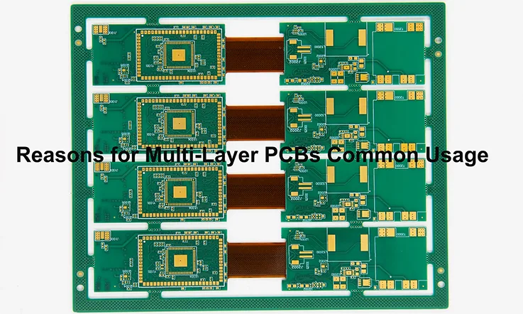
Multi-layer printed circuit boards (PCBs) are widely utilized in various industries for their ability to accommodate complex functionalities and compact designs. thought single-layer PCBs prove sufficient for devices necessitating simple, foundational features, the preference leans towards multilayer PCBs for more sophisticated undertakings. The demand for multi-layer PCBs has been on the rise as industries require smaller, more sophisticated devices.
Professional-grade electronics such as: computers, mobile devices, and medical equipment like cardiac monitors, typically engage multilayer PCBs due to these PCB boards versatility and capability to support complex circuitry. he fabrication process of multi-layer PCBs involves laminating multiple conductive layers together, with the number of layers varying based on the specific application requirements.. To illustrate, the PCBs integrated into mobile phones can incorporate upwards of 12 layers to accommodate the convoluted circuits required.
The advantages of multilayer PCB encompass an augmented circuitry capacity and an expansive suite of wiring options, rendering them the perfect candidate for challenging applications. Their versatility and ability to support complex designs make them a popular choice across various industries. Multi-layer printed circuit boards are widely utilized in various industries for their ability to accommodate complex functionalities and compact designs.
Multi-Layer PCB: Design Considerations
Designing a multi-layer PCB calls for numerous crucial considerations for guaranteeing peak performance and operability. Essential design considerations for multi-layer PCBs encompass:
Layer stackup:
Establishing the layer count, sequence, and thickness is paramount for optimizing signal integrity, power distribution and thermal management. Meticulous planning of the layer stackup is imperative to decrease signal disturbance and guarantee effective routing.
Signal integrity:
Preserving signal integrity is paramount in scenarios demanding high-speed operation.Proper impedance control, efficient signal routing, and minimal signal crosstalk are vital to avert signal deterioration and affirm dependable performance.
Power distribution:
Effective power distribution is essential for maintaining steady voltage levels and reducing voltage decreases over the PCB. The correct arrangement of power planes, vias, and decoupling capacitors is a necessary precondition for verifying uniform power distribution throughout the complete board.
Thermal management:
Effective administration of heat dissipation is critical to avert excessive heating and safeguard component reliability. Proper placement of thermal vias, heat sinks, and thermal pads can expedite efficient heat dispersion and sustain the optimal operational temperatures.
Component placement:
Strategic placement of components is crucial for minimizing signal interference, reducing signal path lengths, and optimizing the overall layout of the PCB. The placement of key components, connectors, and signal traces should be meticulously considered to ensure efficient routing and uphold signal integrity.
EMI/EMC considerations:
Multilayer PCBs are prone to electromagnetic interference (EMI) and electromagnetic compatibility (EMC) challenges. To mitigate EMI/EMC complications and secure compliance with regulatory benchmarks, the adoption of apt shielding measures, grounding techniques, and precise signal routing practices is crucial.
Design for manufacturability:
Creating a multilayer layer PCB that is easy to manufacture and assemble is crucial for cutting down production expenses and guaranteeing top notch PCBs. Improving factors like where componentsre positioned, trace widths and via placements is key, to promoting streamlined manufacturing procedures.
Benefits of Multi-Layer PCBs
Multi-layer PCBs present numerous advantages in contrast to single-layer or double-layer PCBs. The following are some prominent merits of employing multi-layer PCBs:
Compact Design: Multi-layer PCBs accommodate a more significant density of circuit elements and interconnections. By stacking multiple layers of copper traces and insulative layers, it’s viable to obtain a more condensed layout whilst housing a plethora of components. This is notably beneficial in intricate electronic apparatus where spatial is at a premium.
Reduced Size and Weight: The capacity to incorporate an abundance of components within a more confined space makes multi-layer PCBs instrumental in diminishing the comprehensive size and weight of electronic devices. Such benefit holds substantial importance in portable devices such as smartphones, tablets, and wearable tech, where the need for miniaturization is a prime concern.
Enhanced Signal Integrity: Multi-layer PCB ensure enhanced signal integrity and diminished electromagnetic interference (EMI). By isolating sensitive analog or digital signals from high-velocity or noisy signals on distinct layers, it’s possible to minimize cross-talk and interference. Consequently, leading to improved performance and reliability of the circuit.
Increased Design Flexibility: Multi-layer PCB provide more design flexibility relative to single-layer or double-layer boards. With multiple layers, designers can route traces in different directions and optimize signal paths, power distribution, and ground planes. Such strategic design improves the overall performance and functionality of the circuit.
Higher Circuit Complexity: Multi layer PCB enable the integration of complex circuitry. With the increase in the number of layers, the probabilities for interconnectivity escalate exponentially, facilitating the integration of more sophisticated features and functionalities. This is distinctly beneficial for high-performance application such as innovative microprocessors, memory modules, and fast-paced communication systems.
Improved Power Distribution: Multi-layer PCBs facilitate efficient power distribution throughout the circuit. Dedicated power and ground planes can be incorporated into the design, reducing impedance and voltage drops. This helps ensure stable voltage levels across the board, minimizing the risk of power-related issues and improving overall system reliability.
Ease of Testing and Troubleshooting: Multi-layer PCB simplify testing and troubleshooting processes. With multiple layers, it is easier to probe specific signals or access different parts of the circuit for testing or diagnosis.This results in significant savings in terms of time and exertion during the development and upkeep phases of electronic systems.
Why are Multi-Layer PCBs Commonly Used?
Multi layer PCB are frequently employed in electronic gadgets due to their multiple benefits compared to single-layer or double-layer PCB. Some of the factors for favoring multi-layer PCBs encompass:
Increased functionality: Multi-layer PCBs possess varied strata of conductive paths partitioned by insulating layers, providing an arena for intricate circuitries and amplified functionality within a minimal area. This is especially important in modern electronic devices that require high levels of integration and miniaturization.
Improved signal integrity: The various layers present in a multi-layer PCB grant superior signal integrity by diminishing electromagnetic disturbance and crosstalk amidst diverse components and paths. This is indispensable for high-speed and high-frequency uses where signal excellence is of paramount importance.
Better thermal management: Multi-layer PCBs facilitate effective dispersal of heat produced by electronic components, lessening the possibility of overheating and enhancing perpetual reliability and performance.
Higher density: Multi-layer PCBs can entertain a superior density of elements and paths, facilitating more condensed and effective layouts. This aspect is especially vital in gadgets that have stringent space restrictions.
Enhanced reliability: The multiple layers in a multi-layer PCB afford extra shielding from environmental elements like humidity, particulates, and oscillation, enhancing the total dependability and lifespan of the electronic gadget.
In entirety, the application of multi-layer PCBs empowers designers to construct more intricate, condensed, and trustworthy electronic devices that cater to the needs of contemporary technology.
Manufacturing Challenges and Solutions
The fabrication of multi-layer PCBs presents several challenges that must be tackled to guarantee the final product’s quality and dependability. Some usual fabrication challenges and their appropriate resolutions include:
Registration and alignment: Maintaining precise registration and alignment of multiple layers during the lamination process is crucial to avoid misalignment issues that can affect signal integrity. Using cutting-edge registration systems, laser drilling methodologies, and automated optical inspection (AOI) can assist in guaranteeing accurate alignment and registration.
Copper plating and etching: Achieving uniform copper plating and etching across multiple layers can be challenging, leading to issues such as uneven trace widths and signal degradation. Implementing controlled processes, including electroless copper deposition and precise etching techniques, can help achieve consistent copper thickness and trace quality.
Vias and interconnects: Creating vias and interconnects between layers in multi-layer PCBs requires precise drilling and plating processes. Utilizing advanced drilling technologies such as laser drilling and implementing controlled plating processes can ensure reliable vias and interconnects for signal transmission.
Thermal management: Efficient thermal management is critical in multi-layer PCBs to avoid excessive heat and guarantee component dependability. The inclusion of thermal vias, heat sinks, and thermal pads in the design can favor efficient heat dissipation and sustain ideal functioning temperatures.
Material selection: The selection of suitable materials for multi-layer PCBs is a crucial factor in guaranteeing performance and dependability. Electing high-grade laminate materials with the correct dielectric properties, thermal conductivity, and reliability can aid in addressing challenges like signal dissipation, thermal concerns, and material wear and tear.
Testing and inspection: Conducting thorough testing and inspection processes are essential to spot any production imperfections or problems in multi-layer PCBs. The deployment of automated examination apparatuses such as flying probe examiners and AOI systems, can facilitate early detection of defects in the manufacturing phase and safeguard the quality of the end product.
By aptly addressing these fabrication complications with suitable solutions, PCB manufacturers are capable of generating top-tier multi-layer PCBs that satisfy performance benchmarks, reliability norms, and customer anticipations.
Cost Considerations
Cost considerations hold considerable influence in the design and fabrication process of multilayer PCBs. There are several crucial elements that considerably affect the expense of multilayer PCBs, consisting of:
Number of layers:
The number of layers in a PCB directly impacts the manufacturing cost. With an augmentation in the number of layers, there is a subsequent rise in design intricacy, material requirements, and manufacturing process complexity, which cumulatively contribute to escalating production expenses.
Material selection:
Selecting for suitable materials for multilayer PCBs is imperative for their operational efficiency and stability, with potential cost implications. Superior-grade laminate materials possessing distinct attributes like thermal conductivity, dielectric constant, and reliability could come with a steeper cost than their standard counterparts.
Manufacturing processes:
The production procedures encompassed in creating multilayer PCBs, including lamination, drilling, plating, and etching, are part of the total investment. Complicated processes, advanced techniques, and intricate machinery necessitated for multilayer PCB manufacture have the potential to elevate the production expenses.
Component density and complexity:
The density and complexity of components on a multi-layer PCB can impact the cost of assembly and testing. Higher component density, fine pitch components, and complex designs require more precise assembly processes and testing procedures, leading to increased costs.
Quality and reliability requirements:
Meeting specific quality and reliability standards, like IPC standards or clientele stipulations, might necessitate further testing, inspection, and process control measures. These additional operations may contribute to the comprehensive expenditure of producing multilayer PCBs.
Design complexity:
The complexity of the PCB design, including the number of signal layers, routing requirements, and impedance control, can influence the cost of manufacturing. Complex designs that require advanced routing techniques, controlled impedance, and signal integrity considerations may incur higher production costs.
To manage costs effectively when designing and manufacturing multi-layer PCBs, it is essential to consider these factors and make informed decisions regarding materials, processes, and design complexity.
Contact JarnisTech for Multilayer PCB Manufacturing
In possessing extensive know-how in the blueprinting, manufacturing, and provision of multilayer PCBs, JarnisTech stands as a reliable partner. Should you find yourself necessitating services related to multilayer PCB production or assembly, we strongly encourage you to contact us today!
For direct communication, you’re welcome to dial 0086-0755-23034656 or forward an email to [email protected]. We eagerly await the opportunity to provide solutions for your multilayer PCB needs.
In conclusion
Multilayer PCBs furnish copious advantages, making them a sought-after option across a broad spectrum of electronic applications. Boasting greater design adaptability, superior signal integrity, advanced thermal management, heightened component density, and improved EMI/RFI shielding abilities, multilayer PCBs present a trustworthy and proficient resolution for the intricate electronic systems of the present day.
In summation, the benefits offered by multilayer PCBs render them as a flexible and cost-efficient choice for a plethora of industries, encompassing telecommunications, automotive, aerospace, and consumer electronics. Their ability to accommodate advanced designs, improve performance and amplify reliability makes them indispensable in modern electronic devices.
Our services
Multilayer PCB Manufacturing & Assembly

