In the production process of rigid-flex PCB circuit boards, meticulous orchestration of the stack up is indispensable to guarantee peak performance and trustworthiness. The stack up determines the sequence of layers, the materials incorporated, and the aggregate configuration of the board. Through strategical formulation of the stack up, engineers can cater to requirements such as signal integrity, thermal management, flexibility and manufacturability requirements. This article scrutinizes pivotal considerations and steps essential in devising the stack up for rigid-flex PCB circuit boards.
What is Rigid Flex PCB Stack up?
Rigid-flex PCB stack up refers to the arrangement of the layers in a printed circuit board that combines both flexible and rigid sections. It is predominantly utilized in electronic equipment demanding a convergence of both flexibility and rigidity are required.
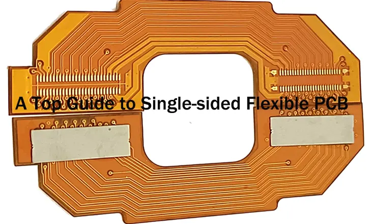
The stack up generally encompasses a commutation of stratums incorporating flexible constituents, polyimide for instance, and rigid constituents, like FR4. The flexible layers permit the board to exhibit bending or flexing properties, while the rigid layers confer stableness and a supportive infrastructure for components and connectors.
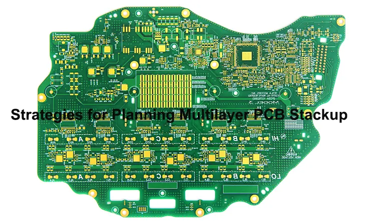
The design of the stack up can exhibit variations hinging on the precise stipulations of the utilized applications. It may encompass numerous flex layers, rigid layers, along with buried vias to furnish electrical linkage between the divergent layers.
The conceptualization of the stack-up design also contemplates the electrical efficiency of the board, such as impedance control and signal integrity. Ground and power planes are often included to provide shielding and reduce electromagnetic interference.
In essence, the rigid-flex PCB stack-up exemplifies a specialized design allowing the amalgamation of flexibility and rigidity in electronic apparatuses, thereby facilitating more compact and durable designs.
Key Features of Rigid-Flex PCB Stack-up Configuration
1. Reduced solder joints and connectors: Rigid-flex stack-up eradicates the necessity for supplementary connectors and solder junctions, diminishing the hazard of soldering discrepancies and possible circuit malfunctions. This streamlines the assembly procedure and amplifies dependability.
2. Thin board thickness: Rigid-flex technology allows the effective condensation of the board thickness, customarily varying from 0.2mm to 0.4mm. This slim profile supplements the collective durability and flexibility of the PCB.
3. High thermal strength: Rigid-flex PCB excel in heat dissipation, providing superior thermal performance compared to conventional rigid boards. his characteristic ensures proficient alleviation of heat, augmenting the trustworthiness of the electronic apparatus.
4. High aspect ratio: Rigid-flex stack-up allows for a high aspect ratio, where the width of the tracks is greater than their height. This particularity offers more space between components, aiding in better signal transmission. It further streamlines the course routing of wires and ancillary components.
5. Solder masking: Solder masking is a protective layer that defines the component positions on the PCB. It safeguards against damage triggered by abrasion and offers a shield from electrostatic discharge. By applying an ink-receptive coating to the board, the solder mask to ensures the integrity of components.
These vital attributes of the rigid-flex PCB stack-up bolster its aptness for an array of applications, notably those demanding flexibility, durability, and high-caliber performance traits. The stack-up design can be tailored to meet specific requirements, ensuring optimal functionality and reliability in electronic devices.
The Significance of Rigid-Flex PCB Stack-up Design
The design of a rigid-flexible PCB stack-up is notably vital in assuring the serviceability, dependability, and fabricability of the board. Here are some principal reasons depicting the cruciality of the stack-up design:
1.Flexibility and rigidity integration:
Rigid-flexible PCB amalgamate the beneficial aspects of both pliable and rigid materials. The stack-up design dictates the arrangement and layering of these materials, allowing for seamless integration of flexible and rigid sections. This integration is essential in applications where the PCB needs to flex, revolve, or adapt into compact spaces while sustaining stability and support for components.
2.Electrical performance:
The stack-up design directly affects the electrical functioning of the PCB. It determines the positioning of signal, power, and ground strata, and also the pathing of traces and vias. Proper stack up design helps achieve controlled impedance, minimize signal loss, and ensure proper power distribution, thus enhancing the overall electrical performance of the board.
3.Signal integrity and EMI/EMC considerations:
Rigid-flexible PCB stack-up design holds a critical position in upholding signal veracity and diminishing electromagnetic disruption (EMI) and electromagnetic resonance (EMC) difficulties. By carefully selecting and arranging the layers, proper shielding can be achieved to minimize noise and interference between different circuit sections. This is especially important in high-speed and sensitive applications.
4.Thermal management:
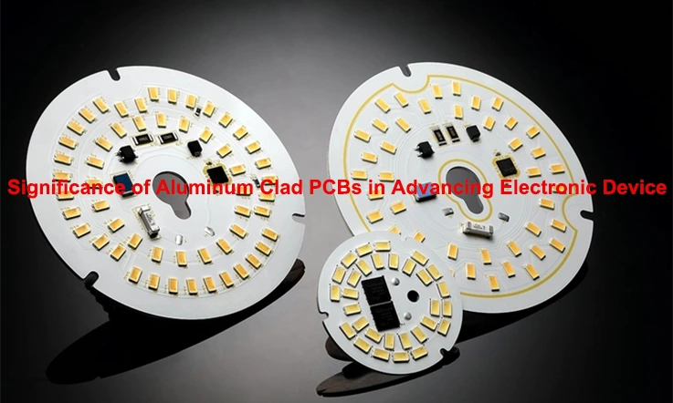
Effective heat removal is vital for the trustworthy functioning of electronic equipment. The stack-up arrangement should regard the location of thermal vias, power planes, and heat dissipaters for assuring effective thermal management. Through ideal stack-up optimization, heat can be competently escorted away from essential elements, averting overheating and potential decline in performance.
5.Manufacturing and assembly considerations:
The stack-up design should also consider the manufacturing and assembly processes. It ought to weigh the competencies of PCB fabrication and assembly equipment, including the maximum count of layers, minimum trace breadth/separation, and alignment prerequisites. A well-thought-out stack up can streamline the production routine, diminish fabrication expenses, and enhance the aggregate output and reliability of the PCB.
Therefore, the stack up design of a rigid-flex PCB is significant as it determines the integration of flexibility and rigidity, influences the electrical performance, ensures signal integrity and EMI/EMC compliance, enables effective thermal management, and considers manufacturing and assembly considerations. A meticulously designed stack-up is pivotal for the realization of a functional, dependable, and producible rigid-flex PCB.
Purpose of Rigid Flex PCB Stack up
The fabrication process of flex-rigid boards affords heightened adaptability in comparison to conventional printed circuit boards, positioning it as a favored option for the inception of innovative products. These boards provide faster production times and allow for optimized space utilization, which is crucial in product development.
The integration of flexible components into circuit boards reduces the need for additional connectors, thereby augmenting assembly efficiency and diminishing overall mass. This streamlined design approach, unique to rigid-flex stack up, contributes to improved performance and functionality.
Moreover, rigid-flex printed circuit boards tackle the frequently faced space and weight restrictions inherent in standard PCBs. The optimal design and assembly of rigid-flex boards proficiently counter these challenges, fostering the creation of condensed and light electronic apparatuses.
Therefore, the versatility of flex-rigid board fabrication, coupled with its ability to optimize space utilization and reduce weight, posits it as an exemplary solution to transcend traditional PCB confines in the progression of avant-garde products.
Applications of Rigid-Flex PCB Stack-up in Various Industries
Rigid-flex PCB stack up offers the unique advantage of being easily moldable into desired shapes, making it highly versatile for a wide range of applications. The sophisticated technology incorporated into the rigid-flex stack-up underpins faster performance speeds, marking it as a fitting choice for diverse industry applications. Several substantial uses of rigid-flex PCB encompass:
●Consumer Appliances
●Telecommunications
●Medical Equipment
●Automotive
●Industrial
●Aerospace
●Military
The Importance of Rigid-Flex PCB Stack-up Design
Rigid-flex PCB stack-up design plays a crucial role in ensuring the functionality, reliability, and durability of electronic devices.
1.Space Optimization: The design of a rigid-flex PCB stack-up affords the merging of both rigid and flexible segments into one board, resulting in notable space conservation. This becomes particularly advantageous in scenarios where dimension and weight limitations are vital, such as mobile devices and aerospace systems. With effective usage of the allotted space, the rigid-flex stack-up design facilitates the creation of sleek and lightweight electronic devices.
2. Improved Signal Integrity: The design of a rigid-flex PCB stack-up assists in diminishing signal degradation and disturbance. Precise design of the stack-up allows for the routing of signal traces in the most advantageous manner, subsequently minimizing the length and impedance discrepancy. This results in superior signal integrity, decreased signal loss, and elevated overall performance of the electronic system.
3. Increased Dependability: Merging rigid and flexible sections onto one board results in improved reliability as opposed to employing separate rigid and flexible PCBs. By eliminating connectors and interlinking cables, the likelihood of mechanical breakdowns is reduced, thereby enhancing the system’s overall robustness. Furthermore, Rigid-flex stack up design also provides better resistance to mechanical stress, vibration, and thermal cycling, making it suitable for applications in harsh environments.
4. Streamlined Assembly: The incorporation of a rigid-flex PCB stack-up design facilitates a simplified assembly procedure by diminishing the requirement for multiple interconnections and connectors. This leads to a streamlined manufacturing process, lower assembly costs, and improved overall production efficiency. The elimination of interconnecting cables and connectors also minimizes the potential for assembly mistakes, boosting the dependability and quality of the end product.
5. Design Flexibility: In contrast to traditional rigid PCB, the rigid-flex PCB stack up design grants superior design flexibility. It allows for the creation of complex shapes and three-dimensional configurations, enabling the development of innovative and unique electronic devices. The pliability of the stack up design allows the PCB to adapt to the shape and contours of the device, enhancing further to the design possibilities.
Materials Used in Rigid-Flex PCB Stack up Construction
1. Copper Foil: Copper is a commonly used conductive trace layer in rigid-flex boards. It is used to form traces that connect power and ground planes or run within the circuit layers. Copper foil can be selected in different thicknesses, allowing for flexibility in routing smaller layers and minimizing waste.
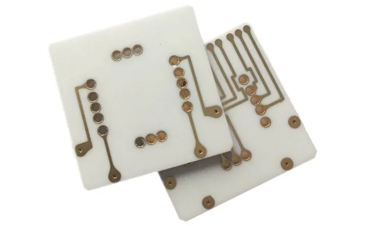
2. FR4: FR4 is a widely used material in PCB assembly that provides mechanical strength. It comprises a fiberglass cloth suffused with a flame-resistant epoxy resin binder, rendering it non-conductive. This component, FR4, is deployed in rigid-flex boards to furnish rigidity and buttress the entire architecture.
3. Prepreg: Prepreg is an insulating material used in rigid-flex PCB. It acts as a dielectric layer between two layers, typically a copper foil and a core. Prepreg serves as a binding material, connecting two cores or a core and copper foil, and providing electrical insulation.
4. Adhesive: Rigid-flex boards may necessitate the employment of adhesive to unite disparate circuit components. Depending on the unique requisites of the circuit, two types of PCB adhesives can be deployed. RTV (Room Temperature Vulcanizing) super glue, which is a non-acidic adhesive that undergoes curing at room temperature, is deemed fitting for applications where a leisurely curing process is preferred. On the other hand, Cyanoacrylate glue, also known colloquially as instant glue, furnishes rapid bonding when swift adherence is mandated.
By Leveraging these flexible board substrates, rigid-flex PCBs secure the indispensable amalgamation of flexibility and rigidity, fundamental in addressing the design and functional necessities of numerous electronic devices. The thoughtful choice and use of these substrates play a crucial role in enhancing the overall efficiency, reliability, and durability of the rigid-flex boards.
How Many Types for Rigid Flex PCB Stack-up?
There are many common stack up configurations, for rigid flex PCB that can be used depending on the specific design needs. The commonly used types include:
Sided Rigid Flex Stack-up: This setup includes one rigid layer and one flexible layer, suitable for simple applications that only require a single flexible section.
Double Sided Rigid Flex Stack-up: In this design two rigid layers are combined with one or more flexible layers allowing for more intricate designs with multiple flexible sections and increased routing possibilities.
Multi layer Rigid Flex Stack-up: This stack up comprises rigid and flexible layers offering maximum design flexibility, for integrating complex circuits, high density components and advanced functions.
Every kind of stack-up layout presents exclusive benefits, and the selection is determined by aspects such as the intricacy of the design, spatial limitations, requirements for signal integrity, and manufacturing contemplations. The decision regarding the stack-up layout is integral to guaranteeing superior performance, trustworthiness, and ease of manufacturing of the rigid-flex PCB.
Conclusion
Properly planning the stack-up for rigid-flex PCB circuit boards is vital for successful design implementation. Considering determinants like signal integrity, thermal management, flexibility and manufacturability, designers can create stack up configurations that meet the specific requirements of the application. In additional, a strategically arranged stack-up underpins optimum performance, dependability, and manufacturability, at the same time, it contributing to the overall success of the rigid-flex PCB circuit board design.


