
Rigid-flex PCB offer a remarkable solution for seamlessly integrating multiple rigid PCB through flexible circuits within a single assembly. This innovative approach, combining rigid and flexible materials on a single board, enables the realization of three-dimensional packaging and enhanced component density within electronic devices.
A 6-layer rigid-flex PCB, as the name suggests, involves a stack-up configuration comprising six conductive copper layers. This article aims to provide a comprehensive overview of the technology behind 6-layer rigid-flex PCB, encompassing various essential aspects.
What is 6-Layer Rigid-Flex PCB Circuit Board?
A 6-layer rigid-flex PCB circuit board is a unique types of printed circuit board, employing both rigid and flexible substrates to formulate a multi layer construction. It embodies six conductive copper strata, facilitating electrical connections and establishing points for component mounting.
The rigid sections of the PCB are typically made of traditional FR-4 or high-frequency materials, offering stability and mechanical support for components. These sections are rigid and cannot be bent or flexed.
On the other hand, the supple segments of the PCB are manifested using flexible materials like polyimide. Such flexible substrates enable the PCB to exhibit bending, folding or flexing characteristics as required, enabling the amalgamation of the rigid segments into three-dimensional assemblies. The flexible sections provide connectivity between different rigid layers and facilitate movement within electronic devices.
The layers of the 6-layer rigid-flex PCB are stacked together, with the rigid layers and flexible layers interleaved. Vias and interconnections are created through drilling and copper plating processes, ensuring electrical continuity between the layers. Copper traces are selectively etched to form circuit patterns, and the layers are laminated together under heat and pressure.
The combination of rigid and flexible sections in 6 layer rigid-flex PCB allows for compact and intricate designs that can overcome the limitations of traditional rigid PCB. It enables efficient utilization of space within electronic devices, enhances reliability by reducing the need for connectors and cables, and improves signal integrity by minimizing signal loss and electromagnetic interference.
Construction and Materials of 6 Layer Rigid-flex PCB
The fabrication of a 6-layer rigid-flex PCB necessitates the implementation of particular materials that conjugate rigid and flexible substrate Here is a synthesis of the fabrication and materials entailed in a standard 6-layer rigid-flex PCB:
Rigid Layers:
Core Material: Conventionally, the rigid strata of the PCB are fabricated from FR-4 (Fire Resistant-4) or analogous high-frequency laminates. Renowned for superior electrical insulating attributes and mechanical steadiness, FR-4 is an epoxy-based material extensively employed.
Copper Foil: A thin layer of copper foil is bonded to the surfaces of the rigid layers. Serving as the conductive substance for the formulation of circuit traces and establishment of electrical linkages, the copper foil is indispensable.
Flexible Layers:
Polyimide (PI):The flexible layers of the PCB usually consist of polyimide film, known for its durability and flexibility to endure bending and flexing while maintaining its properties.
Adhesive: A thermally resilient adhesive is deployed for affixing the copper foil to the polyimide strata. The adhesive stratum is instrumental in securing the mechanical integrity of the flexible sections.
Adhesive Layers:
Prepreg: Often referred to as pre-impregnated resin, prepreg is a compound substance comprising a resin matrix pervaded with glass filaments. It is used as an adhesive layer to bond the rigid and flexible layers together during the lamination process.
Bonding Sheets: Bonding sheets are often employed to provide additional adhesion and stability between the layers. Typically composed of epoxy-base materials, these sheets possess the capability to endure elevated temperatures and assure dependable bonding.
Copper Interconnections:
Vias: Vias are small holes drilled through the layers of the PCB, connecting different conductor layers. These vias are plated with copper to establish electrical connections between the layers.
Plated Through-Holes (PTH): Plated through-holes are larger vias used to connect components and provide interconnections between different layers of the PCB.
These construction materials and layers are carefully selected and combined to create a 6-layer rigid-flex PCB that offers both mechanical stability and flexible functionality. The layers are stacked together, and they tread through drilling, coating, plating etching, and laminating phases during the fabrication procedure to shape the eventual rigid-flex PCB structure.
Common of 6 Layer Rigid-flex PCB Stack-up
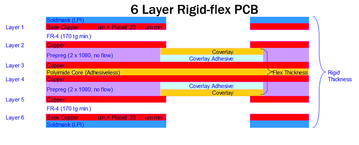
A common six-layer rigid-flex PCB stack-up typically includes alternating layers of rigid and flexible materials. Here’s an example of a common six-layer rigid-flex PCB stack-up:
1 Layer: The primary foundational layer of the stack-up typically comprises a substrate material like FR4. This layer potentially houses signal traces, as well as power and ground planes.
2 Layer: This layer, molded from a flexible material akin to polyimide (PI), is engineered to accommodate bending and flexing movements. It may also incorporate additional signal traces or power planes.
3 Layer: As another rigid layer resembling Layer 1, it serves to provide essential structural support and protection for the underlying flex layers. Possibilities include the presence of signal traces, power planes, and ground planes.
4 Layer: In likeness to Layer 2, this layer is added to enhance flexibility. It may host signal traces or power planes.
5 Layer: Possessing comparable rigidity to Layers 1 and 3, the fifth layer further strengthens the stack-up and could harbor signal traces, power planes, and ground planes.
6 Layer: Finally at the top of the stack up sits the layer. A rigid one similar to layers 1 and 3. Offering ultimate structural support, with possible signal traces, power planes and ground planes.
It’s important to note that the specific materials, thicknesses, and order of layers in a rigid-flex PCB stack-up can vary depending on the application, design requirements and manufacturer’s capabilities. Intricate designs might encompass additional layers of rigid and flexible materials. Collaborating intimately with a PCB fabricator or design engineer to determine the best stack-up for your unique project is advocated.
6 Layer Rigid Flex PCB Fabrication Process
The fabrication process for a 6-layer rigid-flex PCB involves several key steps to create the layered structure and interconnections between the rigid and flexible sections. Here is a general overview of the fabrication process:
Layer Stacking:
Preparing Rigid and Flexible Layers: The rigid and flexible layers, made of FR-4 and polyimide respectively, are prepared with copper foil attached to their surfaces.
Aligning and Stacking Layers: The layers are carefully aligned, ensuring that the copper traces and vias align properly for interconnections between layers.
Drilling and Plating:
Drilling: Small holes, known as vias, are drilled through the stacked layers at specific locations to establish electrical connections between the layers.
Desmear and Plating: The drilled vias are treated to remove any debris or smear caused by the drilling process. They are then plated with a conductive material, usually copper, to create electrical pathways.
Etching and Lamination:
Etching: Copper traces and circuit patterns are formed by selectively etching away excess copper from the surface using a chemical process. This creates the desired circuitry on each layer.
Lamination: The etched layers, along with prepreg layers, are stacked and pressed together under heat and pressure. The heat activates the adhesive properties of the prepreg, bonding the layers together to form a solid structure.
Surface Finishing:
Solder Mask Application: A solder mask layer is applied to the surface of the PCB, covering the copper traces and leaving only the desired areas exposed for soldering components.
Copper Plating and Outer Layer Etching: Outer layers are copper-plated to provide a protective and conductive surface. Excess copper is then etched away to reveal the desired circuitry and patterns.
Surface Finish: A surface finish is applied to protect the exposed copper and provide a solderable surface. Common surface finishes include HASL (Hot Air Solder Leveling), ENIG (Electroless Nickel Immersion Gold), and immersion silver.
Amid the manufacturing procedure, quality control measures, including inspections and tests, are undertaken to validate the integrity of the PCB and conformance to design prerequisites.
It is important to note that the specific details of the fabrication process may vary depending on factors such as the PCB manufacturer’s capabilities, design requirements, and industry standards.
6 Layer Rigid-flex PCB Board Design Guidelines
Designing a six-layer rigid-flex PCB demands meticulous scrutiny of an array of aspects to assure prime performance, dependability, and fabricatability. Here are several vital design directives to remember for six-layer rigid-flex PCB boards:
Bend Radius Considerations:
Determine Minimum Bend Radius: Identify the minimum allowable bend radius for the flexible sections of the PCB. This ensures that the flexible material can withstand repeated bending without damage.
Avoid Sharp Corners: Minimize the use of sharp corners in the flexible sections as they can weaken the material and lead to failure over time.
Provide Sufficient Clearance: Ensure that there is adequate clearance between components and the bend areas to avoid interference during bending.
Trace Routing Techniques:
Differential Pair Routing: If your design involves high-speed signals, consider routing differential pairs to maintain signal integrity and minimize crosstalk.
Controlled Impedance Routing: For impedance-controlled signals, use appropriate trace widths and spacing to achieve the desired impedance values and ensure signal integrity.
Avoid Right-Angle Traces: Minimize the use of right-angle traces as they can cause signal reflection and impedance mismatch. Instead, use gradual curves or mitered corners.
Component Placement Strategies:
Flexible and Rigid Placement: Consider the electrical factors when deciding where to place different components. Components, in areas should be able to withstand bending and flexing. Components located in flexible regions ought to be resilient to bending and flexing.
Keep Components Away from Bend Areas: Place sensitive or delicate components away from the bend areas to avoid mechanical stress or damage during flexing.
Thermal Management: Assess the thermal properties of components, and ascertain that heat dispersal is adequately administered, particularly in zones where rigid and flexible sections maintain close proximity.
Signal Integrity and EMI Considerations:
Ground Plane Placement: Utilize dedicated ground planes to provide proper grounding and minimize noise.
Signal Layer Arrangement: Arrange signal layers in a way that minimizes cross talk and interference between adjacent layers, especially in the flexible areas.
Shielding and EMI Protection: Incorporate shielding techniques and ground planes to protect sensitive signals from electromagnetic interference (EMI).
Testability and Accessibility:
Test Points: Include appropriate test points for ease of testing and troubleshooting during production and maintenance.
Connector Placement: Ensure that connectors or test points are accessible and can be easily connected or probed for testing purposes.
Design for Manufacturability:
Design Rule Check (DRC): Execute a design rule validation to affirm that the design meets the manufacturing capacities and tolerances outlined by the PCB producer.
Layer Stacking Considerations: Plan the layer stackup carefully, considering the thickness and arrangement of the rigid and flexible layers to achieve desired flexibility and mechanical stability.
Keep Traces Symmetrical: Maintain symmetrical trace routing in flexible areas to distribute stress evenly during bending.
By following these design guidelines, you can optimize the functionality, reliability, and manufacturability of your 6-layer rigid-flex PCB design. However, it’s important to consult with your PCB manufacturer and consider specific design rules and guidelines provided by them for best results.
Assembly Considerations for 6 Layer Rigid-flex PCB
Flex-to-Rigid Connection: The assembly process requires specialized techniques to establish reliable connections between the flexible and rigid sections.
Component Compatibility: Components chosen for rigid-flex PCB assemblies should be suitable for the bending and flexing movements of the board.
Testing and Inspection: Thorough testing and inspection processes are indispensable to guarantee the dependability and functionality prowess of the assembled PCB.
What Factors Cost Impact on 6 Layer Rigid Flex?
The expenditure linked to a 6-layer rigid-flex PCB can be swayed by multiple determinants. Here, we provide key factors that can have a bearing on the cost.
Material Selection: The selection of materials for both rigid and flexible layers can have a substantial implication on the expenditure. FR-4, known for its common usage and cost-efficiency, is typically employed for the rigid sections, whilst polyimide, with a tendency to be pricier, is frequently utilized for the flexible segments. Higher-grade materials or specialized laminates can also increase the cost.
Layer Quantity: The total count of layers embodied in the PCB has a palpable effect on the costing. An upward surge in the number of layers corresponds to an increase in the intricacies of the production process and the quantity of material requisitioned, thereby, driving up the cost.
PCB Size and Complexity: Larger PCB generally require more material and longer manufacturing times, resulting in higher costs. Additionally, complex designs with intricate routing, multiple components, and fine pitch components can increase the manufacturing complexity and, consequently, the cost.
Manufacturing Processes: Certain manufacturing processes, such as drilling, plating, lamination, and specialized techniques for rigid-flex PCB, can add to the overall cost. For example, the drilling and plating of vias in multiple layers can increase costs compared to simpler PCB designs.
Design Specifications: Specific design requirements, such as controlled impedance, high-speed signaling, and tight tolerances, can impact the cost. These requirements may necessitate additional manufacturing steps, specialized materials, or stricter quality control measures, which can add to the overall cost.
Quantity and Lead Time: The quantity of PCB ordered and the desired lead time can influence the cost. Ordering a larger quantity can often result in volume discounts, while shorter lead times may incur additional charges for expedited manufacturing.
Manufacturer and Location: The choice of PCB manufacturer and their location can affect the cost. Different manufacturers have varying pricing structures, capabilities, and overhead costs that can impact the overall cost of the 6-layer rigid-flex PCB.
Rigid-flex PCB generally involve more complex manufacturing processes and specialized materials, which can impact the overall cost compared to traditional rigid PCB.
However, considering the benefits and increased functionality offered by rigid-flex technology, the cost is often justified in applications where space constraints, reliability, and performance are critical factors.
Benefits and Applications of 6 layer Rigid-flex Circuit Board
Enhanced Design Flexibility: Rigid-flex PCB enable intricate and compact designs, overcoming the limitations imposed by traditional rigid PCB.
Increased Reliability: The elimination of connectors and cables reduces the risk of failure due to mechanical stress or vibration.
Space Savings: The ability to fold or bend the flexible sections allows for efficient space utilization within electronic devices.
Improved Signal Integrity: Rigid-flex technology minimizes signal loss and electromagnetic interference, enhancing overall performance.
Diverse Applications: 6-layer rigid-flex PCB find applications in aerospace, medical devices, consumer electronics, and other industries demanding compact and reliable electronic assemblies.
Why Choose Us?
One of the Most Exceptional Rigid-flex PCB Manufacturers
JarnisTech has earned a strong reputation as a trusted and reliable supplier of rigid-flex circuit boards, satisfying the diverse manufacturing requirements of our valued customers. Our unwavering dedication to advanced rigid-flex PCB technology sets us apart in the industry.
With a team of highly skilled professionals specializing in rigid-flex circuits, we possess the expertise to comprehend your design swiftly, eliminating the need for repetitive explanations. This streamlined approach saves you valuable time, particularly during cross-timezone conversations. As our client, you can count on us to provide comprehensive Design for Manufacturability (DFM) support at the early stages of your project, ensuring smooth communication throughout, and delivering your order punctually.
Our most esteemed service is the provision of quick-turn rigid-flex PCB. Whether you require a single-layer rigid-flex circuit, a double-sided rigid-flex circuit, or a multi layer rigid-flex board featuring blind or buried vias, we guarantee superior quality and timely production. Our manufacturing capabilities extend to 36-layer rigid-flex PCB, enabling us to fulfill projects of varying complexity.
Should your project be time-critical, demanding fast prototyping to authenticate a novel concept, our expedited service is custom-made to satisfy your requirements. We pledge commitment to the prompt delivery of your “first-build” prototypes, affordably priced, facilitating rapid advancement with your product evolution.
For inquiries regarding the cost of rigid-flex PCBs, we encourage you to contact us without delay at [email protected]. By reaching out to us, you will engage with one of the foremost rigid-flex PCB manufacturers in China, ensuring exceptional service and superior product quality.
In Summary
6-layer rigid-flex PCB technology offers unique advantages, allowing for compact, reliable, and multifunctional electronic assemblies. By understanding the benefits, construction, fabrication process, design guidelines, assembly considerations, and cost impact, PCB manufacturers can harness the potential of this advanced technology to meet the evolving demands of various industries.


