
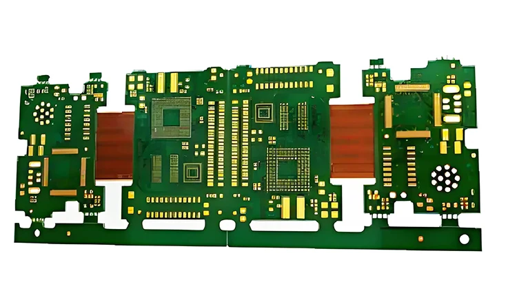
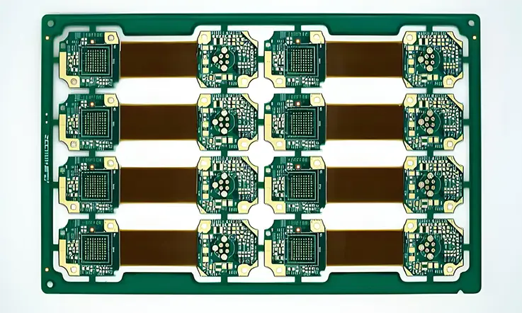
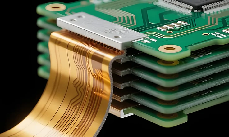
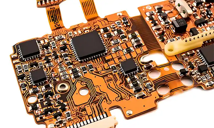
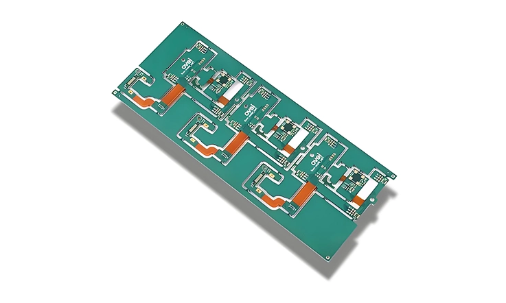
In the intricate world of advanced electronics, 12-layer rigid-flex circuits are a marvel of integrated design. They are not simply boards, but dynamic electromechanical structures that weave the stability of rigid platforms with the three-dimensional freedom of flexible substrates. This singular, unified construction dissolves the boundaries between board and cable, forging a path for devices that are more compact, more resilient, and more capable than ever before. This guide offers a journey through their creation, from architectural conception to final, functional reality.
The Architectural Blueprint: 12-Layer Stack-Up and Material Science
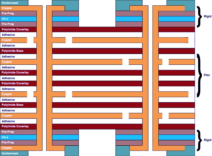
Every great structure begins with a blueprint. For a 12-layer rigid-flex board, that blueprint is the stack-up, a meticulously planned architecture of materials. This is where physics and foresight converge, defining the board’s character, its strength, and its ability to perform under pressure. The selection of each material is a deliberate choice, a commitment to performance and long-term reliability.
The Discipline of Symmetrical Design
Imagine a freshly laminated board cooling from over 180°C. If its layers of copper and dielectric are not perfectly balanced around its center, a microscopic tug-of-war begins within its structure. This internal conflict, born of mismatched thermal expansion, manifests as warpage. A symmetrical stack-up is the discipline that prevents this, creating an inherently stable platform that remains flat and true through the rigors of assembly and its operational life.
●Structural Equilibrium: By mirroring the layer sequence, the mechanical forces of expansion and contraction are neutralized. This is profoundly important when bonding dissimilar materials like FR-4 and polyimide, ensuring stress does not concentrate at their interface.
●Manufacturability: A stable, flat board moves through automated assembly lines with grace and precision. Warpage, by contrast, can disrupt everything from solder paste application to optical inspection, compromising quality and yield.
●Long-Term Endurance: Over thousands of thermal cycles in the field, a balanced board is less prone to stress-induced failures, such as solder joint fatigue or via cracking, ensuring the product’s longevity.
The Science of Material Selection
The choice of materials infuses the board with its fundamental properties. This is a careful balancing act, weighing the resilience needed for flexing against the stability required for component mounting, all while considering the subtle demands of high-speed electrical signals.
The Flexible Heart (Polyimide):
The soul of the flex circuit is its polyimide (PI) core. For high-performance applications, adhesiveless PI systems are specified. Here, copper is deposited directly onto the film, eliminating the traditional acrylic adhesive layer. This results in a thinner, more flexible circuit that can withstand higher temperatures and more bend cycles without the risk of adhesive delamination.
The Rigid Skeleton (High-Tg FR-4):
The rigid sections provide a solid foundation. To survive the intense heat of modern lead-free soldering processes, a high-Tg (glass transition temperature) FR-4 is specified. Materials with a Tg above 170°C maintain their structural integrity, preventing the delamination that can plague lesser materials.
The Conductive Pathways (Copper Foil):
The type of copper foil chosen speaks to the board’s intended life. For static, bend-to-install applications, standard Electro-Deposited (ED) copper suffices. For dynamic applications involving continuous movement, Rolled-Annealed (RA) copper is required. Its elongated grain structure gives it a superior ductility, allowing it to endure millions of flex cycles without fracturing.
The Protective Skin (Coverlay & Stiffeners):
A polyimide coverlay acts as a flexible solder mask, insulating and protecting the delicate traces on the flex sections. In areas where components or connectors need a firm footing, stiffeners—small, precisely placed pieces of FR-4 or polyimide—are bonded to the flex, providing localized rigidity without compromising the overall flexibility of the design.
Material About 12 Layer Rigid-flex PCB Stack-up:
Deciding on the appropriate materials for 12 layer rigid flex PCB stack-up is influenced by a multitude of aspects. These often include the requirements of the application, the desired mechanical and electrical performance, and the available manufacturing competencies. Following are the materials traditionally adopted for each layer in 12 layer rigid flex PCB stack-up:
1.Outer layers (rigid sections):
Copper foil: Typically used for signal traces and power distribution.
FR-4 (Fire-Resistant 4): A widely used epoxy-based laminate material that provides good electrical insulation and mechanical strength.
2.Inner layers (rigid sections):
Copper foil: Used for additional signal routing, power planes, or ground planes.
Prepreg: Layers of fiberglass cloth impregnated with epoxy resin, used for bonding the copper layers together.
3.Flex layers:
Polyimide : A highly flexible and heat-resistant material that serves as the base substrate for the flexible regions. It offers excellent mechanical properties and can withstand repeated flexing without degradation.
Adhesive: Used to bond the polyimide layers together in the flex region.
4.Vias:
Copper-plated vias: Used to provide electrical connections between different layers, including rigid and flex regions.
It’s important to note that the specific material choices and layer configurations within a 12-layer rigid-flex PCB stack-up can vary based on design requirements, manufacturing capabilities, and the choice of the PCB manufacturer.
Mastering Signal Integrity in High-Speed Rigid-Flex Designs
With the physical blueprint established, attention turns to the invisible lifeblood the board will carry: electrical signals. On a 12-layer board, these signals travel through a dense and complex environment. Preserving their purity—their signal integrity—is a fundamental challenge. It requires treating the copper traces not as simple wires, but as finely tuned transmission lines.
Controlled Impedance: The Rule of the Road
A high-speed signal benefits from a well-defined routing structure. Controlled impedance enables the signal to travel along its intended path, allowing energy to transfer efficiently from transmitter to receiver while minimizing unwanted echoes or disruptions.
The Transmission Line Concept:
Every trace on a PCB has a characteristic impedance, determined by its physical dimensions and the dielectric material around it. A 12-layer structure provides a rich environment for creating these transmission lines, either as microstrips on the surface or shielded striplines within the inner layers.
Differential Pairs:
For the fastest data rates, signals are often sent as differential pairs—two traces working in tandem. This technique offers excellent noise rejection and is the standard for interfaces like USB and Ethernet. The differential impedance of this pair is a parameter that must be precisely maintained.
The Rigid-to-Flex Transition:
One aspect that requires careful handling is the interface where the circuit transitions from rigid to flexible material. Because FR-4 and polyimide differ in their dielectric characteristics, keeping the trace width unchanged would lead to a shift in impedance. Advanced layouts gradually adjust the trace width across this zone, allowing the signal to travel through without unexpected electrical behavior.
Taming Crosstalk and Emissions
In the dense city of a 12-layer board, traces run in close proximity, and their electromagnetic fields can interfere with one another. This “crosstalk” can corrupt data and is a primary signal integrity concern.
Strategic Spacing and Routing:
The most effective way to reduce crosstalk is to provide adequate spacing between traces. Routing adjacent signal layers orthogonally (one layer horizontal, the next vertical) is another powerful technique that minimizes the length over which traces can couple.
The Role of Reference Planes:
Solid ground and power planes are exceptional shields. They not only provide a return path for signals but also isolate layers from one another. A signal’s return current will always seek the path of least impedance, and a continuous, unbroken reference plane provides a direct, low-noise route.
Specialized Shielding:
For the most sensitive applications, or in flexible areas where solid planes are not feasible, specialized EMI shielding films can be applied. These flexible, conductive films act like a form of micro-coaxial shielding, containing the board’s emissions and protecting it from external noise.
Advanced Thermal Management Strategies for Dense PCB Layouts
As electronic components become more powerful and compact, managing the heat they generate is a formidable engineering challenge. A 12-layer board, with its dense circuitry and multiple insulating layers, can trap heat if not designed with a deliberate thermal strategy. Effective thermal management is not an afterthought; it is a parallel design discipline that ensures the board operates within safe temperature limits, promoting reliability and preventing premature failure.
Conductive Heat Dissipation Pathways
The primary goal of thermal management is to create low-resistance pathways for heat to move from its source (like a processor or power IC) to a place where it can be safely dissipated.
●Thermal Vias: This is the most common technique. An array of vias is placed directly under a heat-generating component, connecting its thermal pad to large copper planes on other layers. These vias, often filled with thermally conductive epoxy, act like pillars, wicking heat away from the component and spreading it laterally through the copper planes.
●Copper Planes: Large, solid copper planes on the inner and outer layers of the board are excellent heat spreaders. By connecting thermal vias to these planes, the concentrated heat from a small component can be distributed over a much larger area, lowering the peak temperature.
●Heavy Copper Traces: For high-current applications, using heavy copper (2 oz. or more) for power traces not only reduces electrical resistance but also provides a substantial pathway for heat to conduct away from power components like MOSFETs and regulators.
Advanced and External Cooling Solutions
For the most demanding applications, passive conduction through the board alone is not enough. More advanced techniques are required to actively remove heat from the system.
●Embedded Coins and Slugs: In this advanced technique, a solid copper or aluminum “coin” is embedded into a cutout in the PCB directly beneath a major heat source. This provides a direct, highly efficient thermal path from the component to a heat sink on the other side of the board, bypassing the higher thermal resistance of the board’s dielectric layers.
●Heat Sinks: For components generating significant wattage, an external heat sink is often necessary. The PCB must be designed to accommodate this, with clear mounting holes and a flat, thermally prepared surface to ensure good contact between the component, the board, and the heat sink.
●Thermal Interface Materials (TIMs): No surface is perfectly flat. TIMs, such as thermal grease, pads, or phase-change materials, are used to fill the microscopic air gaps between a component and its heat sink. This displaces the insulating air and dramatically improves the efficiency of heat transfer.
The Art of Miniaturization: High-Density Interconnect (HDI) in Practice
High-Density Interconnect (HDI) technology is what allows a 12-layer design to achieve its full potential for miniaturization. It is a collection of advanced fabrication techniques, centered around the laser-drilled microvia, that fundamentally changes the rules of layout and routing, enabling astonishing functional density.
Microvias: The Gateway to Density
Microvias are the tiny vertical pathways that are the heart of HDI. They are not just smaller holes; they are a different class of interconnect that unlocks immense routing space.
●Laser Precision: Unlike a mechanical drill bit, a high-powered laser can ablate dielectric material with surgical precision, creating vias as small as 75µm and stopping perfectly on an inner-layer copper pad. This precision allows for much smaller pads, which in turn frees up vast amounts of real estate for additional trace routing.
●Sequential Construction: HDI boards are built sequentially. A core is fabricated, then new layers are laminated on top. Lasers then drill microvias to connect the new layer to the one beneath it. This process is repeated, building the board up in stages and allowing for complex interconnects like blind vias and buried vias.
●Via-in-Pad (VIP): This technique places the via directly within the solder pad of a component. The via is filled with conductive epoxy and plated flat, creating a perfectly smooth, solderable surface. This allows components like large BGAs to be placed much closer together and dramatically shortens the signal paths from the BGA ball to the inner layers of the board.
Microvia Design Parameters Table:
| Parameter | Typical Range / Value | Description |
| Via Diameter (Laser-Drilled) | 50µm – 100µm | Aperture created by laser ablation |
| Pad Size for Microvia | 150µm – 250µm | Circular copper area for via landing |
| Aspect Ratio (Height:Width) | ≤ 1:1 | Maintains structural reliability during lamination |
| Via-in-Pad Filling Material | Conductive Epoxy or Copper | Ensures solderability and planarity |
| Laser Wavelength Used | 355nm (UV) or 1064nm (IR) | Choice depends on resin system and copper reflectivity |
Advanced HDI Structures
The sequential build-up process enables even more complex structures, pushing the boundaries of what is possible in a compact form factor.
●Stacked Microvias: For the ultimate in density, microvias can be stacked directly on top of one another through multiple layers. This requires an exceptionally precise via-filling and planarization process to create a stable foundation for each successive via, but it provides a direct vertical pathway through the board.
●Every Layer Interconnect (ELIC): ELIC is the apex of HDI, where every layer of the board is an HDI layer. This allows microvias to connect any two adjacent layers, providing almost complete three-dimensional routing freedom. It is a complex process reserved for the most challenging designs, such as those in high-end smartphones.
HDI Stack-Up Structures Comparison Table:
| Structure Type | Description | Number of Layers |
| 1+N+1 | One HDI layer on top and bottom of a core | 4–6 |
| 2+N+2 | Two sequential HDI layers on each side of the core | 6–10 |
| Stacked Microvias | Vertically aligned microvias with copper filling between each microvia | 8–12 |
| ELIC | All layers interconnected with stacked or staggered microvias | 10–16 |
The Crucible of Creation: The Rigid-Flex Fabrication Journey
The transformation of digital design files into a physical 12-layer rigid-flex board is a journey through a series of highly controlled chemical, mechanical, and thermal processes. It is a testament to precision manufacturing, where each step builds upon the last with little room for error.
Imaging and Etching: Defining the Circuits
The process begins with the creation of the circuit patterns on the copper-clad inner layer cores.
●Photolithography: A light-sensitive film (photoresist) is applied to the copper surface. It is then exposed to UV light through a mask that carries the image of the circuit traces. Where the light strikes, the resist hardens.
●Etching: The unhardened resist is washed away, exposing the copper that is not part of the circuit. The panel is then passed through an etching chamber, where a chemical spray dissolves the exposed copper. Finally, the hardened resist is stripped away, leaving behind the intricate network of copper traces.
Lamination: Forging a Monolithic Structure
Lamination is the step where the individual, processed layers are fused together under immense heat and pressure to form a single, multilayer board.
●Cleanroom Lay-up: Inside a spotless, particle-controlled cleanroom, the etched inner layers are arranged together with prepreg sheets—an epoxy-based adhesive film—and copper foils for the outer layers. At this step, the layers are brought into position with a high degree of accuracy to ensure proper layer-to-layer registration.
●The Press Cycle: The stack is placed into a large lamination press. The press applies both immense pressure and a precisely controlled thermal profile. It heats the stack to melt the prepreg resin, allowing it to flow and fill every microscopic gap. It then cures the resin into a hard, durable composite.
Drilling and Plating: Connecting the Layers
Once laminated, the board is a solid block with isolated layers. The drilling and plating processes create the vertical electrical highways—the vias—that connect these layers.
●Drilling: Computer-controlled drilling machines create all the through-holes with remarkable speed and accuracy. This is supplemented by laser drilling for the HDI microvia features.
●Plating: After drilling, the board undergoes a series of chemical baths. An electroless copper process deposits a thin conductive layer inside the barrels of the freshly drilled holes. The board is then moved to an electrolytic plating tank, where an electric current is used to build up the copper to the final required thickness, both on the surface and inside every via.
The Critical Transition: Ensuring Integrity at the Rigid-to-Flex Interface
The true artistry of rigid-flex fabrication is most evident at the interface where the unyielding rigid sections meet the pliable flex circuits. This transition zone is a marvel of material science and mechanical engineering, but it is also the area most susceptible to failure if not managed with expertise and foresight. Ensuring the long-term integrity of this boundary is a hallmark of a high-capability manufacturing process.
Controlling Lamination and Adhesion
The challenge lies in bonding two fundamentally different materials—FR-4 and polyimide—into a single, void-free structure, without compromising the flexibility of the flex section.
●Low-Flow Prepreg Systems: The adhesive used to bond the layers, prepreg, must be carefully selected. A “low-flow” or “no-flow” prepreg is used adjacent to the flex sections. These are engineered to have minimal resin flow during the lamination press cycle. This prevents liquid epoxy from bleeding into the flex window, which would otherwise harden the circuit and render it inflexible.
●Bondline Control: Achieving a perfect, void-free bondline requires precise control over pressure and temperature. Any trapped air or areas of incomplete adhesion can become a point of delamination under mechanical or thermal stress. Plasma treating the surfaces before bonding can improve adhesion and create a more robust interface.
●Coverlay and Adhesive Squeeze-out: The lamination of the protective polyimide coverlay over the flex circuit must also be controlled. Excessive adhesive “squeeze-out” from under the edge of the coverlay can create a stiff ridge that acts as a stress concentrator, potentially leading to trace cracking at the edge of the bend.
Mechanical Stress Management by Design
The physical layout of traces and features in and around the transition zone has a profound impact on its ability to withstand stress.
●Gradual Transitions: Sharp corners are stress concentrators. Best practice dictates that the transition from a wide rigid section to a narrow flex section should be gradual, with smooth, curved boundaries rather than sharp, 90-degree angles.
●Trace Filleting and Teardropping: Where a trace meets a pad, a “teardrop” of extra copper can be added to create a smoother transition and reduce stress on the connection point. Similarly, traces entering the flex section should do so with gentle curves rather than sharp bends.
●Perpendicular Routing: Traces should always cross the bend line perpendicularly. Running a trace parallel to the bend places it under the maximum possible strain during flexing, leading to rapid fatigue and fracture of the copper.
Via Placement and Reliability
The placement of vias near the transition zone is a matter of considerable debate and requires a conservative approach.
●Keep-Out Zones: A common and highly recommended design rule is to establish a “keep-out” zone for vias, extending a certain distance (e.g., 1mm or more) from the actual rigid-to-flex boundary line.
●The Risk of Plated Barrels: A plated through-hole is a rigid, non-pliable structure. When placed in a high-stress area that is subject to bending, the mechanical forces are transferred directly to the via barrel. This can lead to cracking of the plating within the hole, causing an open circuit that may be intermittent and extremely difficult to diagnose.
●Component Placement Considerations: Similarly, placing surface-mount components, especially rigid ceramic capacitors, too close to the transition can cause their solder joints to fail under the strain induced by flexing the board.
Bringing the Board to Life: The Nuances of Rigid-Flex Assembly
The assembly line is where the inert circuit board is infused with function, becoming the heart of an electronic device. The unique hybrid nature of a 12-layer rigid-flex board introduces specific challenges in handling and soldering that require specialized techniques and a deep understanding of material behavior.
The SMT Process on a Hybrid Board
The surface-mount technology (SMT) process must be adapted to handle the combination of rigid and flexible sections.
Solder Paste Printing:
The process starts by placing solder paste through a stencil over each pad. If the surface of the board is not level, the stencil may sit unevenly, which can affect how the paste spreads. When the contact between stencil and board varies across the surface, the thickness of the paste may differ from pad to pad, which may lead to irregular wetting during reflow.
Component Placement:
High-speed pick-and-place machines, operating with incredible precision, populate the board with components. These machines are programmed to account for the different surface characteristics and to handle parts with care.
The Reflow Oven:
The board’s journey through the reflow oven is its trial by fire. The thermal profile—the temperature it experiences over time—must be perfectly tuned. It needs to be hot enough to ensure a good solder melt for the largest components on the thickest rigid sections, yet gentle enough to avoid damaging the delicate polyimide flex circuits or other heat-sensitive parts.
The Indispensable Role of Fixturing
To manage the flexible sections during the assembly process, custom fixtures are not a luxury; they are a necessity.
Assembly Pallets:
Each rigid-flex job is typically accompanied by a custom-machined assembly pallet, or carrier. This pallet is designed to hold the board perfectly flat and secure as it moves through the entire SMT line.
Support and Stability:
The pallet includes a recessed pocket shaped precisely to fit the board. It features built-in structures that hold the flexible arms in place and keep them from drooping during handling. With this support in place, the otherwise delicate board becomes firm enough to handle various assembly steps that require accurate alignment and steady positioning.
The Promise of Perfection: Quality Assurance and Reliability Testing
Quality is not a final inspection; it is a philosophy woven into the fabric of the entire manufacturing process. A comprehensive suite of testing and inspection protocols verifies that every 12-layer rigid-flex board not only meets its design specifications but is built to endure. For high-reliability sectors, this verifiable quality is the currency of trust.
Inspection: Seeing the Invisible
A combination of advanced imaging technologies is used to look both at the surface and deep inside the board to find any potential flaws.
●Automated Optical Inspection (AOI): After assembly, AOI systems scan the board with high-resolution cameras, comparing the populated board to the design data. They can spot a misplaced component, a bad solder joint, or incorrect polarity in milliseconds.
●Automated X-Ray Inspection (AXI): For components like BGAs whose solder joints are hidden from view, X-ray inspection is used. AXI can see through the component’s body to verify the shape, size, and integrity of each hidden solder ball.
●Cross-Sectional Analysis (Microsection): While destructive, this test provides the ultimate ground truth. A small piece of the board is cut out and polished to reveal a cross-section of its internal structure, allowing for precise measurement of plating thickness and lamination quality.
Testing: Confirming Function and Durability
Beyond visual inspection, the board must be proven to be electrically and mechanically sound.
●Electrical Test (Bare Board): Before any components are placed, every bare board is tested for continuity and isolation using a flying probe or bed-of-nails tester. This ensures there are no shorts or opens in the fabricated board.
●Functional Test (FCT): The ultimate confirmation comes from a functional test, where the board is powered up and run through a simulation of its actual operational tasks, proving that the entire system works as intended.
●Flex-Life and Environmental Testing: For dynamic applications, sample boards are put through rigorous mechanical stress tests, being bent for thousands or millions of cycles. They may also be subjected to thermal shock testing to prove their resilience to harsh environments.
Wisdom from the Floor: Navigating Common Rigid-Flex Design Pitfalls
Experience teaches valuable lessons. A deep understanding of common design flaws allows them to be anticipated and corrected before they become costly manufacturing problems. A design that is conceived with an awareness of these pitfalls is inherently more robust and manufacturable.
Architectural and Material Oversights
The most fundamental errors often occur in the initial stack-up and material choices.
●The Lure of Asymmetry: An unbalanced stack-up might seem to offer a clever routing solution, but it is almost always a mistake. The resulting warpage can create a cascade of problems in assembly and long-term reliability.
●Mismatched Bend Radius and Copper Weight: A design might call for a very tight bend radius but specify a thick copper weight in the flex area. These two requirements are often mutually exclusive. Thicker copper is stiffer and more prone to cracking when bent tightly.
Incomplete Design Data
The manufacturing process is only as good as the instructions it receives. An incomplete or ambiguous design package is a primary source of delays and errors.
●Ambiguous Flex Definitions: The design files must be explicit about the intended use of the flex sections. Is it a “bend-to-install” application, or is it a “dynamic” flex that will move continuously? This information affects material selection.
●Missing Mechanical Details: A common omission is the lack of detailed information on stiffener locations and thicknesses, or precise definitions for bend lines. This forces the fabricator to make assumptions.
●The Power of the Netlist: A netlist file is a textual representation of all the board’s electrical connections. Providing one along with the graphical Gerber files allows for a powerful software-based comparison that can catch discrepancies between the schematic and the layout.
Key Design Rules Summary Table
To provide a quick reference, the following table summarizes some foundational design rules for enhancing the reliability of rigid-flex circuits.
| Design Parameter | Recommended Guideline | Rationale & Impact |
| Dynamic Bend Radius | > 10x Flex Thickness | Prevents copper cracking from fatigue. |
| Via Keep-Out Zone | > 1.0 mm from Flex Transition | Prevents via barrel cracking under stress. |
| Trace Routing at Bends | Perpendicular to Bend | Distributes bending stress evenly on traces. |
| Annular Ring (IPC Class 3) | Min. 50 µm (2 mils) | Prevents drill breakout; ensures solid connection. |
| Copper for Dynamic Flex | Rolled-Annealed (RA) Copper | Superior ductility for high fatigue resistance. |
The Economics of Complexity: Understanding PCB Cost and Value
A 12-layer rigid-flex PCB is a significant investment. Its cost is a direct reflection of the materials, processes, and engineering expertise required to create it. Understanding the drivers behind the cost allows for intelligent decisions that balance the pursuit of performance with the realities of a budget.
The Primary Cost Drivers
The final price of a board is shaped by a confluence of factors, from the materials chosen to the volume ordered.
●Materials and Layer Count: The cost of raw materials is a direct driver. High-performance, low-loss laminates and adhesiveless flex cores are more expensive than standard materials. Each layer adds a full cycle of processing, and sequential lamination cycles for HDI designs add substantial cost.
●Tolerances and Complexity: The tighter the design’s tolerances, the more demanding the process. Fine lines and spaces, tight impedance control, and complex via structures all reduce the process window, which can lower manufacturing yields. The cost must account for this increased risk.
●Volume and NRE: The principles of economy of scale are powerful. A one-time Non-Recurring Engineering (NRE) charge for tooling and programming has a large impact on the price of a small prototype run. In a high-volume run, this cost is spread over many thousands of units.
Making Informed Trade-offs
An understanding of these drivers allows for intelligent design trade-offs.
●Optimizing Vias: While stacked microvias offer the highest density, a design that can be achieved with staggered vias or even standard through-holes will be more cost-effective.
●Panelization: Designing a board with dimensions that allow it to be efficiently arrayed on a standard production panel will maximize material utilization and lower the cost per unit.
●Consultation: The most effective way to manage cost is through early consultation. A DFM review can often identify opportunities to modify a design to make it more manufacturable and cost-effective.
Adherence to High-Reliability Standards and Certifications
For industries where failure is not an option—such as aerospace, medical implants, and defense systems—adherence to stringent, internationally recognized standards is not just a preference; it is a requirement. These standards provide a common language for quality and a framework for building products with verifiable reliability. Demonstrating compliance is a hallmark of a top-tier manufacturing operation.
The IPC Framework: A Lexicon of Quality
The IPC (Association Connecting Electronics Industries) provides the most widely accepted set of standards for the electronics industry. For rigid-flex boards, several core documents define the criteria for acceptance.
●IPC-6013: This is the primary fabrication standard. Class 3 of this standard is the highest reliability level, imposing strict criteria on aspects like annular ring size, via plating thickness, and the board’s ability to withstand thermal stress cycles.
●IPC-A-610: This standard is the guide for workmanship on the assembled board. It provides detailed visual acceptance criteria for every aspect of the PCBA. Class 3 represents the zero-tolerance standard for high-performance products.
●IPC-2223: This document provides specific design guidelines to enhance the manufacturability and reliability of rigid-flex circuits, covering topics like bend radius calculations and trace routing in flex areas.
Environmental and Aerospace Compliance
Beyond the IPC standards, many applications require compliance with environmental regulations and specific industry certifications.
●RoHS and REACH: The Restriction of Hazardous Substances (RoHS) directive restricts materials like lead. REACH is a broader European regulation concerning chemical substances. A compliant operation maintains a fully traceable supply chain.
●AS9100: This is the quality management system standard for the aviation, space, and defense industries. It includes requirements for safety, reliability, and full traceability of all materials and processes.
●NADCAP: This is a highly respected industry-managed program that provides accreditation for special processes within the aerospace and defense sectors.
Navigating the Supply Chain: From Component Sourcing to Global Logistics
The creation of a functional electronic assembly extends beyond the factory floor. It encompasses a complex global supply chain for components and a meticulous logistics process for delivery. For high-value 12-layer rigid-flex assemblies, managing this supply chain effectively is fundamental to meeting project timelines and ensuring the integrity of the final product upon arrival.
Component Sourcing and Management
The Bill of Materials (BOM) for a dense 12-layer board can contain hundreds of unique line items, each presenting a sourcing challenge.
●Lead Time Planning: Many advanced components can have lead times of several weeks or even months. An integrated assembly service begins the procurement process early, often in parallel with the bare board fabrication, to mitigate these long lead times.
●Counterfeit Prevention: The risk of counterfeit components is a serious threat. A robust supply chain management system involves purchasing only from authorized distributors, with rigorous incoming inspection and traceability protocols to ensure component authenticity.
●BOM Health Analysis: Before procurement begins, a BOM analysis is performed to identify any parts that are obsolete or have limited stock. This proactive check allows for the selection of alternate parts before they can cause a stoppage.
Packaging, Shipping, and Logistics
The journey of the finished assembly from the factory to its final destination requires specialized packaging and handling.
●ESD and Moisture Protection: Assembled boards are highly sensitive to electrostatic discharge (ESD) and moisture. They are handled in an ESD-safe environment and packaged in static-shielding, moisture-barrier bags with desiccant packs and humidity indicator cards.
●Custom Packaging for Flex: The unique shapes of rigid-flex assemblies require custom packaging. They are frequently placed in custom-formed anti-static trays or surrounded by engineered foam inserts that support the board’s contours and prevent the flex sections from being damaged.
●Global Logistics and Customs: International shipping involves navigating customs regulations. Proper documentation, including accurate Harmonized System (HS) codes, is prepared to facilitate a smooth customs clearance process.
Technology in Motion: Rigid-Flex Applications and Future Horizons
12-layer rigid-flex technology is not an abstract concept; it is the enabling force behind some of today’s most exciting electronic products. Its unique ability to deliver high-density performance in a mechanically versatile form factor is solving challenges across a spectrum of industries, even as the technology itself continues to evolve.
Current Applications
From the depths of the human body to the vacuum of space, rigid-flex circuits are performing functions.
●Medical Implants: In devices like pacemakers, a rigid-flex chassis allows the electronics to be folded into a compact, biocompatible enclosure, with flexible tendrils that can safely interface with human tissue.
●Avionics and Defense: In military hardware, these boards reduce weight and eliminate failure-prone connectors, leading to more robust systems that can withstand extreme shock and vibration.
●Industrial Robotics: In the articulated joints of a modern robot, a dynamic rigid-flex circuit can replace a bulky wiring harness, providing millions of flex cycles without failure while carrying both power and high-speed data.
The Path Forward
The evolution of rigid-flex technology is accelerating, driven by the demands of next-generation devices.
●Thinner and More Flexible: The industry is pushing towards even thinner materials, enabling lighter devices and tighter bend capabilities, a requirement for foldable displays and advanced wearables.
●Embedded and 3D Structures: The lines between the board and the components are blurring. The integration of embedded components directly into the layers of the board will further increase density and improve performance.
●Additive Manufacturing: New semi-additive processes like mSAP are enabling the creation of ultra-fine-line circuits that are beyond the capabilities of traditional subtractive etching.
Why Choose JarnisTech for a 12-Layer Rigid-Flex PCB Project?
Selecting a manufacturing entity for a complex 12-layer rigid-flex project is a decision that impacts the final product’s performance, timeline, and total cost of ownership. JarnisTech distinguishes itself through a holistic approach that integrates deep engineering expertise with robust process control across five key pillars of value.
Uncompromising Quality
Quality at JarnisTech is not a final inspection but an embedded discipline. The fabrication and assembly processes are engineered to meet and exceed the stringent requirements of IPC-6013 and IPC-A-610 Class 3 standards. This commitment is demonstrated through rigorous in-process monitoring, from inner-layer AOI to final functional verification. The focus is on defect prevention, not just detection, ensuring that every board delivered is built for long-term reliability in its intended high-performance application.
Value-Optimized Pricing
The pricing structure is built on a foundation of transparency and value. The objective is not simply to offer a low initial price, but to deliver the lowest total cost of ownership. This is achieved by leveraging a comprehensive DFM/DFA review process to optimize designs for high-yield manufacturing, minimizing scrap and rework. By preventing common design pitfalls that could lead to costly field failures, the initial investment translates into long-term product stability and financial predictability.
Predictable and Efficient Lead Times
Time-to-market is a precious commodity. The JarnisTech model is designed for efficiency and predictability. By offering a fully integrated one-stop solution for both bare board fabrication and turnkey assembly, the delays and communication gaps inherent in a multi-vendor supply chain are eliminated. Concurrent activities, such as component procurement beginning while the bare board is still in fabrication, can significantly compress the overall project timeline, providing a clear and reliable path from file submission to the delivery of functional assemblies.
Proactive Engineering Service
The service philosophy extends beyond order-taking. It is a proactive, engineering-led approach. Every project begins with a deep technical dialogue, ensuring a full understanding of the design’s intent and challenges. A single point of contact provides clear and consistent communication throughout the project lifecycle. This commitment to front-end engineering support and transparent project management mitigates risk and fosters a collaborative environment geared towards a successful outcome.
Advanced Manufacturing Capabilities
Delivering complex 12-layer rigid-flex boards requires a mastery of advanced manufacturing technologies. The capabilities at JarnisTech encompass the full spectrum of modern fabrication and assembly techniques. This includes expertise in sequential lamination for HDI structures, laser drilling of microvias, via-in-pad planarization, handling of specialized materials like adhesiveless polyimides and low-flow prepregs, and the development of custom fixtures and thermal profiles for intricate assembly. This deep technical capacity ensures that even the most ambitious designs can be transformed into physical reality.
Initiating Your Project: The Path to a Collaborative Partnership
Beginning a 12-layer rigid-flex project is the start of a technical partnership. Success is built on a foundation of clear communication, comprehensive data, and a shared commitment to excellence. The process is designed to be a collaborative journey, guiding a design from concept to a fully realized, reliable product.
The First Step: A Complete Data Package
The journey begins with the submission of a complete set of design files. This allows for a thorough and accurate evaluation of the project’s requirements and manufacturability.
●Gerber and Drill Files: The full set of fabrication data, defining every layer of the board.
●Stack-up Drawing: A detailed drawing specifying the sequence and properties of all materials.
●Assembly Data: For a turnkey project, this includes the Bill of Materials (BOM), component placement data (centroid file), and any special assembly instructions.
The Value of Dialogue: The DFM/DFA Review
Upon receipt of the files, a comprehensive Design for Manufacturability (DFM) and Design for Assembly (DFA) review is conducted. This is a collaborative step where potential challenges are identified and addressed proactively. It is an opportunity to refine the design for optimal yield, reliability, and cost-effectiveness before any physical production begins.
From Quotation to Delivery
With a finalized design, a detailed quotation is prepared, outlining the costs and lead times. Throughout the fabrication and assembly process, clear communication is maintained. The final products are then packaged with care in anti-static, moisture-barrier materials and shipped with full traceability.
This guide reflects an engineering philosophy rooted in collaborative problem-solving and a relentless pursuit of manufacturing excellence. The belief is that a well-informed client is the foundation of a successful project, and that sharing knowledge is the first step in building complex, reliable electronics together. The principles and practices detailed herein are a testament to a commitment to transforming intricate designs into tangible, dependable technology.
FAQs related to 12-layer Rigid-flex PCBs
Q: What is the quality risk of improper via filling in a 12-layer design?
A: Improper fill can create voids, leading to weak structural support and potential failures during assembly reflow or under vibration. For via-in-pad designs, this can also cause soldering defects.
Q: From a quality perspective, what is the difference between using FR-4 and polyimide stiffeners?
A: FR-4 is a cost-effective choice for providing general rigidity. Polyimide stiffeners offer better thermal stability and a lower profile, making them suitable for applications with high-temperature exposure or tight space constraints.
Q: How do different microvia structures, like stacked vs. staggered vias, affect the final price?
A: Stacked vias require more sequential lamination and planarization steps than staggered vias. Each additional step adds process time and complexity, directly increasing the manufacturing cost.
Q: How does specifying controlled impedance add to the cost of a 12-layer board?
A: It adds cost in three main areas: it requires tighter fabrication tolerances which can lower yield, it necessitates additional testing using TDR coupons, and it involves a more complex engineering review during the DFM stage.
Q: Are there limitations to laser drilling through the different materials in a rigid-flex stack-up?
A: Yes. Lasers ablate different materials at different rates. The process must be precisely calibrated to drill cleanly through copper and polyimide without damaging adjacent layers, especially when stopping on a thin internal copper pad (a process known as controlled-depth drilling).


