
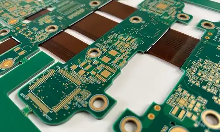
In a world increasingly dependent on compact, high-performance electronics, 10 Layer Rigid-flex PCBs are proving to be indispensable. Their unique combination of rigid and flexible layers enables designs that were previously thought unattainable. Whether you’re crafting medical devices, military hardware, or cutting-edge wearable technology, these advanced circuits provide the foundation for exceptional performance and reliability.
In this comprehensive guide, we delve into the core aspects of rigid-flex PCB manufacturing, including advanced design techniques, material science breakthroughs, and our unmatched expertise in delivering reliable, high-layer-count solutions. Whether you’re a seasoned designer or exploring rigid-flex technology for the first time, this resource will equip you with the insights and strategies needed to bring your most ambitious projects to life.
What Sets 10 Layer Rigid-flex PCBs Apart from Traditional Designs?
In today’s tech world, human are constantly faced with the challenge of designing electronics that meet stringent performance standards without compromising on space, reliability, or cost. Enter the 10 Layer Rigid-flex PCB. These advanced circuit boards are reshaping the electronics industry by providing a unique blend of rigidity and flexibility, offering both structural integrity and adaptability that traditional designs simply can’t match.
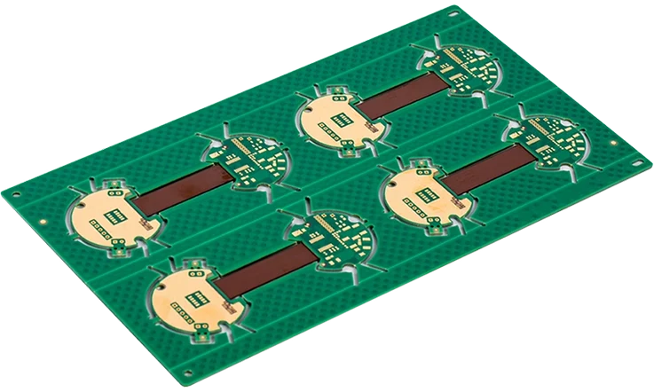
Rigid-flex PCBs bring versatility to the table. They are a hybrid solution that allows us to integrate multiple layers of rigid and flexible substrates in a single circuit. This hybridization is a major advantage when working with compact, high-performance devices such as military systems, wearable technology, and medical equipment, where the assembly and design need to fit into tight spaces while maintaining top-tier reliability.
Integrating Rigid and Flexible Layers for Complex Assemblies
The ability to combine rigid and flexible layers in one PCB eliminates the need for separate connectors and cables that are typically used in traditional designs. This not only reduces the physical footprint of the board but also helps to simplify the assembly process. By integrating everything into a single unit, the design eliminates potential points of failure, making the end product more durable and reliable.
●For example, you’re designing a system for aerospace applications. In these high-stakes environments, every connection needs to be strong and resilient. Using rigid-flex PCBs, you can achieve this by integrating flexible sections that fold and bend to fit into compact spaces while maintaining the electrical integrity of the rigid layers. This eliminates the risk of breakage at connection points and helps to avoid the need for extra assembly steps, such as the use of connectors that can wear out over time.
In contrast, traditional rigid PCBs might require additional space to accommodate connectors and cables, making the design process more complex and costly. With a rigid-flex PCB, you can reduce component count and ensure the system is less prone to failure due to mechanical stress.
High-density Interconnects for Enhanced Functionality
A standout feature of 10 Layer Rigid-flex PCBs is their ability to handle high-density interconnects (HDI). These designs incorporate multiple layers of fine traces, allowing for more complex circuitry within a compact space. This is achieved through advanced stack-up configurations such as the 4+2+4 layer structure, which ensures that the board can carry more signals without increasing the overall size.
●Take medical imaging systems like MRI or CT machines, where the demand for high-speed data transmission is non-negotiable. Employing a 10-layer rigid-flex PCB equipped with HDI technology ensures seamless operation by maintaining pristine signal quality, even under the rigorous demands of real-time imaging. This advanced configuration prevents issues like signal loss or interference, paving the way for consistently clear and accurate diagnostic outputs. With such a setup, these systems can handle massive data loads efficiently, keeping everything in tip-top shape while performing under pressure.
Moreover, High-density interconnects are a powerhouse for applications demanding ultra-fast signal processing, such as military-grade communication systems or cutting-edge 5G networking gear. The compact layering enables quicker data transfer while keeping interference to a bare minimum.. The tightly packed layers allow for faster data transfer with less interference, all while minimizing the PCB’s overall size—ideal for applications where real estate is limited, and performance can’t be compromised.
Material Selection that Matches Performance Demands
When it comes to the performance of a 10-layer rigid-flex PCB, the right material choice is non-negotiable. We handpick substrates and laminates tailored to each device’s specific demands. For high-speed applications, materials like low-loss laminates and thermally stable substrates are go-to options to ensure signal integrity, even when the environment gets tough.
●For example, In the medical sector, where accuracy and reliability are a must, using high-quality laminates helps ensure the PCB functions consistently over time, even under demanding conditions. In wearable electronics, where both flexibility and strength are necessary, flexible materials such as polyimide are used for the flexible layers, allowing the PCB to bend and adapt. Meanwhile, rigid materials like FR4 or Rogers are employed for the rigid layers, offering the durability needed to support electrical performance. This careful selection of materials provides a balance between flexibility and stability, allowing the circuits to conform to the body while maintaining their intended electrical functions.
Thermal management is another factor in material selection. Rigid-flex PCBs are designed with thermal dissipation in mind, using materials that can handle heat without compromising the board’s performance. For instance, aerospace systems that operate in extreme temperature variations can rely on these boards to maintain performance without overheating, thanks to the use of thermally conductive materials and advanced fabrication techniques.
Advanced Design Techniques for 10 Layer Rigid-flex PCBs
The rising demand for cutting-edge electronics has driven innovation in PCB design, particularly for 10-layer rigid-flex configurations. These advanced design methods cater to the exacting standards of industries such as aerospace, healthcare, and wearable technology. By incorporating precise engineering approaches, these PCBs deliver the reliability and performance needed to handle the challenges of modern applications. With our engineers constantly exploring new possibilities, these strategies provide a solid foundation for creating products that stand out in fiercely competitive markets.
The integration of rigid and flexible circuits in a 10-layer stack-up provides a unique approach that addresses the need for miniaturization, durability, and complex functionalities in one package. To achieve the best results, advanced techniques must be applied across several aspects, including signal integrity, thermal management, and simplifying the assembly process.
Impedance Control and Signal Stability
Maintaining consistent and accurate signal transmission is a core requirement in high-speed applications. With 10-layer rigid-flex PCBs, designs are tailored to perform flawlessly in scenarios where any signal disruption could lead to compromised functionality. Whether it’s powering wearable devices that monitor critical metrics, driving advanced medical diagnostic systems, or supporting secure military communications, these PCBs are crafted to ensure precision at every turn. The meticulous design ensures seamless performance, even in demanding environments, making them a go-to choice for applications where reliability is a must.
Achieving Precision in Impedance Matching-
Impedance matching is the process of ensuring that the electrical impedance of a trace matches the characteristic impedance of the transmission line. Any deviation in this impedance can result in signal reflections, which in turn lead to data loss, noise, or errors in the transmission. In a multilayer PCB like a 10 Layer Rigid-flex design, this is particularly challenging due to the interaction of both rigid and flexible layers.
To achieve precise impedance matching, we must rely on advanced techniques such as the use of controlled impedance traces, coupled with the correct selection of materials. The most common materials used to control impedance are specialized laminates with consistent dielectric constants, such as Teflon or other low-loss materials, which ensure that the signals remain stable even at high frequencies.
Signal Integrity Considerations in Multilayer Configurations-
In multilayer PCBs, the signal integrity must be maintained across the various layers, as interference from neighboring traces can lead to crosstalk. In 10 Layer Rigid-flex PCBs, ground planes and power planes are strategically placed to shield the sensitive signal layers, thereby reducing the chances of signal interference and noise.
The incorporation of blind and buried vias enhances signal routing by shortening pathways and minimizing unnecessary crossovers. This thoughtful design approach optimizes signal flow and significantly reduces potential distortion, ensuring smooth performance even under demanding conditions. By carefully managing signal paths and layering, these PCBs deliver the performance edge needed to handle intricate and high-speed applications with finesse.
Impedance Control Techniques for 10 Layer Rigid-flex PCBs-
| Technique | Description | Advantages | Common Applications |
| Controlled Impedance Traces | Ensuring consistent impedance across the board. | Reduces signal reflection. | High-speed data transfer systems, medical devices. |
| Use of Ground and Power Planes | Provides shielding to sensitive signals. | Minimizes noise and crosstalk. | Aerospace, military electronics. |
| Blind and Buried Vias | Routing signals more efficiently. | Reduces signal path length. | Wearables, complex medical devices. |
Thermal Management in Multilayer Designs
As electronic devices become more powerful, tackling heat dissipation becomes a major design focus. For 10 Layer Rigid-flex PCBs, maintaining consistent thermal management across the board safeguards against overheating, which can lead to damaged components, system instability, or reduced performance.
Managing Heat in Complex PCB Designs-
In aerospace or military systems, where components are often subjected to harsh environmental conditions, managing thermal load is essential. 10 Layer Rigid-flex PCBs are designed with heat dissipation strategies in mind, particularly for components that generate a significant amount of heat. The multilayer structure of these boards allows for optimal routing of thermal vias, copper pours, and heat sinks that help dissipate heat away from sensitive components.
The use of materials such as thermally conductive copper, aluminum, or composite materials like ceramic-filled epoxies ensures that the thermal conductivity of the PCB is maximized. Additionally, We take into account the thermal expansion properties of both rigid and flexible layers to prevent warping or delamination during thermal cycling.
Thermal Stability for Wearables and Medical Devices-
In wearable devices, managing heat is a balancing act between performance and user comfort. The heat generated by the board must be dissipated without compromising comfort or performance. By selecting flexible, high-temperature-resistant materials, such as polyimide, and integrating them into the PCB design, we can ensure that the device continues to operate reliably without overheating.
Thermal Management Techniques for 10 Layer Rigid-flex PCBs-
| Technique | Description | Advantages | Common Applications |
| Use of Thermal Vias | Allows for heat dissipation through layers. | Prevents thermal damage. | Aerospace, military electronics. |
| Copper Pour for Heat Sinks | Strategically places copper for heat dissipation. | Maximizes thermal conductivity. | Wearables, medical electronics. |
| Polyimide for Flexibility | High-temperature resistant material. | Maintains flexibility and strength under high heat. | Wearable electronics, industrial sensors. |
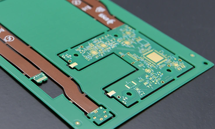
Reducing Assembly Complexity with Flexible Design
One of the main advantages of 10 Layer Rigid-flex PCBs is their ability to streamline assembly processes by eliminating the need for connectors, cables, and external components. By integrating flexible layers directly into the PCB, we are able to create compact and reliable designs that are easier to assemble and maintain.
Simplifying the Assembly Process-
In traditional PCBs, connectors and cables are often necessary to link various sections of the board together. These external components can be time-consuming to assemble and prone to failure due to wear and tear. However, by using flexible circuits within the 10-layer stack-up, much of this complexity can be avoided. The flexible segments allow the PCB to be bent or shaped to fit the necessary form factor, eliminating the need for additional interconnects.
This design flexibility also leads to reduced manufacturing costs, as fewer components and connections are required. The overall result is a more cost-efficient assembly process that doesn’t sacrifice performance or reliability.
Enhancing Reliability Through Fewer Connections-
With fewer points of failure, 10 Layer Rigid-flex PCBs offer enhanced reliability, especially in industries like aerospace or military, where failure is not an option. Each connection in a traditional design represents a potential point of failure, whether it’s a loose connector or a cable that is subject to wear over time. By reducing the number of connections, we ensure that the board remains durable and resistant to environmental stress.
Reducing Assembly Complexity with Flexible Design-
| Technique | Description | Advantages | Common Applications |
| Elimination of Connectors | Direct integration of flexible circuits into the PCB. | Reduces complexity and cost. | Aerospace, medical devices. |
| Flexible Design for Shape Adaptation | Allows the PCB to conform to the device shape. | Eliminates the need for external connectors. | Wearable electronics, industrial sensors. |
| Simplified Manufacturing | Fewer parts required for assembly. | Streamlines the assembly process. | Military, aerospace. |
This approach to 10 Layer Rigid-flex PCB design reduces the assembly complexity and increases the reliability of the final product. By eliminating the need for connectors and cables, the design becomes more robust and easier to manufacture—without sacrificing performance.
Structure and Design of a 10 Layer Rigid-flex PCB
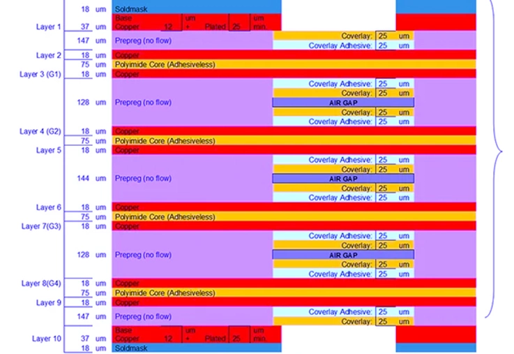
The design of a 10-layer rigid-flex PCB is a masterclass in engineering precision, blending the durability of rigid sections with the versatility of flexible layers. This layered construction alternates between rigid and flexible materials, meticulously arranged to meet the diverse needs of advanced electronic systems. The result is a circuit board that holds up under pressure while adapting to challenging layouts and space constraints.
Layer Stack-up: Striking the Perfect Balance
The design of a 10-layer rigid-flex PCB begins with a carefully calculated stack-up to harmonize electrical, mechanical, and thermal properties.
●Composition: The structure alternates between rigid and flexible layers to meet specific application needs.
●Layer Thickness: Each layer’s thickness is tailored to optimize durability and functionality.
●Material Selection: Common materials include FR-4 for rigid layers and polyimide for flexible substrates.
Example of a 10-Layer Stack-up-
| Layer | Type | Material | Function |
| 1 | Rigid | FR-4 | Component Mounting & Signal |
| 2 | Flexible | Polyimide | Bendable Signal Traces |
| 3-6 | Alternating | Copper/Polyimide | Signal and Ground Paths |
| 7-10 | Rigid | FR-4 | Power Planes & Structural Support |
Rigid Layers: Foundation and Functionality
Rigid layers serve as the structural backbone, offering support for components and housing essential circuitry.
●Material Choice: FR-4 laminate is the gold standard due to its mechanical and electrical properties.
●Component Mounting: Components such as ICs, resistors, and capacitors are soldered onto these layers.
●Copper Layers: These layers handle signal transmission and power distribution.
Key Design Tip: Ensure optimal spacing between traces on rigid layers to prevent short circuits and maintain signal fidelity.
Flexible Layers: Bridging Design Challenges
Flexible layers bring versatility, allowing the PCB to adapt to confined spaces or dynamic environments.
●Material Characteristics: Polyimide substrates ensure durability under repeated flexing.
●Applications: Ideal for dynamic bending in wearable devices and compact assemblies in satellites.
●Signal Paths: Copper traces on flexible layers maintain uninterrupted connectivity.
Via Structures: Connecting the Layers
Vias facilitate electrical interconnections across rigid and flexible layers.
●Through-hole Vias: Extend through all layers for robust connectivity.
●Blind Vias: Link outer layers to selected inner layers, conserving space.
●Buried Vias: Enable inner-layer connections without penetrating the surface.
Types of Vias and Their Usage-
| Via Type | Purpose | Advantages |
| Through-hole | Multi-layer Connectivity | Strong mechanical bonding |
| Blind Vias | Space-saving in compact designs | Reduces routing congestion |
| Buried Vias | Internal Layer Connections | Minimizes surface clutter |
Signal Routing: Ensuring High-performance Connectivity
Signal integrity is core need in rigid-flex PCB design.
●Impedance Matching: Achieved through precise trace width and spacing calculations.
●High-speed Design: Differential pairs and shielding reduce EMI and crosstalk.
●Routing Guidelines: Isolate high-speed signals from power traces to maintain clarity.
Mechanical Design Considerations
Engineering the mechanical aspects ensures durability and reliability.
●Bend Radii: Design with ample bending radius to prevent stress fractures.
●Stiffeners: Used to reinforce fragile areas prone to mechanical strain.
●Support Structures: Added in critical zones to ensure long-term durability.
Pro Tip: Use 3D modeling software during the design phase to visualize folding and bending areas.
This professional approach to designing 10-layer rigid-flex PCBs ensures robust performance while meeting the specific needs of high-tech industries. So, The structure and design of a 10 layer rigid-flex PCB demand careful consideration of electrical, mechanical, and manufacturing aspects. By balancing these factors, we can create a reliable and versatile circuit board that meets the specific requirements of the intended application.
H2: Design Considerations for 10 Layer Rigid-flex PCB
Designing 10 layer rigid-flex PCBs requires a deep understanding of the unique challenges that come with integrating rigid and flexible substrates into a multi-layer configuration. Below are key design factors to consider for a successful 10 layer rigid-flex PCB.
Layer Stack-up: Planning for Structural Integrity
The layer stack-up is the foundation of a rigid-flex PCB and dictates how the different layers will interact. Choosing the right configuration of rigid and flexible layers ensures that the PCB can meet both mechanical and electrical requirements. For a 10 layer design, the order and arrangement of layers need careful attention.
Planning the Rigid and Flex Layers-
In a 10-layer rigid-flex PCB, the stack-up typically includes alternating rigid and flexible layers. This design allows the flexible areas to bend while maintaining the structural stability of the rigid sections. The rigid layers are often used for high-density component placement, while the flexible layers accommodate areas that require movement or complex shapes.
Optimizing Power and Ground Planes-
When planning the layer stack-up, it’s also important to consider the placement of power and ground planes. These planes should be distributed evenly throughout the design to reduce electromagnetic interference (EMI) and maintain signal integrity. Proper placement of these planes can minimize noise and ensure that the PCB performs well under high-speed conditions.
Typical Layer Stack-up for 10 Layer Rigid-flex PCB-
| Layer Number | Type | Description |
| 1 | Rigid | Component placement, signal traces |
| 2 | Flex | Flex material layer for bending |
| 3 | Rigid | Power/ground plane |
| 4 | Flex | Signal routing layer, flexible zone |
| 5 | Rigid | Component placement, signal traces |
| 6 | Rigid | Power/ground plane |
| 7 | Flex | Flex zone for connectivity |
| 8 | Rigid | Component placement, signal traces |
| 9 | Flex | Flex zone for bending and routing |
| 10 | Rigid | Structural reinforcement, component placement |
Bend Areas and Flexibility: Defining Movement Zones
Flexibility is one of the key benefits of rigid-flex PCBs, but it also introduces potential points of failure if not properly designed. The bend areas must be carefully planned to prevent over-stress on components and PCB traces.
Designing Flex Areas-
The flexibility of a rigid-flex PCB hinges on the choice of materials and the bend radius design. Materials like polyimide are a popular pick for the flexible sections, thanks to their durability and resilience under repeated bending. Getting the bend radius right is a non-negotiable step in the process—if it’s too tight, the risk of mechanical stress increases, which could lead to wear and tear or outright failure. By dialing in the proper specifications for these bend areas, we ensure the PCB can handle the twists and turns without breaking a sweat, offering a long-lasting and dependable performance.
Stress Considerations-
Placing components in areas where bending occurs can lead to physical strain. Therefore, sensitive components like ICs, connectors, and large capacitors should be strategically placed away from these bend zones. This placement avoids issues like microcracks in the solder joints or damage to the component itself.
Minimum Bend Radii for Flexible PCBs-
| Material Type | Minimum Bend Radius (mm) | Recommended Application |
| Polyimide | 5 | Flexible zone, wearable devices |
| FR-4 | 10 | Rigid zones, non-flexing areas |
| Liquid Crystal Polymer (LCP) | 7 | Medical, aerospace devices |
Component Placement: Strategically Placing for Performance
Component placement on a 10 layer rigid-flex PCB is a delicate balancing act between electrical performance, mechanical design, and manufacturability. Components must be placed where they can function optimally while avoiding areas that may be subject to mechanical stress due to flexing.
Considerations for Flexing Zones-
While placing components in rigid zones is straightforward, the flexible zones require additional consideration. For example, tall components or those with large footprints may not be suitable for flexible areas because they can bend or be damaged during movement. Ensuring that there is enough clearance between components is essential to prevent interference or mechanical strain.
Avoiding Bending Stress-
Additionally, keep in mind that components close to the bend area should have enough room to avoid mechanical stress. Using stiffeners or reinforcements in these areas can help protect sensitive components and ensure long-term durability.
Signal Routing: Optimizing Performance and Minimizing Interference
Maintaining clean signal paths in 10-layer rigid-flex PCBs is a must, especially for high-speed systems where even minor hiccups can ripple through performance. Thoughtful routing of signal traces helps sidestep common pitfalls like electromagnetic interference (EMI), signal loss, and crosstalk. By sticking to best practices in trace layout and layering, we can dodge these headaches and keep the data flow steady and reliable. It’s all about designing a board that plays nice with high-frequency signals, even when the stakes are high and the margins for error are slim.
Minimizing Signal Propagation Delays-
To optimize signal routing, we should consider trace lengths, impedance matching, and the separation of high-speed signals from noisy or power-heavy traces. Using differential signaling where applicable can help enhance the PCB’s ability to handle high-frequency signals with minimal degradation.
Separating Signal Traces-
When designing high-speed circuits, it’s necessary to keep sensitive signal traces away from power or ground traces. This approach helps minimize interference and reduces cross-talk between traces. By carefully planning the layout and ensuring proper spacing, we can improve the clarity and reliability of signals across the PCB. With attention to these details, the design can avoid potential disruptions, ensuring that the system functions as intended with solid, uninterrupted performance.
Signal Trace Routing Guidelines-
| Trace Type | Minimum Trace Width (mil) | Recommended Spacing (mil) | Application |
| High-speed Signal | 4 | 6 | RF, telecom, medical devices |
| Power/ground traces | 8 | 10 | Power distribution, low noise |
| Differential pairs | 6 | 10 | High-speed data transmission |
Via Placement: Ensuring Structural and Electrical Integrity
Via placement in a 10 layer rigid-flex PCB is a another aspect of both electrical connectivity and mechanical design. Vias must be placed in such a way that they don’t interfere with the flexible areas or introduce impedance mismatches.
Minimizing Via Stress-
Vias should not be located in areas that will be subjected to repeated bending, as this can cause mechanical stress and lead to failure. Additionally, excessive via use can introduce signal loss, so they should be used sparingly and only where necessary.
Via Technology Considerations-
Advanced via technologies, like microvias or blind/buried vias, can be employed to minimize space usage and ensure reliable electrical connections across layers without compromising flexibility.
Via Placement Guidelines for Rigid-flex PCBs-
| Via Type | Application | Advantages |
| Microvia | High-density interconnects | Small form factor, less space |
| Blind/Buried Vias | Multi-layer connections | Reduces stress and impedance |
| Through-hole Vias | Rigid layers, power distribution | Reliable, easy to fabricate |
Design for Manufacturing (DFM): Ensuring Feasibility
Design for Manufacturability (DFM) is a major consideration in PCB design, especially when dealing with 10-layer rigid-flex PCBs. To ensure the design can be successfully manufactured, so we must to consider factors like trace width, via size, and spacing tolerances. Keeping these points in mind from the beginning helps align the design with manufacturing capabilities, leading to a smoother production process and minimizing unexpected challenges.
Aligning Design with Manufacturing Capabilities-
Ensure that the PCB design is well within the capabilities of the manufacturing process, including the use of appropriate trace widths and spacing. Designs that push the limits of manufacturing tolerances may encounter difficulties in fabrication or assembly.
Thermal Management: Handling Heat Dissipation
Thermal management is often something that flies under the radar in PCB design, but for 10-layer rigid-flex PCBs, it’s a whole different ball game. With high-density components packed tightly on the board, managing heat flow becomes a big deal. If the heat isn’t dealt with properly, things can heat up pretty fast, leading to performance drops or even component failure. Proper heat dissipation techniques, such as using thermal vias and heat sinks, help keep the system running without hitting the boiling point.
Utilizing Thermal Vias and Heat Sinks-
Thermal vias can be placed in areas with high thermal load to help distribute heat across the PCB. Additionally, integrating heat sinks or thermal pads in strategic locations ensures that temperature-sensitive components remain within their operating limits.
Compliance with Industry Standards: Meeting Global Requirements
Ensure that your design adheres to relevant industry standards like IPC-2223 and IPC-6011/6012 for flexible and rigid PCBs, respectively. Compliance ensures the product meets safety and performance requirements and is suitable for high-quality, reliable production.
Manufacturing Excellence in 10 Layer Rigid-flex PCBs
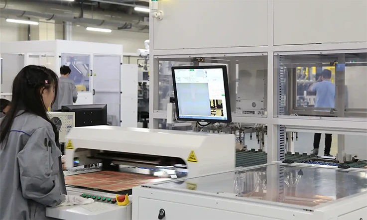
Creating a high-quality 10 Layer Rigid-flex PCB involves far more than just the design phase. It requires mastering sophisticated manufacturing processes that can handle the complex requirements of these advanced boards. With applications spanning industries such as aerospace, medical devices, wearables, and military, precision and durability are non-negotiable. Manufacturing excellence is achieved by focusing on prototyping, advanced fabrication processes, and rigorous quality assurance. Each of these steps ensures that the final product meets the expectations for reliability, performance, and compliance with industry standards.
Prototyping for Complex Designs
Prototyping acts as a stepping stone from design to large-scale production, providing a chance to fine-tune and validate intricate PCB designs. This step is especially valuable for 10 Layer Rigid-flex PCBs, where the interplay of multiple layers and the combined rigid and flexible sections demands thorough testing for both functionality and dependability. It’s like taking a new recipe for a test run—ensuring the ingredients work well together and the final result meets expectations. By putting prototypes through their paces, we can uncover and address potential issues, ensuring a seamless path to manufacturing without second-guessing the final product.
Rapid Prototyping to Validate Design and Optimize Performance-
Tackling the challenges of multilayer rigid-flex boards means making sure every design element works harmoniously when brought together. Prototyping acts as the go-to method for ironing out potential issues, offering a hands-on model to evaluate signal integrity, heat dissipation, and structural durability before committing to large-scale production. It’s like test-driving a car—you get to fine-tune the performance, ensure reliability, and catch any hiccups before hitting the assembly line. By iterating through prototypes, we can troubleshoot and refine designs, setting the stage for a smooth transition to manufacturing without unexpected surprises.
By using rapid prototyping technologies like additive manufacturing or laser-cutting methods, we can create precise physical models of the design. These models allow us to test and modify the design in real-time, saving both time and costs in the long run.
Addressing Challenges in Multilayer Fabrication-
Creating a 10-layer rigid-flex PCB requires stacking multiple layers of flexible and rigid materials with pinpoint accuracy to ensure everything lines up just right. During the manufacturing process, this alignment is what keeps the circuitry intact and the board functioning seamlessly from edge to edge. Proper bonding of these layers not only guarantees electrical connections stay solid but also prevents warping or misalignment that could throw a wrench into the final performance. It’s like building a skyscraper—every layer needs to sit perfectly on the one below to hold up under pressure and deliver reliable results.
Prototyping is an essential tool in addressing alignment challenges. It provides a hands-on way to ensure that the PCB design can be manufactured to meet dimensional tolerances and material requirements. This step helps to identify potential issues, such as layer misalignment, incorrect vias, or thermal expansion concerns, before they can affect the final product.
Prototyping for 10 Layer Rigid-flex PCBs-
| Technique | Description | Advantages | Common Applications |
| Additive Manufacturing | Creates quick, low-cost models for testing. | Saves time and reduces early-stage errors. | Aerospace, medical devices. |
| Laser Cutting and Drilling | High precision drilling for multilayer boards. | Improves accuracy and minimizes waste. | Wearables, military electronics. |
| High-Fidelity Testing | Real-world testing on prototype designs. | Ensures design integrity and functionality. | Medical, avionics. |
Advanced Fabrication Processes
The fabrication of 10 Layer Rigid-flex PCBs requires the use of high-precision manufacturing techniques to ensure both performance and durability. The process involves various steps that must be executed with careful attention to detail, as even minor errors can result in suboptimal performance or failure of the final product.
Precision Techniques Like Laser Drilling, Plating, and Lamination-
Laser drilling stands out as one of the sharpest tools in the shed for creating vias in multilayer boards, especially when working on designs that mix rigid and flexible sections. This method delivers ultra-precise hole creation, ensuring even the tiniest vias are formed with spot-on accuracy. In 10-layer rigid-flex designs, where vias must pass through multiple layers, laser drilling offers unmatched precision that keeps everything aligned like clockwork. By maintaining tight tolerances, this technique helps avoid misalignment issues, ensuring the final product performs exactly as intended.
Plating is another process in PCB fabrication, where copper plating is applied to the drilled vias to create reliable electrical connections between layers. The plating process needs to be done uniformly to prevent weak points that could cause electrical failure or performance degradation.
Lamination is used to bond multiple layers of material into a single structure. For 10 Layer Rigid-flex PCBs, this process must ensure that the flexible and rigid layers bond seamlessly, allowing the board to perform as a single unit without compromising on flexibility or durability.
Importance of Maintaining Alignment in Multilayer Structures-
One of the most challenging aspects of multilayer fabrication is ensuring that all the layers align perfectly throughout the entire manufacturing process. The layers must bond correctly, the vias must be drilled accurately, and the electrical traces must align precisely across the layers. Misalignment can cause problems such as short circuits, open circuits, and poor signal integrity, all of which can lead to system failures.
Advanced alignment techniques, such as optical alignment systems, are used to ensure that each layer is positioned correctly before and during lamination. This level of precision is necessary for 10 Layer Rigid-flex PCBs, where the need for exact alignment increases due to the complexity of combining rigid and flexible layers.
Advanced Fabrication Techniques for 10 Layer Rigid-flex PCBs-
| Technique | Description | Advantages | Common Applications |
| Laser Drilling | Precise drilling for vias in multilayer designs. | Ensures small, accurate vias. | Medical devices, aerospace. |
| Copper Plating | Electroplating copper onto vias. | Ensures electrical connections are reliable. | Military electronics, wearables. |
| Multi-layer Lamination | Bonding multiple layers with controlled pressure and temperature. | Ensures seamless integration of rigid and flexible layers. | High-performance electronics. |
Quality Assurance Standards
In industries such as aerospace, military, and medical devices, the reliability and safety of electronic components cannot be compromised. To meet these high demands, manufacturers of 10 Layer Rigid-flex PCBs adhere to strict quality assurance standards, ensuring that every product is tested for performance, durability, and compliance.
Meeting ISO, IPC Class 3, and Military-Grade Certifications-
To guarantee quality, we need follow international standards such as ISO 9001 for quality management and IPC-6012 Class 3 for the production of high-reliability PCBs. For military applications, the boards must also meet the military standards for ruggedness, reliability, and performance, often involving additional certifications such as MIL-PRF-31032.
These standards ensure that every PCB is capable of performing in the most demanding conditions, such as extreme temperatures, humidity, and vibration. They also require rigorous testing to ensure that the boards will continue to function reliably over the course of their lifespan.
Comprehensive Testing for Reliability and Durability-
Throughout the production process, thorough testing ensures the final product aligns with the required specifications. This process includes everything from visual inspections to catch surface flaws, to rigorous electrical tests that verify circuit continuity and functionality. Environmental assessments and thermal cycling are also carried out, mimicking real-world conditions to see how the PCBs handle temperature swings and other stressors. By diving deep into testing at every stage, potential hiccups are identified early, allowing for adjustments that guarantee the boards perform without a hitch once they’re put to work in their final applications.
Quality Assurance Testing for 10 Layer Rigid-flex PCBs-
| Technique | Description | Advantages | Common Applications |
| Visual Inspection | Checking for physical defects and alignment. | Quickly detects manufacturing errors. | Medical, military electronics. |
| Electrical Testing | Ensuring all electrical connections are intact. | Confirms electrical integrity. | Aerospace, wearables. |
| Environmental Testing | Simulating environmental conditions. | Ensures durability under extreme conditions. | Industrial sensors, military. |
Material Science for 10 Layer Rigid-flex PCBs
When designing 10-layer rigid-flex PCBs, the selection of materials directly impacts the performance and durability of the final product. These advanced boards are often deployed in settings where conventional PCB materials fall short. We need to weigh factors such as high-frequency signal handling, mechanical strength, and heat tolerance to ensure the materials align with the application’s demands. As material science continues to evolve, advancements in PCB manufacturing are expected to bring more efficient designs, greater adaptability, and eco-friendly solutions into play. It’s a field that keeps pushing the envelope, with new innovations setting the stage for what’s next in electronics.
High-frequency Materials for Signal Performance
When designing high-performance 10 Layer Rigid-flex PCBs, the materials selected directly impact signal integrity, especially at high frequencies. Applications such as medical imaging systems, aerospace radar, and high-speed telecommunications demand materials that can transmit signals without significant loss or distortion. This requires materials engineered specifically to minimize signal degradation, even at frequencies well above standard levels.
How Materials like Megtron-6 Improve High-speed Signal Transmission-
Megtron-6, a high-frequency laminate material, has emerged as a go-to choice for engineers working with demanding high-speed designs. Megtron-6 offers a low dielectric constant and low dissipation factor, making it ideal for signal integrity in high-speed circuits. It provides an effective solution for complex applications, including 10 Layer Rigid-flex PCBs, by minimizing the signal loss during transmission.
Materials like Megtron-6 ensure that the signal performance remains reliable, even under the intense environmental and operational conditions typically encountered in aerospace, medical devices, and other applications.
Importance of Low-loss Materials in Advanced Applications-
In 10-layer rigid-flex PCB designs, selecting low-loss materials is a smart move for preserving the quality of high-frequency signals. These materials reduce energy dissipation as signals pass through the board, maintaining signal clarity. Options like PTFE (Polytetrafluoroethylene) and LCP (Liquid Crystal Polymer) are widely used for their ability to minimize signal loss and provide exceptional electrical performance. Their characteristics make them well-suited for applications where signal reliability is non-negotiable.
High-frequency Materials for 10 Layer Rigid-flex PCBs-
| Material | Dielectric Constant | Loss Factor | Ideal Application |
| Megtron-6 | 3.55 | Low | High-speed telecom, aerospace, medical |
| PTFE (Teflon) | 2.1 – 2.3 | Very Low | High-frequency signal transmission |
| Liquid Crystal Polymer (LCP) | 2.5 – 3.0 | Very Low | Flexible PCBs, wearables, automotive |
Enhancing Durability with Thermal-resistant Materials
Durability is a core requirement in high-performance 10 Layer Rigid-flex PCBs, especially when used in extreme environments such as aerospace and military applications. These boards need to withstand high thermal stresses while maintaining their structural integrity. For this reason, materials with exceptional thermal resistance are required to ensure longevity and consistent performance.
Key Features of Materials for Aerospace and Military Applications-
In aerospace and military settings, thermal resistance takes center stage, as circuit boards need to endure wide-ranging temperature swings while maintaining consistent performance. Materials like ceramic-filled PTFE and polyimide offer significant thermal stability, making them suitable for these demanding applications. These materials are engineered to withstand the extreme conditions found in space, high-altitude operations, and harsh battlefield environments.
For example, Polyimide, a flexible and heat-resistant polymer, is a go-to material for flexible layers in 10-layer rigid-flex PCBs. Its ability to stay stable under intense heat makes it a solid choice for designs that need to handle challenging thermal conditions. Applications like radar systems or aircraft electronics often push the limits of heat dissipation, and polyimide’s resilience helps these boards keep up without breaking a sweat.
Strategies for Minimizing Wear and Tear-
As with thermal resistance, minimizing wear and tear is a challenge that we face when designing PCBs for aerospace or military applications. Materials like polyimide are favored for their ability to resist degradation under high thermal cycling. Additionally, advanced protective coatings such as gold or silver plating can be applied to increase the durability of critical areas like contact pads and vias, protecting them from oxidation and wear over time.
Thermal-resistant Materials for 10 Layer Rigid-flex PCBs-
| Material | Thermal Conductivity | Temperature Range (°C) | Ideal Application |
| Polyimide | 0.3 W/m·K | -200 to 250 | Aerospace, military, automotive |
| Ceramic-filled PTFE | 0.5 W/m·K | -50 to 200 | Military, high-performance avionics |
| Polyphenylene Sulfide (PPS) | 0.3 W/m·K | -50 to 220 | Harsh industrial environments |
Innovations in PCB Material Technology
As the demand for higher performance, more compact, and eco-friendly electronics grows, innovations in PCB material technology are rapidly changing the industry. These innovations are not only improving performance but also contributing to environmental sustainability.
Emerging Trends in Low-loss, Eco-friendly, and Flexible Materials-
Low-loss materials are at the forefront of innovation, offering both excellent signal integrity and reduced environmental impact. For example, bio-based laminates and recyclable thermoset polymers are beginning to replace traditional materials in the production of Rigid-flex PCBs. These materials offer lower environmental impact without compromising performance. Additionally, the demand for flexible PCBs that are lightweight and can be used in wearable electronics is pushing us to explore new materials that can handle high-density designs while remaining flexible.
Predictions for Next-generation PCB Materials-
We can expect to see more advanced materials that combine high-performance with sustainability. Materials like graphene and carbon nanotubes are on the horizon for use in PCBs due to their excellent electrical conductivity and flexibility. These materials are predicted to revolutionize PCB technology by enabling faster signal transmission and creating thinner, more compact designs.
Next-generation PCB Materials for 10 Layer Rigid-flex PCBs-
| Material | Electrical Conductivity | Environmental Impact | Ideal Application |
| Graphene | Very High | Low | High-performance, flexible PCBs |
| Bio-based Laminates | Moderate | Low | Eco-friendly electronics, wearables |
| Carbon Nanotubes | Extremely High | Low | High-speed, lightweight applications |
Why Choose Us?
Top Rigid-flex PCB Manufacturer and Supplier in China!
When it comes to manufacturing rigid-flex PCBs, selecting the right partner can significantly impact the success of your project. Our company stands out by offering advanced manufacturing capabilities, stringent quality control, competitive pricing, and efficient delivery timelines. Here’s why we are the ideal partner for your rigid-flex PCB needs:
1.Unmatched Expertise and Advanced Capabilities
With extensive experience in the PCB manufacturing industry, we excel in creating intricate rigid-flex designs that cater to diverse industries such as aerospace, medical devices, automotive, and consumer electronics. Our facilities are equipped with cutting-edge technology, including precision laser drilling and advanced lamination processes, ensuring top-tier performance and reliability.
2.Provide 4-46 Layer Rigid-Flex PCB Manufacturing
We specialize in fabricating rigid-flex PCBs with complex layer counts, ranging from 4 layers to as many as 46 layers, accommodating intricate and high-density designs. Our advanced manufacturing processes allow seamless integration of multiple layers while maintaining optimal electrical performance.
| Layer Range | Applications |
| 4-12 Layers | Consumer electronics, IoT devices |
| 12-24 Layers | Automotive, medical equipment |
| 24-46 Layers | Aerospace, military, data centers |
These capabilities empower us to handle even the most demanding projects with precision and reliability.
3.Commitment to Superior Quality
Quality forms the foundation of everything we do. Our rigid-flex PCBs meet and exceed industry standards, such as IPC Class 3 and ISO certifications. Each product undergoes rigorous testing, including electrical continuity checks, impedance analysis, and thermal stress evaluations, ensuring flawless performance.
| Testing Method | Purpose |
| Automated Optical Inspection | Identifying visual defects |
| X-Ray Inspection | Ensuring layer alignment |
| Flying Probe Testing | Verifying electrical integrity |
4.Manufacturing Using Renowned PCB Materials
We provide expertise in working with high-quality materials from globally recognized brands such as Isola, Rogers, Taconic, and Panasonic. Our proficiency ensures compatibility with advanced applications, including high-frequency, thermal management, and eco-friendly requirements.
| Material Brand | Features |
| Rogers | Low-loss, high-frequency performance |
| Isola | Excellent thermal resistance |
| Taconic | Eco-friendly and cost-effective solutions |
| Panasonic | High-reliability and durability in flex PCBs |
Our familiarity with these materials allows us to tailor solutions for specialized needs while maintaining exceptional quality.
5.Competitive Pricing Without Compromise
We strike the perfect balance between affordability and quality. By leveraging cost-efficient production methods and material sourcing, we offer competitive pricing without sacrificing performance or reliability. Our transparent pricing model eliminates hidden fees, making us a trustworthy partner.
6.Fast and Reliable Delivery
Time is of the essence, and we ensure timely delivery to meet your project deadlines. With optimized workflows and an experienced logistics team, we support fast turnarounds for both prototypes and mass production.
| Service Type | Turnaround Time |
| Prototype Manufacturing | As fast as 5 days |
| Standard Production | 7–10 days |
| Expedited Delivery | Available upon request |
7.Comprehensive Customer Support
We are with you every step of the way, offering expert guidance during the design phase, regular updates during manufacturing, and post-production support to ensure complete satisfaction.
Now!
Please partner with us for your rigid-flex PCB manufacturing needs and experience a combination of advanced capabilities, exceptional quality, competitive pricing, and dependable service. Contact us today to discuss your requirements and elevate your project!


