
The advent of rigid flex PCB circuit boards has instigated a remarkable shift within the electronics world by presenting an unusual merger of flexibility and rigidity. These boards are designed to provide a flexible interconnection between rigid sections, allowing for compact and lightweight electronic devices. This article aims to delve deeper into the full spectrum of details relating to 8-layer rigid flex PCB circuit boards.
What is 8-Layer Rigid-Flex Circuit Board?
An 8-layer rigid-flex circuit board is a type of printed circuit board (PCB) that combines both rigid and flexible sections within the same board. It consists of multiple layers of conductive traces and insulating material, which are used to connect electronic components and provide electrical pathways for a device’s functionality.
The term “8-layer” signifies that the board is composed of eight unique conductive trace layers and insulation materials precisely stacked. Every layer embodies a thin copper foil bonded to a base material, possibly a fiberglass-reinforced epoxy resin (FR-4). The top and bottom layers manifest rigidity, whereas the layers sandwiched in between may range from rigid to flexible, contingent on the precise design stipulations.
The fabrication of a rigid-flex PCB necessitates the amalgamation of rigid segments with flexible counterparts, incorporated via distinctive connectors or interconnects. These connectors foster electrical linkages between the rigid and flexible board sections, enabling it to bend or flex without breaking the circuit.
The employment of rigid-flex PCB delivers ample perks in electronic apparatus design. It eradicates the demand for extra connectors and cabling to facilitate more streamlined design structures. Specifically, rigid-flex boards enhance dependability as they dispel the conceivable malfunction points inherent with conventional connectors. Commonly, these boards find application in areas where space allocation is restricted, such as in aerospace, medical instruments, and mobile electronics.
It’s essential to underscore that the layer count in a rigid-flex PCB can oscillate based on specific design necessities. The 8-layer configuration is just one example, and other configurations with different layer counts are also possible.
Material Selection for 8-Layer Rigid-Flex PCB
The material selection for an 8-layer rigid-flex PCB is crucial for ensuring the board’s performance, reliability, and manufacturability. Here are some considerations when choosing materials for each component of the PCB:
Rigid Sections:
Substrate Material: The rigid sections of the PCB typically use FR-4 (Flame Retardant 4) or similar epoxy-based materials. FR-4 is widely used due to its good electrical properties, mechanical strength, and cost-effectiveness. Yet, for specific uses demanding elevated performance standards, one could contemplate variant substances possessing more sophisticated electrical traits, like high-velocity or low-loss materials.
Copper Foil: Choose copper foil with appropriate thickness and surface finish for the signal and power layers. Common choices include Electrolytic Tough Pitch (ETP) copper or Rolled Annealed (RA) copper, with surface finishes like Electroless Nickel Immersion Gold (ENIG) or Immersion Silver.
Flex Sections:
Flexible Substrate: The pliant sections of the PCB demand a flexible base material capable of enduring physical deformation without altering its electrical attributes. Polyimide (PI) typically emerges as a preferred option, given its superior pliability, demonstrated heat resistance, and satisfactory dielectric features. Other flexible elements like liquid crystal polymers (LCP) could potentially be fit for particular applications.
Adhesive: Adhesive materials are used to bond the rigid and flex layers together in the transition zones. choose adhesive that provides good mechanical strength, thermal stability, and compatibility with the chosen rigid and flexible materials. Epoxy based adhesives are commonly used for this purpose.
Coverlay: Identified as cover-coats or coverlays, are applied over the flexible sections to protect the underlying circuitry. Polyimide-based coverlays are commonly used due to their flexibility, thermal resistance and adhesion properties. The coverlay thickness should be chosen carefully to achieve the desired flexibility without compromising the protection of the circuitry.
It’s important to consider the thermal expansion coefficients of the materials used in both the rigid and flex sections to ensure compatibility and minimize stress during temperature variations.
When selecting materials, it’s recommended to work closely with your PCB manufacturer to understand their capabilities, available material options, and any specific requirements they may have. They can provide valuable guidance on material selection based on their manufacturing processes and expertise. Additionally, consider factors such as cost, lead time, and availability when making material choices for your 8-layer rigid-flex PCB.
8 Layer Rigid-flex PCB standard Stackup
The specific stack-up for an 8-layer rigid flex PCB can vary depending on the design requirements and manufacturing capabilities. Regardless, here’s an exemplar of a frequently employed layering stack up for an 8 layer rigid flex PCB:
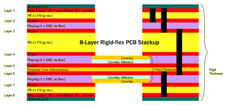
1Layer (Top rigid layer): Houses Signal traces and parts.
2Layer (Top rigid layer): Serves as the ground plane.
3Layer (Internal rigid layer): Contains signal pathways and component elements.
4Layer (Internal rigid layer): Functions as the power plane.
5Layer (Flex layer): Comprises polyimide or analogous flexible base materials.
6Layer (Flex layer): Using polyimide or likened flexible substrates.
7Layer (Internal rigid layer): Entails signal traces and integral components.
8Layer (Bottom rigid layer): Accommodates signal transmission traces and relevant components.
This stack-up provides a good balance between signal integrity, power distribution, and flexibility. The internal rigid layers typically consist of power and ground planes to provide solid power distribution and reduce noise. The signal layers are distributed between the internal rigid layers and the outer rigid layers.
The flexible layers, namely Layer 5 and Layer 6, are crafted from polyimide or comparable flexible substances, permitting the PCB to achieve a degree of deflection and flexibility without compromising its structural integrity. These layers usually possess less thickness compared to the rigid ones, thereby promoting flexibility.
Crucially, this serves as just one instance of an 8-layer rigid-flex PCB stack-up, and the particular demands of your design might call for a distinct stackup arrangement. It’s advisable to initiate consultation with your PCB fabricator and take into account their capabilities and directions to ascertain the most suitable stackup for your exclusive requirements.
Design Considerations on 8-Layer Rigid-flex PCB Boards
Designing an 8-layer rigid-flex PCB (Printed Circuit Board) requires careful consideration of various factors to ensure the board’s functionality, reliability and manufacturability.
Layer stack-up:
Determine the layer stackup configuration based on the specific requirements of your design. Consider the number and arrangement of signal layers, power and ground planes, and flex layers. Properly distributing power and ground planes is crucial for signal integrity and controlled impedance.
Material selection:
Choose appropriate materials for the rigid and flex portions of the PCB. The rigid sections typically use FR-4 or similar materials, while flexible areas require polyimide or similar flexible substrates. Ensure that the chosen materials have compatible thermal expansion coefficients to prevent mechanical stress during temperature variations.
Flex-to-rigid transition zones:
Pay special attention to the transition zones where the flexible and rigid sections meet. Gradual transitions, such as tapered flex areas or gradual changes in layer thickness, help minimize stress and strain on the flex materials during bending or flexing.
Bending and folding radius:
Determine the minimum bending and folding radius for the flex sections based on the chosen materials. Avoid sharp bends that could cause cracking or delamination. Consider the flexibility requirements of your design and select suitable materials and thicknesses accordingly.
Controlled impedance:
For high-speed signal integrity, ensure controlled impedance for critical signal traces. Calculate and design the trace widths, spacing, and layer configuration to achieve the desired impedance values. Impedance matching is particularly important for differential pairs and high-speed interfaces.
Signal and power integrity:
Analyze and enhance signal and power dissemination to curtail noise, crosstalk, and loss of power. Proper positioning of decoupling capacitors, power planes, along with signal pathway strategies (inclusive of length matching, protective shielding and differential routing) contribute towards sustaining signal integrity and reducing disruption.
Component placement and routing:
Plan the component placement strategically to accommodate the flexing requirements. Avoid placing rigid components near areas that experience frequent bending. Ensure adequate space for connectors and mechanical reinforcements in the transition zones.
Design for manufacturability:
Consider the capabilities and limitations of the manufacturing processes for rigid-flex PCBs. Collaborate closely with the PCB manufacturer to ensure the design aligns with their manufacturing capabilities. Pay attention to design rules, minimum feature sizes, and tolerances to enable successful fabrication and assembly.
Environmental and reliability considerations:
Evaluate the operating environments and mechanical stresses the PCB may encounter. Design the flex regions to withstand repeated bending, vibration, and temperature variations. Consider the use of stiffeners, coverlays, and adhesives to enhance the board’s durability and reliability.
Testing and inspection:
Plan for proper test points and access for testing and inspection during the manufacturing process and throughout the board’s lifecycle. Consider the challenges of testing the flexible sections and provide appropriate access points for probing and debugging.
Step-by-step Fabrication of 8-Layer Rigid-flex PCB
1. Design and Stack-up Planning: Determine the layer stack-up configuration, including the number of rigid and flex layers. Precisely select the materials for every layer, keeping in mind aspects like electrical efficiency, mechanical pliability and thermal attributes. Plan the placement of signal, power, and ground layers to achieve desired impedance control and signal integrity.
2. Material Preparation: Prepare the rigid and flexible foundational materials as per the design stipulations. Cut the rigid and flexible substrate into fitting dimensions, contemplating the end size of the PCB.
3. Surface Preparation: Clean the surface of the base materials to remove any contaminants or oxidation. Apply an adhesive or bonding material to the surface of the flex layers to facilitate bonding with the rigid layers.
4. Layer Alignment and Bonding: Align the rigid and flex layers together, ensuring proper registration and alignment of copper traces and vias. Apply heat and pressure to bond the layers together, using a lamination press or other suitable equipment. Cure the bonding material to achieve a strong and reliable bond between the layers.
5. Drilling and Plating: Drill holes for vias and through-hole components, ensuring precise alignment with the design. Plate the drilled holes with conductive material to establish electrical connections between different layers.
6. Copper Pattern Formation: Apply a layer of copper to the surface of the PCB, either through electroplating or etching processes. Define the desired copper patterns using a photolithography process, applying a photoresist and exposing it to UV light through a mask. Develop and etch the photoresist to remove unwanted copper, leaving behind the desired circuit traces.
7. Solder mask and Silkscreen: Apply a soldermask layer to protect the copper traces and define the areas for soldering. Add a silkscreen layer for component markings, part numbers, and other necessary information.
8. Surface Finish: Apply a surface finish to protect the exposed copper surfaces and facilitate soldering. Common surface finish options include HASL (Hot Air Solder Leveling), ENIG (Electroless Nickel Immersion Gold), or OSP (Organic Solderability Preservative).
9. Electrical Testing and Inspection: Perform electrical testing to verify the integrity of the circuit connections, including continuity, impedance, and isolation tests. Inspect the PCB for any defects, such as shorts, opens, or manufacturing errors.
10. Routing and Profiling: Route the PCB to separate individual boards from the panel, ensuring clean and precise cuts. Profile the edges of the PCB to remove any excess material and achieve the desired shape.
11. Final Inspection and Packaging: Conduct a final inspection to ensure the PCB meets the required quality standards. Package the finished PCB appropriately to protect them during transportation and storage.
Importance and Benefits of 8-Layer Rigid-flex PCB
8 layer rigid flex PCB provide numerous significant advantages and are extensively utilized across diverse industries. Below are some of the importance and advantages associated with 8 layer rigid flex PCB:
Space-saving and compact design: With multiple layers of rigid and flexible materials, 8-layer rigid-flex PCB allow for a more compact and space-efficient design compared to traditional rigid PCB. This factor holds paramount importance in scenarios where size and weight limitations are substantial considerations, such as in portable electronics, aerospace technology, and medical devices.
Improved Flexibility and Durability: The pliant layers in a rigid-flex PCB endow exceptional flexibility as well as bending proficiencies, permitting the PCB to adapt to intricate geometries and accommodate snug spaces. This flexibility further amplifies the durability of the PCB, bolstering its resistance against mechanical strain, oscillations, and thermal cycling.
Enhanced signal integrity: The multiple layers in an 8 layer rigid flex PCB enable better signal integrity and impedance control. By separating high-speed and sensitive signals from power and ground planes, signal integrity issues like crosstalk, noise, and electromagnetic interference (EMI) can be minimized, resulting in improved performance and reliability of the electronic system.
Reduced interconnects and assembly complexity: Compared to using separate rigid PCB connected with cables or connectors, 8-layer rigid-flex PCB eliminate the need for extra interconnects, reducing the overall assembly complexity and potential points of failure. This simplifies the manufacturing process, improves reliability, and lowers costs.
Increased design flexibility: The combination of rigid and flexible layers in an 8-layer rigid-flex PCB offers designers greater flexibility in routing and component placement. This allows for more efficient use of available space, optimized signal paths, and the ability to design complex, three-dimensional shapes that would be challenging with traditional rigid PCB.
Cost savings: While the initial manufacturing cost of 8-layer rigid-flex PCB may be higher compared to standard rigid PCB, the overall cost savings can be significant. The elimination of connectors, cables, and interconnects reduces material costs, assembly time, and potential points of failure, consecutively elevating reliability and diminishing long-term maintenance and repair costs.
Application versatility: The 8 layer rigid flex PCB are a preferred choice across a diverse array of industries and technologies. automotive, aerospace, medical devices, telecommunications and more. They are suitable for applications that require a combination of flexibility, durability, compactness and high-performance electronics.
Overall, 8-layer rigid-flex PCB offer a compelling solution for complex electronic systems, providing numerous benefits such as space-saving design, improved flexibility, enhanced signal integrity, reduced assembly complexity, increased design flexibility, cost savings, and application versatility.
In Conclusion
8 layer rigid flex PCB circuit boards offer a versatile and reliable solution for complex electronic designs. With their ability to combine rigid and flexible sections, these boards enable the creation of compact and lightweight devices while maintaining excellent electrical performance. From aerospace and healthcare to automotive, and consumer electronics, 8 layer rigid flex PCB have ingrained their utility broadly. As technology continues to advance, we can expect further innovations in the field of rigid flex PCB, opening up new possibilities for the development of advanced electronic devices.


