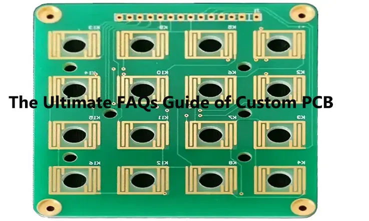
Printed Circuit Boards (PCBs) are a fundamental building block of electronic devices, providing a foundation for the interconnection and control of electronic components. Custom PCBs, also known as bespoke PCBs, are specifically designed to meet the precise requirements of an electronic device, such as size, functionality, and performance.
If you are considering importing custom PCBs, it is essential to familiarize yourself with the intricacies of this process. In this comprehensive guide, you will find detailed information about custom PCBs, including material selection, fabrication techniques, component mounting, hole drilling, and assembly procedures.
By perusing this guide, you will gain an in-depth understanding of custom PCBs, enabling you to make informed decisions about their design, manufacture, and implementation. Whether you are a seasoned professional or a newcomer to the field of electronics, this guide is an indispensable resource for achieving success in custom PCB development.
What is a Custom Printed Circuit Board ?
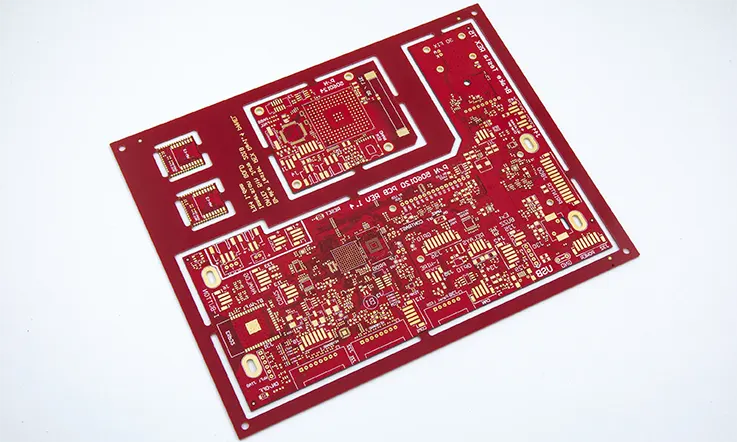
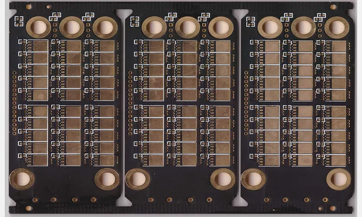
A Custom Printed Circuit Board (PCB) is a circuit board that is designed and fabricated to meet specific requirements of an electronic device. It is tailored to the needs of the device and is not a standard, off-the-shelf product. Custom PCBs can be designed for both simple and complex electronic systems, and they offer numerous advantages over traditional, off-the-shelf PCBs.
The process of designing a custom PCB involves understanding the specific requirements of the device, choosing the right software, capturing the schematic, designing the physical layout of the PCB, and running design rule checks. Once the design is complete, the custom PCB is fabricated using a manufacturing process that involves printing the design onto a substrate, etching the copper traces, drilling holes, and adding a solder mask and silkscreen layer.
How Many Types of Custom PCB ?
There are several types of custom PCBs (Printed Circuit Boards) that can be designed and manufactured to meet specific requirements. Some of the most common types of custom PCBs include:
Single-layer PCBs: These PCBs have a single layer of conductive material on one side of the board.
Double-layer PCBs: These PCBs have conductive material on both sides of the board, with vias connecting the two layers.
Multilayer PCBs: These PCBs have multiple layers of conductive material separated by insulating layers.
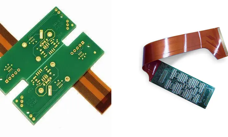
Flexible PCBs: These PCBs are made from flexible materials that can bend and conform to different shapes and sizes.
Rigid-Flex PCBs: These PCBs combine the advantages of rigid and flexible PCBs, with both rigid and flexible sections on the same board.
High-frequency PCBs: These PCBs are designed to operate at high frequencies and may use specialized materials and construction techniques.
High-density interconnect (HDI) PCBs: These PCBs use advanced manufacturing techniques to increase the density of components on the board.
The type of custom PCB that is best for a specific application will depend on the requirements of the project, such as the size and complexity of the circuit, the operating environment, and the performance specifications.
Benefits of Using Custom PCBs
The importance of custom PCBs lies in their ability to meet specific requirements of an electronic device and offer numerous advantages over traditional, off-the-shelf PCBs. The following are some of the key benefits of using custom PCBs:
Optimized performance
Custom PCBs can be designed to meet specific performance requirements, such as high-speed signaling, low noise, and low power consumption. Standard PCBs are designed to meet general requirements and may not be optimized for specific applications.
Space-saving
Custom PCBs can be designed to fit within the available space of the device, reducing the overall size of the device. This is particularly important for portable devices such as smartphones and tablets.
Cost-effective
Custom PCBs can be designed to reduce the number of components required, reducing the overall cost of the device. This is particularly important for high-volume production runs.
Improved reliability
Custom PCBs can be designed to improve the reliability of the device by reducing the risk of signal interference and noise. This is particularly important for critical applications such as medical devices and aerospace systems.
Faster time-to-market
Custom PCBs can be designed and fabricated more quickly than traditional, off-the-shelf PCBs. This enables designers to bring their products to market faster and stay ahead of the competition.
Overall, custom PCBs are an essential element in the design and development of electronic devices. They offer numerous advantages over traditional, off-the-shelf PCBs and enable designers to create products that meet specific requirements and perform optimally in their intended applications.
Which are the Disadvantages of Custom PCB ?
While custom PCBs offer many benefits, there are also some potential disadvantages to consider. Here are a few possible drawbacks of custom PCBs:
Higher cost: Custom PCBs are often more expensive to produce than standard off-the-shelf PCBs due to the additional design and manufacturing time required.
Longer lead time: Because custom PCBs require additional design and manufacturing time, they may take longer to produce than standard PCBs. This can be a disadvantage if there are tight deadlines for a project.
Higher risk of errors: Custom PCBs are more prone to errors than standard PCBs, as they are designed from scratch and may require more testing and refinement to ensure they work properly.
Limited availability: Custom PCBs may not be available from all PCB manufacturers, which can limit the options available to a designer.
Design complexity: Custom PCBs can be more complex to design, as they may require additional components or specialized features that are not available on standard PCBs.
Overall, while custom PCBs can be a great option for certain projects, it’s important to weigh the potential disadvantages against the benefits to determine whether they are the right choice for a particular application.
How to Design a Custom PCB ?
Designing a custom PCB involves several steps and requires a good understanding of the requirements of the electronic device. The following are the key steps in designing a custom PCB:
Understanding the design requirements
Before starting the design process, it is essential to understand the specific requirements of the electronic device. This includes determining the size and shape of the PCB, the number and type of components, the power requirements, and the desired performance characteristics.
Choosing the right software
There are several software tools available for designing custom PCBs, such as Eagle PCB, Altium Designer, and KiCAD. The choice of software depends on the complexity of the design and the designer’s familiarity with the software.
Schematic capture
The schematic capture is the initial step in designing a custom PCB. It involves drawing the electrical circuit using symbols to represent electronic components and connecting them through wires.
PCB layout
Once the schematic is complete, the next step is to design the physical layout of the PCB. This involves placing the components on the PCB and routing the connections between them.
Design rule checks
Before finalizing the design, it is essential to run design rule checks to ensure that the design meets the required specifications. These checks include verifying the spacing between components, the clearance between traces, and the minimum drill size.
By following these steps, a custom PCB designer can create a design that meets the requirements of the electronic device and ensures optimal performance.
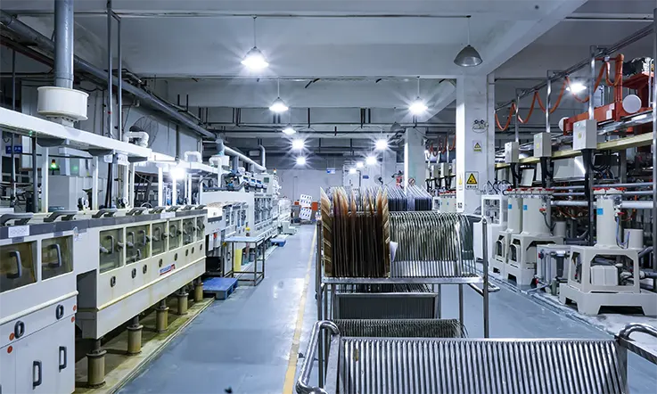
Custom PCB Fabrication Step
Custom PCB fabrication is the process of creating a printed circuit board (PCB) that is designed to meet specific requirements for a particular project or application. This process involves several steps, including designing the PCB layout, selecting the appropriate materials, and using specialized equipment to manufacture the board.
Here are some of the key steps involved in custom PCB fabrication:
1. Designing the PCB layout: The first step is to create a design for the PCB that meets the specific requirements of the project. This involves using PCB design software to create a schematic diagram of the circuit, which is then used to create the physical layout of the board.
2. Selecting the appropriate materials: The materials used in the fabrication process will depend on the specifications of the project. This may include selecting the appropriate substrate material, copper thickness, solder mask color, and other factors.
3. Creating the PCB artwork: Once the layout and materials have been determined, the next step is to create the artwork that will be used to manufacture the PCB. This involves using specialized software to create a file that contains all of the information needed to create the board.
4. Printing the artwork: The PCB artwork is then printed onto a special film that is used to create the PCB. This process is typically done using a specialized printer that is capable of producing high-quality images with fine details.
5. Manufacturing the board: Once the artwork has been printed, the PCB is manufactured using a process called etching. This involves using chemicals to remove the copper from the board in areas that are not part of the circuit. The board is then drilled and plated to create the necessary connections between components.
6. Quality control: After the board has been manufactured, it is inspected to ensure that it meets the required specifications. This may involve using specialized testing equipment to check for defects or errors in the circuit.
To sum up, custom PCB fabrication is a complex process that requires specialized knowledge and equipment. However, it can be an effective way to create high-quality PCBs that are tailored to meet the specific needs of a particular project or application.
Which are the Main Materials Used in Custom PCB ?
There are several materials commonly used in the fabrication of custom PCBs, including:
Substrate materials: The substrate material is the base layer of the PCB and provides mechanical support for the circuitry. Common substrate materials include FR-4 (a type of fiberglass-reinforced epoxy), aluminum, and ceramic.
Copper foil: Copper foil is used to create the conductive pathways on the PCB. Copper foil is available in various thicknesses, and the choice of thickness will depend on the specific requirements of the project.
Solder mask: Solder mask is a protective layer that is applied over the copper traces to prevent solder from flowing where it’s not intended during assembly. The color of the solder mask is typically green, but other colors are also available.
Silkscreen: Silkscreen is a layer of ink that is applied over the solder mask to provide labeling and identification for the components on the PCB.
Surface finish: The surface finish is a coating that is applied to the exposed copper to protect it from oxidation and to improve the solderability of the PCB. Common surface finishes include HASL (hot air solder leveling), ENIG (electroless nickel immersion gold), and OSP (organic solderability preservatives).
Adhesive: Adhesive is used to bond the layers of the PCB together. The type of adhesive used will depend on the specific substrate material and the manufacturing process.
All in all, the choice of materials for a custom PCB will depend on the specific requirements of the project, including the desired performance characteristics, cost considerations, and manufacturing constraints. By carefully selecting the appropriate materials and manufacturing processes, it is possible to create a custom PCB that meets the required specifications and performs as expected.
What is DFM Checks in Custom PCB Fabrication ?
Design for Manufacturability (DFM) checks are a set of design guidelines used in the fabrication of custom printed circuit boards (PCBs) to ensure that the design is optimized for efficient and cost-effective manufacturing. These checks are performed by the PCB manufacturer to identify and address any design issues that could impact the quality or reliability of the finished product.
The DFM checks can include a review of the layout, component placement, routing, and other design elements to ensure that they are compatible with the manufacturing process and can be produced efficiently and accurately. By performing DFM checks, the manufacturer can help to ensure that the final product meets the intended specifications and is delivered on time and within budget.
Why is Drill Hole Size Tolerance Important During Fabrication of Custom PCB?
Drill hole size tolerance is an important consideration during the fabrication of custom PCBs because it can impact the performance and reliability of the finished product. The drill holes in a PCB are used to create connections between different layers of the board, and if the holes are not drilled to the correct size, it can result in a poor connection or even a complete failure of the PCB.
For example, if the drill holes are too small, it can make it difficult to insert the necessary components or to solder the connections, which can result in a weak or unreliable connection. On the other hand, if the drill holes are too large, it can lead to a loose or unstable connection, which can also impact the performance and reliability of the PCB.
To ensure that the drill holes are drilled to the correct size, it is important to specify the appropriate tolerance during the design phase of the PCB. This tolerance should take into account the specific requirements of the project and the capabilities of the manufacturing process, and should be verified during the quality control process to ensure that the finished product meets the required specifications.
Overall, drill hole size tolerance is an important consideration during the fabrication of custom PCBs, as it can impact the performance and reliability of the finished product. By specifying the appropriate tolerance and verifying it during the quality control process, it is possible to ensure that the finished product meets the required specifications and performs as expected.
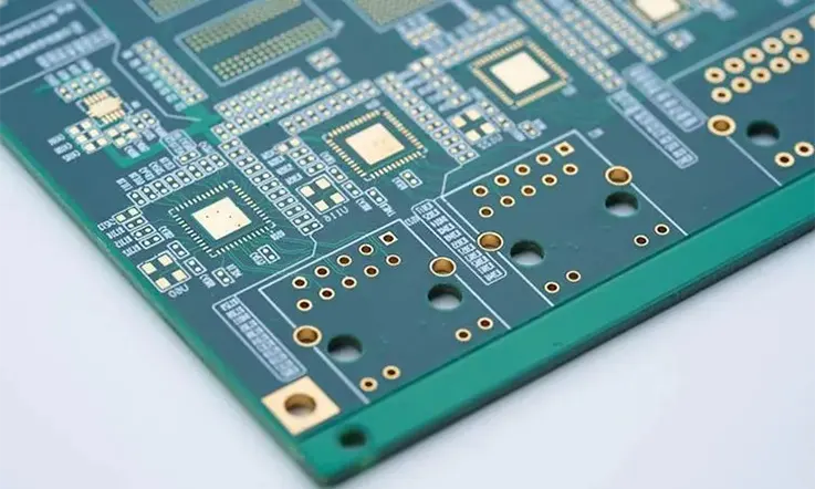
Which are the Different Types of Vias Used in Custom PCB ?
Vias are small holes that are drilled into a PCB and used to create connections between different layers of the board. There are several different types of vias commonly used in custom PCBs, including:
Through-hole vias: Through-hole vias are the most common type of via and are used to create connections between the top and bottom layers of the PCB. These vias are drilled all the way through the PCB and are plated with copper to create a conductive pathway.
Blind vias: Blind vias are drilled from the surface of the PCB down to an inner layer, but do not go all the way through the board. These vias are used to create connections between the outer layers and one or more inner layers of the PCB.
Buried vias: Buried vias are drilled between two inner layers of the PCB and do not extend to the outer layers. These vias are used to create connections between inner layers of the board without affecting the outer layers.
Microvias: Microvias are very small vias that are typically less than 0.15mm in diameter. These vias are used in high-density designs where space is limited.
Stacked vias: Stacked vias are multiple through-hole vias that are stacked on top of each other. These vias are used to create connections between multiple layers of the PCB.
Via-in-pad: Via-in-pad is a design technique where a via is placed directly under a component pad. This technique can help to save space and reduce signal noise.
Therefore, the choice of via type will depend on the specific requirements of the project, including the desired performance characteristics, cost considerations, and manufacturing constraints. By carefully selecting the appropriate via type and design, it is possible to create a custom PCB that meets the required specifications and performs as expected.
Do You Need a PCB Prototype when Developing Custom PCB ?
In most cases, it is a good idea to create a PCB prototype when developing a custom PCB. A prototype allows you to test and refine the design before moving on to full-scale production, which can help to identify and address any issues or errors in the design before they become bigger problems.
Creating a prototype can also help you to evaluate the performance of the PCB in real-world conditions and make any necessary adjustments to the design. This can be especially important in applications where reliability and accuracy are critical.
There are several methods for creating a PCB prototype, including using a breadboard or perfboard to create a simple prototype, or using a specialized PCB prototyping service to create a more advanced prototype.
Overall, while it may be possible to skip the prototype stage in some cases, it is generally recommended to create a prototype when developing a custom PCB to help ensure that the final product meets the intended specifications and performs as expected.
How Do You Assemble Custom PCB ?
Custom PCBs can be assembled using a variety of different methods, depending on the complexity of the design and the specific requirements of the project. Here are some of the most common methods for assembling custom PCBs:
Surface Mount Technology (SMT): SMT is a popular method for assembling custom PCBs, especially those with small components and high-density designs. SMT involves placing components directly onto the surface of the PCB and then soldering them into place using a reflow oven.
Through-Hole Technology (THT): THT involves inserting components through holes in the PCB and then soldering them onto the opposite side of the board. THT is commonly used for larger components and connectors that cannot be surface-mounted.
Mixed Technology: Mixed technology involves using both SMT and THT components on the same PCB. This method is often used when a design requires a combination of small and large components.
Automated Assembly: Automated assembly involves using robotic equipment to place and solder components onto the PCB. This method is often used for large-scale production runs, as it can help to improve efficiency and reduce costs.
Hand Assembly: Hand assembly involves manually placing and soldering components onto the PCB. This method is often used for small-scale or prototype production runs, as it can be more time-consuming and labor-intensive than automated assembly.
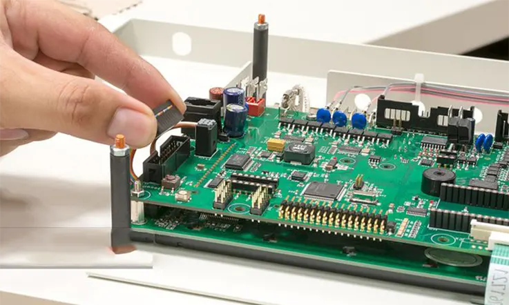
Overall, the method of assembling a custom PCB will depend on the specific requirements of the project, including the complexity of the design, the size of the components, and the volume of the production run. By carefully selecting the appropriate assembly method, it is possible to create a custom PCB that meets the required specifications and performs as expected.
When Should You Choose Custom PCBs ?
Custom PCBs are a good choice in a variety of situations, including:
1. When the project requires specific features or functionality that is not available on a standard PCB: Custom PCBs can be designed to include specialized features or functionality that may not be available on a standard PCB.
2. When the project requires a specific form factor or size: Custom PCBs can be designed to fit specific form factors or sizes, which can be important in applications where space is limited.
3. When the project requires a high level of precision or accuracy: Custom PCBs can be designed to very precise specifications, which can be important in applications where accuracy is critical.
4. When the project requires a high level of reliability or durability: Custom PCBs can be designed with materials and manufacturing processes that are optimized for reliability and durability, which can be important in applications where the PCB will be subjected to harsh environments or rough handling.
5. When the project requires a high level of customization or personalization: Custom PCBs can be designed to include personalized branding, logos, or other custom features that can help the project stand out.
As a result, custom PCBs are a good choice when the project requires specific features, functionality, form factors, or levels of precision or reliability that are not available on a standard PCB. It’s important to weigh the potential benefits of custom PCBs against the potential drawbacks, such as higher cost and longer lead times, to determine whether they are the right choice for a particular application.
Why Conformal Coating is Your Custom PCB Option?
Conformal Coating, also known as three-proof adhesive, insulating adhesive, moisture-proof agent, moisture-proof oil, protective paint, or protective paint, is a specialized coating that provides protection to electronic components. While it is commonly associated with preventing moisture, mold, and salt spray (the “three anti” function), its protective capabilities extend far beyond that.
In addition to its moisture-resistant properties, Conformal Coating provides protection against dust, friction, shock, high temperatures, and chemical environments. It also helps prevent PCB circuit board failure, enhances insulation strength, and extends the life of the circuit board.
When applied, Conformal Coating creates a dense protective film on the surface of the PCB, effectively shielding the circuit from environmental erosion. As a result, it is an indispensable component in ensuring the longevity and reliability of electronic devices.
How to Choose the Reliable Custom PCB Manufacturer ?
Choosing a reliable custom PCB manufacturer is an important step in ensuring the quality and performance of your PCBs. Here are some factors to consider when choosing a custom PCB manufacturer:
1. Experience and Reputation: Look for a manufacturer with a proven track record of producing high-quality PCBs. Check their website for customer reviews and testimonials, and see if they have experience in manufacturing PCBs for your specific industry or application.
2. Quality Control: Ask about the manufacturer’s quality control processes and certifications. Look for a manufacturer that uses high-quality materials, performs rigorous testing, and has certifications such as ISO 9001 or UL.
3. Technical Expertise: Ensure that the manufacturer has the technical expertise to handle your project’s requirements. Ask about their experience with the specific materials, components, and manufacturing processes needed for your project.
4. Customer Service: Look for a manufacturer that provides excellent customer service, including clear communication, fast response times, and a willingness to work with you to resolve any issues that may arise.
5. Pricing and Lead Times: Compare pricing and lead times from multiple manufacturers to ensure that you are getting a competitive price and a realistic production timeline.
6. Location and Shipping: Consider the location of the manufacturer and their shipping options. A manufacturer located closer to your facility may offer faster shipping times and lower shipping costs.
By considering these factors, you can choose a reliable custom PCB manufacturer that can provide high-quality, cost-effective PCBs for your project.
Why Choose Jarnistech Custom PCBs ?
For more than two decades, we have been a leading manufacturer of custom PCBs, catering to diverse industries. Our custom PCBs are designed with cutting-edge features that can elevate the performance of your applications significantly.
At JarnisTech, we prioritize delivering custom PCBs of the highest quality. Our team adheres to industry best practices to ensure that the PCBs we manufacture are tailored to meet your specific requirements and fully functional.
We understand the importance of precision and reliability in PCB manufacturing, and we employ the latest techniques and technologies to guarantee that your boards will fit your applications perfectly. With our custom PCBs, you can rest assured that you are getting a top-of-the-range product that will enhance the quality and performance of your applications.
FAQ Section of Custom PCBs
Here are some common questions and answers related to custom PCBs:
Q: How much does a custom PCB cost?
A: The cost of a custom PCB will depend on several factors, including the complexity of the design, the materials used, and the volume of the order. Generally, custom PCBs are more expensive than standard off-the-shelf PCBs due to the additional design and manufacturing time required.
Q: How long does it take to make a custom PCB?
A: The lead time for a custom PCB will depend on several factors, including the complexity of the design, the materials used, and the volume of the order. Generally, custom PCBs take longer to produce than standard off-the-shelf PCBs due to the additional design and manufacturing time required.
Q: What are some common mistakes to avoid when designing a custom PCB?
A: Some common mistakes to avoid when designing a custom PCB include not leaving enough space between components, not following design rules for the specific PCB manufacturer being used, and not properly testing the design before manufacturing.
Q: What industries and fields use custom PCBs?
A: Custom PCBs are used in a wide range of industries and fields, including aerospace, automotive, medical, telecommunications, and consumer electronics, among others.
Q: What software is used to design custom PCBs?
A: There are many software tools available for designing custom PCBs, including Altium Designer, Eagle PCB, KiCAD, and others.
Q: What materials are commonly used in custom PCB fabrication?
A: Common materials used in custom PCB fabrication include FR-4, aluminum, ceramic, and flexible materials such as polyimide.
Q: Can you Reverse Engineer Custom PCB?
A: At time the schematic of printed circuit board can be lacking.
In such situations, it is possible to reverse engineer a custom PCB, but it can be a difficult and time-consuming process. Reverse engineering involves analyzing the design of the PCB to determine its functionality and how it was created. This can involve using specialized equipment to examine the PCB under a microscope, analyzing the layout and component placement, and tracing the circuitry to determine its function.
Q: What is the difference between a through-hole and surface-mount component?
A: Through-hole components have leads that are inserted through holes in the PCB and soldered on the other side, while surface-mount components are soldered directly to the surface of the PCB. Surface-mount components are generally smaller and more compact than through-hole components.
These are just a few examples of common questions related to custom PCBs. If you have specific questions related to your project or application, it’s best to consult with a JarnisTech PCB manufacturer or engineer to get more personalized advice and guidance.
Conclusion
Custom PCBs are an essential component in modern electronics design and manufacturing. They enable precise control and measurement of electrical signals, allow for compact and high-performance circuitry, and can be tailored to specific product requirements. Custom PCBs are used in a wide range of industries and fields, including consumer electronics, medical devices, aerospace and defense, industrial automation, automotive, and Internet of Things (IoT) devices.
With the ability to design and manufacture PCBs to specific requirements, custom PCBs offer endless possibilities for innovation and product development. Whether you are working on a new consumer product, medical device, or industrial automation system, custom PCBs can be an invaluable tool for bringing your ideas to life.