
The trajectory of electronic design is shifting from static, rigid structures toward dynamic and conformable applications. This evolution is enabled by Flexible Printed Circuits (FPCs), which allow circuitry to bend, fold, and integrate within non-traditional product shapes. The performance and reliability of any FPC, however, originate from its constituent material: the Flexible Copper Clad Laminate (FCCL).
A thorough grasp of FCCL properties directly affects every stage of a flexible circuit project, from initial concept to final assembly. The selection of an appropriate FCCL grade influences not only the circuit’s electrical behavior but also determines its mechanical endurance and the operational integrity of the end product.
This guide dissects the composition and fabrication details of FCCL. The objective is to provide a clear view of how material selection cascades through to the final application’s performance. To achieve this, we will examine the following areas in detail:
1.Core Components: An analysis of polyimide (PI) versus polyester (PET) base films, combined with different copper foil types and adhesive systems.
2.Material Categories and Selection: A comparison of adhesiveless and adhesive-based FCCL, outlining their respective technical merits and typical use cases.
3.Performance Metrics: Guidance on interpreting data points such as dielectric constant, peel strength, and dimensional stability to align with specific design requirements.
The Anatomy of Flexible Copper Clad Laminate (FCCL)
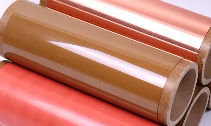
A sheet of Flexible Copper Clad Laminate is a precisely engineered composite material. Each layer within its structure has a distinct function that collectively determines the laminate’s electrical and mechanical characteristics. Understanding these individual components is foundational to proper material selection and successful flexible circuit design.
Dielectric Substrate Film
This non-conductive film provides the structural foundation and electrical insulation for the circuit. The choice of substrate material directly affects the laminate’s thermal stability, chemical resistance, and overall durability.
●Polyimide (PI): Offers superior thermal performance and high dimensional stability, making it suitable for applications requiring soldering or exposure to elevated temperatures.
●Polyester (PET): Provides a cost-effective alternative with good flexibility and adequate electrical properties for less demanding consumer electronics.
Conductive Copper Foil
This layer of high-purity copper serves as the conductive medium from which circuit traces are etched. The type and properties of the copper foil influence the circuit’s current-carrying capacity, signal integrity, and endurance under repeated flexing.
●Rolled-Annealed (RA) Copper: Characterized by a smooth surface and horizontally-oriented grain structure, offering maximum flexibility and fatigue resistance for dynamic applications.
●Electro-Deposited (ED) Copper: Features a vertical grain structure and rougher surface profile. It is a standard choice for static or less demanding flexible applications.
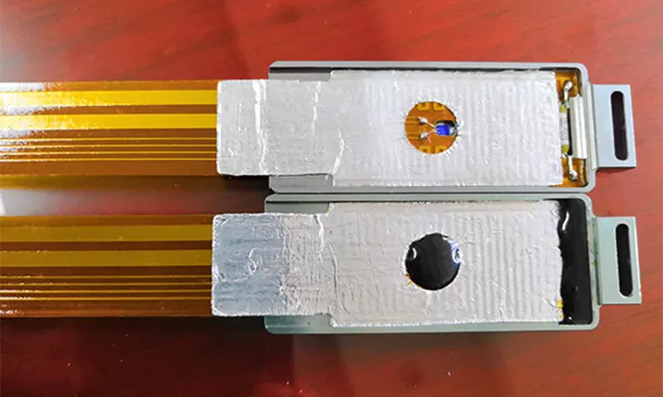
Adhesive System
In many FCCL constructions, a specialized adhesive is used to bond the copper foil to the dielectric substrate. This bonding layer is an engineered polymer system that contributes to the laminate’s overall peel strength, thermal conductivity, and chemical resistance. The presence and type of adhesive can alter the final electrical performance, particularly in high-frequency circuits. Adhesiveless constructions, where copper is deposited directly onto the film, offer an alternative with a thinner profile and enhanced thermal properties.
The specific combination of these three layers defines an FCCL’s complete performance profile and its suitability for any given electronic application.
FCCL Types and Classifications
Flexible Copper Clad Laminates are available in numerous variations, each engineered for specific performance requirements. Materials are typically categorized by their layer count, composition, substrate chemistry, and specialized properties. A methodical selection based on these classifications is a preliminary step toward a successful design and assembly process.
Classification by Layer Structure
This category describes the number of conductive copper layers in the laminate.
1.Single-Sided FCCL A single copper layer is bonded to one side of a dielectric film. This is the most straightforward construction, offering excellent flexibility and cost-effectiveness.
●Applications: Membrane switches, display interconnects, simple sensor circuits, and antennas.
2.Double-Sided FCCL Features a copper layer on both sides of a central dielectric film. This configuration permits more complex circuit layouts by using plated through-holes (vias) to connect the two sides.
●Applications: Compact cameras, automotive control modules, disk drives, and devices requiring a higher density of components.
3.Multi-Layer Flexible Laminates These are constructed by bonding several single or double-sided flexible circuits together with insulating adhesive layers. This method achieves the highest possible circuit density within a compact, flexible volume.
●Applications: Aerospace avionics, medical imaging systems, military hardware, and other high-density interconnect solutions.
Classification by Material Composition
This describes how the copper and dielectric layers are joined.
●3L-FCCL (Adhesive-Based) This construction uses a layer of adhesive to bond the copper foil to the dielectric film (Copper / Adhesive / Film). It is a widely used and economical option for many general-purpose applications. However, the adhesive layer can limit thermal performance and the ability to etch very fine circuit features.
●2L-FCCL (Adhesiveless) This two-layer construction bonds the copper directly to the dielectric film, typically through casting or sputtering methods. The elimination of the adhesive layer results in a thinner profile, improved heat resistance, and superior dimensional stability. This stability facilitates the fabrication of circuits with very fine lines and spaces.
Classification by Substrate Polymer Chemistry
The choice of dielectric film governs the laminate’s thermal, mechanical, and electrical behavior.
●Polyimide (PI) FCCL The most widely used substrate, offering a well-rounded performance profile that includes high-temperature resistance and robust mechanical durability.
●Polyester (PET) FCCL A lower-cost material with good flexibility but limited resistance to high temperatures, making it suitable for disposable or single-use consumer electronics.
●Liquid Crystal Polymer (LCP) FCCL A high-performance substrate with exceptionally low signal loss at high frequencies and very low moisture absorption. Its properties make it a preferred choice for 5G, mmWave, and other high-speed digital and RF applications.
●Modified Polyimide (MPI) FCCL An advanced form of polyimide engineered to offer lower signal loss than standard PI, serving as a performance bridge between standard PI and more specialized substrates like LCP.
Classification by Specialized Properties
These materials are formulated to meet specific regulatory, thermal, or optical needs.
1.Halogen-Free FCCL Formulated without bromine or chlorine compounds to comply with environmental standards like RoHS. These materials reduce the emission of toxic smoke in case of fire.
2.High-Tg FCCL A type of 3L-FCCL that uses a high-performance adhesive with an elevated glass transition temperature (Tg). This improves the laminate’s ability to remain stable at higher operational or assembly temperatures.
3.White or Black FCCL These laminates are designed for optical applications.
●White FCCL: Features a highly reflective surface to maximize light output in LED lighting strips and backlights.
●Black FCCL: Utilizes a dark, non-reflective surface to absorb stray light and improve contrast in camera modules and optical sensors.
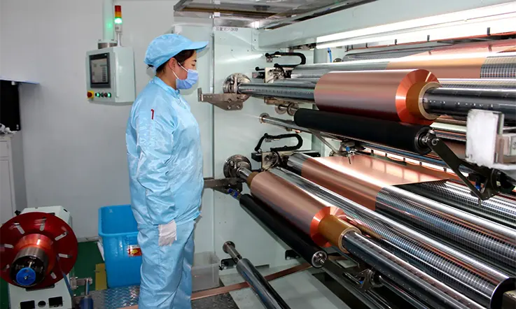
The Fabrication of Flexible Copper Clad Laminates
The fabrication of FCCL is a multi-stage technical process where control at each step directly influences the final material’s performance characteristics. The methods employed determine the laminate’s thermal properties, dimensional stability, and suitability for subsequent circuit manufacturing and assembly operations.
Substrate Film Preparation
The process commences with the base dielectric film, which must be prepared to ensure proper layer adhesion.
●Surface Cleaning: The film undergoes a thorough cleaning procedure to remove any particulate or chemical residues from its surface.
●Surface Treatment: A treatment, often involving plasma exposure, is applied to alter the film’s surface topography and energy. This modification promotes a robust bond with the subsequent copper layer.
Adhesive Application (3L-FCCL Only)
For three-layer (3L) constructions, an adhesive system is applied before the copper bonding stage. A liquid polymer adhesive, typically acrylic or epoxy-based, is coated onto the prepared film with a highly uniform thickness. The coated film is then passed through a series of ovens to partially cure the adhesive, preparing it for the lamination cycle.
Copper Layer Bonding
This is the stage where the conductive copper is joined to the dielectric film. The specific method used is a defining difference between laminate types.
●3L Lamination: A sheet of copper foil is laminated to the adhesive-coated dielectric film. This is done using large presses that apply immense pressure and elevated temperatures to activate the adhesive and permanently bond the three layers together.
●2L Direct Deposition: For adhesiveless laminates, the copper is applied directly to the film. This is achieved through more advanced techniques like solution casting the polyimide onto copper foil, or sputtering a thin layer of copper directly onto the film surface in a vacuum environment. These methods yield laminates with higher thermal endurance.
Curing and Thermal Stabilization
The newly formed laminate roll undergoes a final, extended heating cycle in a curing oven. This stage is necessary to fully cross-link the polymer chains in the dielectric and adhesive (if present). This process locks in the material’s final mechanical properties, such as tensile strength and dimensional stability at various temperatures.
Finishing, Inspection, and Packaging
The final stage involves preparing the bulk laminate for shipment and subsequent circuit fabrication.
●Inspection: The finished rolls are subjected to automated and visual inspection to detect any surface imperfections or variations in thickness.
●Slitting and Cutting: The large rolls are slit into narrower widths or cut into specific sheet sizes based on application requirements.
●Packaging: The finished FCCL material is sealed in protective, moisture-proof packaging to prevent contamination and preserve its properties during transit and storage.
Performance Metrics for FCCL Selection
The performance of a Flexible Copper Clad Laminate is defined by a set of quantifiable specifications. These metrics describe a material’s behavior under thermal, mechanical, and electrical loads. An understanding of these data points allows for informed material selection to meet the demands of both the end application and the fabrication process.
Thermal Properties
| Thermal Property | Typical Value Range | Units | Application Relevance |
| Glass Transition Temp (Tg) | 180–400 | °C | Stability during reflow/soldering; prevents delamination |
| Coefficient of Thermal Expansion (CTE) | 10–60 | ppm/°C | Minimizes stress mismatch with copper; improves solder joint reliability |
| Thermal Conductivity | 0.1–0.5 | W/m·K | Heat dissipation from active components |
1.Glass Transition Temperature (Tg) The temperature at which the material’s polymer structure transitions from a rigid to a softened, rubbery state.
●Application Relevance: A higher Tg indicates better material stability during high-temperature assembly processes like soldering, reducing the risk of delamination or damage.
2.Coefficient of Thermal Expansion (CTE) A measurement of the fractional change in a material’s size in response to a change in temperature. It is typically measured in parts per million per degree Celsius (ppm/°C).
●Application Relevance: A low CTE that closely matches that of copper minimizes mechanical stress on solder joints and plated through-holes during thermal cycling, enhancing long-term reliability.
3.Thermal Conductivity A measure of a material’s ability to transfer heat.
●Application Relevance: Although most dielectric films are thermal insulators, higher thermal conductivity helps dissipate heat from active components, potentially improving device performance and lifespan.
Dimensional Stability
This metric quantifies the percentage of change in a material’s dimensions after exposure to the temperature and chemical stresses of the circuit fabrication process.
●Application Relevance: High dimensional stability is a requirement for manufacturing high-density and multi-layer flexible circuits, as it ensures accurate layer-to-layer registration and the precise formation of fine-pitch features.
Electrical Characteristics
| Electrical Property | Typical Value | Units | Application Relevance |
| Dielectric Constant (Dk) | 2.9–3.5 (at 1 GHz) | — | Affects signal speed and impedance control |
| Dissipation Factor (Df) | 0.001–0.01 | — | Lower values reduce signal loss in RF and high-speed applications |
| Dielectric Strength | 100–300 | kV/mm | Prevents electrical breakdown between conductive layers |
1.Dielectric Constant (Dk or ϵr) A measure of a material’s ability to store electrical energy in an electric field.
●Application Relevance: For high-speed applications, substrates with a lower Dk are preferred, as they permit faster signal propagation and help maintain signal integrity.
2.Dissipation Factor (Df or tanδ) A measure of the electrical energy absorbed and lost as heat within the dielectric material when subjected to an alternating electric field.
●Application Relevance: A low Df is specified for high-frequency circuits (e.g., RF, microwave, 5G) to minimize signal attenuation and preserve signal strength over distance.
3.Dielectric Strength The maximum voltage gradient that the dielectric material can withstand without electrical breakdown or failure.
●Application Relevance: This property defines the material’s insulating capability and its capacity to prevent short circuits between conductive layers at a given operating voltage.
Mechanical Properties
| Mechanical Property | Typical Value Range | Units | Application Relevance |
| Peel Strength | ≥ 0.7–1.0 | N/mm | Ensures copper remains bonded during flexing or assembly |
| Flexural Endurance | ≥ 10,000 (dynamic cycles) | Cycles | Reliability in dynamic flex applications (e.g., laptop hinges) |
| Tensile Strength | 100–200 | MPa | Resistance to tearing or mechanical damage |
| Elongation | 10–70 | % | Indicates flexibility and ductility of the material |
1.Peel Strength The force required to separate the bonded copper foil from the dielectric substrate.
●Application Relevance: High peel strength indicates a robust bond between layers, ensuring that circuit traces and component pads do not lift during assembly, rework, or under physical stress.
2.Flexural Endurance A measure of a material’s ability to withstand repeated bending or folding cycles before conductor failure.
●Application Relevance: This is a primary specification for dynamic applications where the circuit will be constantly flexed, such as in hinges for laptops, robotics, or printers.
3.Tensile Strength and Elongation Tensile strength is the maximum stress a material can handle while being pulled apart. Elongation measures how much the material can stretch before it breaks.
●Application Relevance: These metrics together describe the material’s general toughness and its ability to survive the mechanical stresses of handling and assembly without tearing or fracturing.
FCCL in Context: A Comparison with Rigid Laminates
To understand the specific applications for Flexible Copper Clad Laminate, it is useful to compare its properties against those of common rigid printed circuit board materials. This analysis clarifies the engineering trade-offs that guide material selection for any given design.
Comparison with FR-4
The most common comparison is between flexible polyimide-based FCCL and FR-4, the industry standard for rigid PCBs composed of woven fiberglass and epoxy resin. The choice between them represents a direct trade-off between mechanical flexibility and structural rigidity.
●Form Factor: FCCL is engineered for three-dimensional applications, allowing circuits to bend, fold, and conform to a product’s housing. FR-4 provides a flat, rigid plane for component mounting.
●Mechanical Durability: In applications with high vibration or mechanical shock, the pliability of FCCL allows it to absorb energy and resist conductor fatigue. Rigid FR-4 can be susceptible to solder joint failure or micro-fractures under similar stress.
●Thermal Performance: While specialized high-temperature FR-4 variants exist, standard polyimide-based FCCL generally offers a higher maximum operating temperature, a requirement for many aerospace and automotive applications.
●Processing: FR-4 fabrication is a mature and highly standardized process. Processing FCCL requires specialized handling protocols and equipment to manage thin materials and maintain dimensional control during assembly.
●Cost Profile: FR-4 is an exceptionally cost-effective substrate. The advanced polymers and specialized manufacturing processes associated with FCCL result in a higher material cost.
●Selection Rationale: FR-4 is the default substrate for countless reliable, planar electronic devices where cost is a primary driver. FCCL is specified when the design requirements for flexibility, weight reduction, or three-dimensional packaging cannot be met by a rigid solution.
Comparison with High-Frequency Rigid Laminates
This comparison addresses applications in RF, microwave, and high-speed digital systems, pitting high-performance FCCL against specialty rigid materials from suppliers like Rogers or Taconic.
●Electrical Performance: Both categories offer substrates with very low dielectric constant (Dk) and dissipation factor (Df). Electrically, a circuit on a high-performance LCP or PTFE-based FCCL can deliver similar performance to one on a rigid microwave-grade laminate.
●Application and Form: High-frequency rigid laminates are used to create planar components like patch antennas, power amplifiers, and filters. High-frequency FCCL provides the same electrical performance but liberates it from a flat plane, allowing, for example, an antenna to conform to a curved surface or a high-speed interconnect to bend within a compact module.
●Selection Rationale: The decision is rarely based on electrical performance trade-offs, but on mechanical necessity. For planar high-frequency circuits, rigid laminates are the standard. Where the circuit must bend or conform, high-performance FCCL is the designated solution.
Comparison with Insulated Metal Substrate (IMS)
IMS laminates feature a thin dielectric layer bonded to a thick metal base, typically aluminum. They are designed for a single purpose: thermal management.
●Primary Function: The function of an IMS board is to efficiently conduct heat away from high-power components. The function of an FCCL is to provide flexible interconnection.
●Physical Properties: IMS boards are inherently rigid due to their metal core. FCCL is designed for flexibility.
●Application Example (LEDs): This contrast is clear in LED lighting. IMS is used for high-power, rigid light bars and fixtures where heat dissipation is the main technical challenge. FCCL is used for flexible LED strips that can be fitted to architectural contours.
●Thermal Management: IMS offers the highest level of thermal dissipation. However, FPC designs can manage moderate heat loads through techniques like integrated copper ground planes or the use of thermal vias and stiffeners.
●Selection Rationale: The choice represents a fundamental trade-off. IMS is the specified material when efficient heat removal is the overriding design constraint. FCCL is chosen when mechanical flexibility, space, or weight are the primary design drivers.
Advanced FPC Fabrication and Assembly Processes
Converting Flexible Copper Clad Laminate into a functional circuit assembly is a sequence of technologically advanced and tightly regulated manufacturing stages. Success at each step is determined by process control, specialized equipment, and a deep understanding of how to handle flexible materials to produce a reliable final product.
High-Resolution Circuit Imaging
This stage defines the circuit pattern onto the laminate surface. Modern fabrication substitutes traditional film-based phototools with direct imaging methods for superior accuracy.
●Process: Laser Direct Imaging (LDI) systems are utilized to expose the circuit pattern directly onto the photoresist-coated FCCL.
●Benefit: LDI eliminates artwork distortion, improves layer-to-layer registration accuracy, and enables the creation of the fine lines and spaces (e.g., < 75µm) required for high-density designs.
Controlled Impedance Etching
This chemical process removes unwanted copper to form the final circuit traces. Precision is paramount to meet electrical performance specifications.
●Process: Panels are processed through conveyorized spray-etching chambers where chemical concentrations, temperatures, and spray pressures are continuously monitored.
●Benefit: This method ensures uniform trace width and profile along the entire circuit length, preventing undercutting. This level of control is a requirement for producing circuits with specific impedance values.
Automated Coverlay and Stiffener Placement
An insulating coverlay film (typically polyimide with adhesive) is applied to protect the copper circuitry.
●Process: Automated optical alignment (AOA) systems are used to position the coverlay with high precision relative to the circuit features before bonding in a vacuum lamination press.
●Benefit: AOA prevents misregistration, and vacuum lamination ensures a void-free bond. The same precision is applied to placing FR-4 or polyimide stiffeners, which provide mechanical support for components and connectors.
Surface Finish Application
A surface finish is applied to the exposed copper pads to protect them from oxidation and provide a solderable surface for component assembly. The choice of finish depends on the application and assembly requirements.
●ENIG (Electroless Nickel Immersion Gold): Offers a flat, durable surface with excellent solderability, suitable for most SMT applications.
●ENEPIG (Electrol-ess Nickel Electroless Palladium Immersion Gold): Provides enhanced protection for the nickel layer, making it a robust solution for gold wire bonding and multiple reflow cycles in more demanding environments.
Specialized SMT on Flexible Circuits
Surface Mount Technology (SMT) assembly on flexible substrates requires specific techniques to manage the pliable nature of the material.
●Process: The FPC is temporarily secured onto a rigid carrier panel. This allows the flexible circuit to be held perfectly flat and stable throughout the entire SMT process, from automated solder paste printing and component placement to the reflow soldering oven.
●Thermal Control: The reflow oven’s thermal profile—the specific temperature ramp, soak, and peak settings—is custom-developed for each assembly. This ensures the formation of reliable solder joints without subjecting the flexible laminate to excessive thermal stress.
Quality Assurance and Testing Protocols for Flexible Circuits
For applications in fields where operational reliability is a primary requirement, product quality is ensured through a systematic framework of inspection, testing, and process control. These protocols are applied at multiple stages of the fabrication cycle to verify compliance with design specifications and performance standards.
Automated Optical Inspection (AOI)
This is a non-destructive, in-process inspection method used to scan circuit patterns for defects.
●Process: After the etching stage, 100% of circuit panels are scanned by high-resolution AOI systems. The system captures a detailed image of the copper features.
●Purpose: To compare the etched circuitry against the original digital design data (Gerber/CAD). This allows for the immediate detection and flagging of any anomalies, such as shorts, opens, or variations in trace width, preventing non-conforming product from moving to the next stage.
Physical Analysis (Micro-sectioning)
This is a destructive analysis technique performed on representative coupons from production panels to verify internal construction quality.
●Process: A sample coupon is cut from the panel, mounted in an epoxy resin, and polished. This exposes a cross-sectional view of the circuit’s internal structure for microscopic examination.
●Purpose: To visually inspect the quality of plated through-holes, confirm the accuracy of layer-to-layer registration, and verify the integrity of the lamination bond between different material layers.
Electrical and Impedance Testing
This stage verifies the electrical integrity and performance of the finished circuits.
●Continuity and Isolation Testing: Every circuit undergoes automated electrical testing (“flying probe” or “bed of nails”) to confirm there are no open circuits (opens) or unintended connections between nets (shorts).
●Controlled Impedance Verification: For high-speed circuits, test coupons on the panel are measured using a Time-Domain Reflectometer (TDR). This provides a precise measurement of the characteristic impedance of circuit traces, confirming they meet the design requirements for signal integrity.
Product Reliability and Qualification Testing
This involves subjecting finished circuits to a battery of stress tests designed to simulate harsh operating conditions and verify long-term durability.
●Process: Sample circuits undergo various tests, including thermal shock (rapid temperature cycling), high-temperature/high-humidity exposure, and dynamic flexural endurance testing for a specified number of cycles.
●Purpose: To validate the robustness of the design and the manufacturing process. Passing these tests provides data-driven confidence in the product’s ability to perform reliably over its expected service life.
Component and Lot Traceability System
This is a data management system that provides a complete history for every circuit produced.
●Process: Each panel or individual circuit is assigned a unique serial number at the start of the process. This serial number is linked in a database to all relevant manufacturing data.
●Purpose: To provide full traceability from the finished unit back to the specific raw material lots (e.g., FCCL batch), machine processing parameters, operator logs, and inspection results. This system is foundational for rigorous process control and efficient root cause analysis.
Collaborative Engineering: Design for Manufacturability (DFM)
The successful fabrication of a flexible circuit begins long before any material is processed. It starts with Design for Manufacturability (DFM), a collaborative and systematic review of the circuit design data. This process is intended to align the design’s requirements with established fabrication capabilities to ensure an efficient manufacturing cycle and a reliable final product.
DFM Process Objectives
The DFM review is a data-driven analysis performed by process specialists. Its primary objectives are:
●To identify any design features that could pose a challenge during fabrication, potentially affecting yield or delivery timelines.
●To suggest specific, actionable design modifications that can enhance the circuit’s long-term mechanical and electrical reliability.
●To optimize the design for material usage and process efficiency, which helps manage overall project costs.
Core Analysis Areas for Flexible Circuits
DFM for flexible circuits concentrates on the unique mechanical aspects of a pliable substrate. Analysis includes a thorough review of the following:
●Bend Radius Verification: Confirming that all specified bend areas maintain a sufficient radius to prevent over-stressing the copper conductors during flexing.
●Trace Routing in Bend Zones: Ensuring that conductor traces run perpendicular to bends, and that vias or component pads are not located within dynamic flex areas where they would create stress points.
●Pad-to-Trace Transitions: Recommending the addition of teardrop-shaped fillets where traces join pads. This feature disperses mechanical stress at a common point of failure, enhancing the board’s durability.
●Coverlay and Stiffener Terminations: Examining the termination points of coverlays and stiffeners. Gradual or staggered transitions are often proposed to avoid creating sharp stress lines in the substrate.
●Panelization Strategy: Developing an optimal layout of the individual circuits on the master production panel. This strategic arrangement maximizes material utilization and ensures the panel’s structural stability for automated assembly processes.
Benefits of the DFM Process
A thoroughly executed DFM review provides tangible benefits for the project. By identifying and resolving potential manufacturing issues during the design phase, the process directly contributes to:
●Mitigation of Risk: Reduces the likelihood of delays, scrap, and rework during the fabrication and assembly stages.
●Cost and Schedule Predictability: Leads to more accurate cost quotations and more reliable delivery schedules.
●Enhanced Product Reliability: Results in a final product that is more robust and better suited to withstand the mechanical and environmental stresses of its intended application.
An Introduction to Rigid-Flex Circuit Technology
Rigid-flex circuits represent a sophisticated integration of rigid and flexible substrate technologies into a single, unified structure. They combine the dimensional stability of rigid boards for component mounting with the three-dimensional routing capabilities of flexible circuits. This approach eliminates the need for cables and connectors between rigid sections, providing a highly reliable method for complex electronic packaging.
Structural Characteristics and Applications
The design and construction of rigid-flex boards offer distinct benefits over assemblies of separate rigid boards and flexible cables.
●Enhanced Reliability: The primary advantage is the elimination of connectors, which are common sources of intermittent signals and failures in high-vibration or high-shock environments.
●Three-Dimensional Packaging: This technology enables compact, three-dimensional designs by allowing circuits to be folded and shaped to fit into constrained spaces, which is unachievable with purely rigid boards.
●Common Applications: Due to their robustness and space-saving characteristics, rigid-flex circuits are frequently specified for aerospace, military, medical device, and complex industrial instrumentation.
Key Fabrication Processes
The fabrication of rigid-flex circuits is a multi-stage, sequential process that requires tight control over specialized procedures.
●Sequential Lamination: The flexible circuit layers are typically fabricated and imaged first. These are then laminated together with the rigid layers using a “no-flow” prepreg bonding material, which prevents adhesive from flowing into the flexible areas of the board.
●Plated Through-Hole (PTH) Formation: Creating continuous copper barrels through both rigid (e.g., FR-4) and flexible (e.g., Polyimide) sections is a complex sub-process. It demands specialized drilling parameters to handle dissimilar materials and advanced chemical plating sequences to ensure uniform copper deposition on all surfaces.
Material and Stack-up Considerations
The material selection and stack-up design are foundational to the performance and manufacturability of a rigid-flex board.
●Flexible Core Material: Adhesiveless (2L) FCCL is generally used for the flexible layers. Its superior dimensional stability is needed to withstand the multiple high-temperature lamination cycles without significant shrinkage or distortion.
●Stack-up Design: The entire board structure must be designed to manage the different coefficients of thermal expansion (CTE) between the rigid FR-4 sections and the flexible polyimide core. A carefully planned stack-up prevents board warpage and ensures the long-term reliability of the plated through-holes.
EMI Shielding Strategies for Flexible Circuits
In modern electronic assemblies with high component densities, flexible circuits can both radiate electromagnetic interference (EMI) and be susceptible to it. Their geometry can cause traces to act as unintentional antennas. Therefore, implementing an effective EMI shielding strategy is a standard part of the design process for many high-performance flexible circuits.
The Requirement for EMI Shielding
Effective shielding addresses two primary concerns in electronic design:
●Regulatory Compliance: It contains the electromagnetic energy radiated from high-speed signal traces, helping the final product meet regulatory limits on emissions (e.g., FCC, CE).
●Signal Integrity: It protects sensitive signals on the flexible circuit from being corrupted by external noise sources and prevents internal signals from coupling onto adjacent traces (crosstalk).
Applied Shielding Methods
Several methods exist to apply a conductive shield to the exterior of a flexible circuit. The selection involves trade-offs between shielding effectiveness, mechanical flexibility, and cost.
●Laminated Shielding Films: This common method involves laminating a separate film, which contains a thin conductive layer (often copper or aluminum), over the circuit’s outer layers. It provides good broadband shielding but adds to the overall thickness and can reduce the flexibility of the circuit.
●Conductive Silver Ink: In this process, a silver-based conductive ink is screen-printed onto specific areas of the circuit that require shielding. This is a lower-cost method that adds minimal thickness and preserves flexibility, though its shielding effectiveness may be lower than that of solid films.
●Sputtered Shielding (Vacuum Deposition): A high-performance technique where an ultra-thin layer of conductive metal (like copper or stainless steel) is deposited onto the circuit in a vacuum chamber. This method provides excellent, uniform shielding with negligible impact on the circuit’s thickness or mechanical flexibility, making it suitable for compact, high-performance applications.
Integrated Shielding Design
In many cases, effective shielding can be incorporated directly into the copper layers of the flexible circuit itself. This advanced design practice can provide sufficient shielding without the need for additional applied materials.
●Technique: This is typically achieved by designing one or more copper layers as a ground plane with a cross-hatched (meshed) pattern instead of solid copper. The mesh provides shielding while maintaining a high degree of flexibility.
●Implementation: To ensure the shield’s effectiveness, the ground mesh is connected to the main ground circuit at regular intervals using small plated through-holes known as “stitching” vias. This creates a well-grounded cage structure around the signal traces.
HDI and Miniaturization on Flexible Substrates
The drive for continued miniaturization in electronics is addressed by High-Density Interconnect (HDI) fabrication techniques applied to flexible substrates. This technology allows for a substantial increase in circuit density, enabling more functionality to be packaged in smaller and lighter form factors.
Defining HDI on Flexible Substrates
| Feature | Specification / Detail |
| Via Type | Laser-drilled microvias |
| Typical Via Diameter | < 100 µm |
| Conductor Line/Space | As fine as 40/40 µm (or lower with advanced processes) |
| Interconnect Style | Via-in-pad, stacked, or staggered |
| Routing Density Improvement | Up to 50–80% compared to traditional FPC |
Flex HDI moves beyond the limitations of traditional circuit fabrication by incorporating two main technological advancements:
●Laser-Drilled Microvias: Instead of mechanically drilled through-holes, HDI utilizes laser ablation to create microscopic vias (typically < 100µm in diameter). These microvias connect only adjacent layers of the circuit, freeing up significant routing space on other layers.
●Ultra-Fine Features: The processes used in HDI fabrication allow for the reliable creation of much finer conductor traces and spaces, further increasing the amount of circuitry that can be routed within a given area.
The Sequential Build-Up (SBU) Process
HDI circuits are fabricated using a sequential, additive process. Unlike conventional multi-layer boards that are laminated in a single step, an HDI structure is built outwards from a central core.
●Process Flow: The fabrication involves a repeated cycle of operations: a new dielectric layer is laminated, microvias are laser-drilled, the vias are metalized and plated, and a new circuit pattern is imaged and etched. This lamination-drilling-plating cycle is repeated until the desired number of layers is achieved.
Manufacturing and Design Considerations
The fabrication of flexible HDI circuits requires advanced equipment and rigorous process controls to manage the inherent challenges of the technology.
●Material Stability: Flexible substrate materials exhibit a greater degree of dimensional change during the repeated heating and cooling of the SBU lamination cycles. Successful fabrication requires software-driven scaling compensation and high-precision registration systems to ensure layer-to-layer alignment.
●Microvia Formation: The laser drilling and subsequent metallization of microscopic vias are complex processes that demand precise control over laser parameters and plating chemistry to ensure a reliable connection is formed.
●Capability Indicator: The ability to consistently produce functional flexible HDI circuits is a direct reflection of a fabricator’s investment in advanced technology and its commitment to disciplined process engineering.
In a Word : A Collaborative Approach to Flexible Circuit Solutions
Throughout this guide, we have explored the intricate details of flexible circuit materials, fabrication methods, and advanced technologies. The central principle is that the performance and reliability of a final assembly are not determined by any single factor, but by the successful integration of three areas: the specific demands of the application, the properties of the selected materials, and the precision of the manufacturing and assembly processes.
Achieving this level of integration is the objective of a collaborative engineering engagement. Rather than beginning with a purchase order, the most successful projects start with a technical discussion. We invite you to consult with our specialists to review your design, discuss your application’s unique requirements, and determine the most effective path forward for fabricating your next flexible circuit solution.
Why JarnisTech for Your Flexible PCB Fabrication?
Selecting a provider for flexible circuits is a technical decision that affects a project’s cost, timeline, and final performance. The JarnisTech approach is built on five distinct areas of operational capability designed to deliver superior outcomes for demanding electronic applications.
Systematic Process Control for High Reliability
Conformance to exacting standards is achieved through rigorous, data-driven process control and verification at multiple manufacturing stages.
●Automated Optical Inspection (AOI): 100% of inner and outer circuit layers are scanned to verify correctness against original design data, identifying any potential defects immediately after etching.
●Physical Analysis: In-process micro-sectioning is performed to confirm the internal quality of lamination and the structural integrity of plated through-holes.
●Electrical Verification: All circuits undergo continuity and isolation testing. For high-speed designs, Time-Domain Reflectometer (TDR) measurements are used to verify that impedance specifications are met.
Cost Optimization Through Process Efficiency
Competitive pricing is achieved by maximizing efficiency and minimizing waste, not by compromising on material quality.
●Design for Manufacturability (DFM): A proactive review of all design files is conducted to identify and resolve any features that could lower yield or increase complexity, preventing costly issues before fabrication begins.
●Material Utilization: Intelligent panelization strategies are developed to maximize the number of circuits per production panel, directly reducing material waste and unit cost.
●Streamlined Workflow: An efficient, well-documented process flow minimizes unnecessary handling and accelerates throughput, lowering operational expenses.
Efficient Workflow for Predictable Delivery
In modern development cycles, predictable scheduling is a requirement. The operational framework is engineered for transparency and speed.
●Automated Front-End Engineering: An automated system quickly processes incoming design data, reducing the time required to generate production-ready tooling.
●Transparent Project Tracking: Clients have access to clear and current information on the status of their projects throughout the fabrication cycle.
●Proactive Communication: A commitment to clear and timely communication ensures that project schedules are reliable and that any potential issues are addressed promptly.
Collaborative Engineering Support
Successful outcomes are the result of technical collaboration. JarnisTech provides engineering support throughout the project lifecycle.
●Initial Design Review: All projects begin with a DFM analysis that provides expert feedback to optimize the design for manufacturability and reliability.
●Material and Stack-up Guidance: Technical specialists are available to provide recommendations on material selection and to assist in developing a robust board stack-up that meets all performance requirements.
Advanced Technology for Complex Designs
The facility is equipped with advanced processes to meet the fabrication requirements of modern, high-performance electronics.
●Rigid-Flex Fabrication: Expertise in integrating rigid and flexible substrates into single, monolithic circuits for high-reliability 3D applications.
●High-Density Interconnect (HDI): Capabilities include laser-drilled microvias and sequential build-up processes for extreme miniaturization.
●High-Frequency Circuitry: Experience processing specialized low-loss materials (e.g., LCP, PTFE) with precise impedance control for RF and microwave applications.
Frequently Asked Questions (FAQ)
Q1: How should FCCL materials be stored before processing?
A: They should be stored in a temperature and humidity-controlled environment (typically <25°C, <60% RH), kept in their original moisture-proof vacuum packaging, and protected from direct sunlight and UV exposure.
Q2: What are the common materials used for stiffeners in flexible PCBs?
A: The three main types are: Polyimide (PI) to build up thickness for ZIF connector areas; FR-4 to provide a rigid, flat surface for mounting components; and aluminum or copper for applications requiring heat dissipation.
Q3: What does “bookbinding” mean in a rigid-flex PCB design?
A: It is a design technique for the bend area where the flexible layers on the inner radius are made slightly shorter than the layers on the outer radius. This prevents the inner layers from buckling or wrinkling when the circuit is folded closed.
Q4: In 3L-FCCL, what is the main difference between acrylic and epoxy adhesives?
A: The primary distinction is a performance trade-off. Acrylic adhesives generally provide better flexibility and flex endurance, while epoxy adhesives typically offer higher temperature resistance and superior chemical resistance.
Q5: Does JarnisTech support impedance-controlled designs for high-frequency flexible circuits?
A: Yes, absolutely. Achieving precise impedance control for high-frequency circuits is a core proficiency. This is accomplished through advanced stack-up modeling, a wide selection of low-loss materials (LCP, MPI, etc.), and rigorous process control, with 100% verification via Time-Domain Reflectometer (TDR) testing.
Q6: What are the minimum trace width and space capabilities?
A: The advanced manufacturing processes at JarnisTech, including Laser Direct Imaging (LDI), allow for the reliable creation of trace and space features of 50μm (2 mil) or finer. For the optimal balance of performance, manufacturability, and cost, however, it is always advisable to design with the most generous spacing the application will allow. This is a standard point of discussion during the collaborative DFM review.
Related Posts:
1. Selecting PCB Laminate Materials: A Comprehensive Overview
2. PCB Copper Trace Width and Space: Everything You Need to Know About Them
3. Which Types are Most Commonly Used in PCB Substrates?
4. What Is Fiberglass PCB and Why Fiberglass Used in PCB Manufacturing?
5. Standard PCB Thickness-Choosing the Correct Thickness for PCB


