
2-layer flexible PCBs are widely used in various applications, from consumer electronics to industrial equipment, due to their flexibility, compactness, and reliability. However, designing and manufacturing these PCBs requires a deep understanding of materials, processes, and testing protocols. In this guide, we explore the core aspects of 2-layer flexible PCB design, manufacturing processes, quality control, and testing. Therefore, if you’re selecting the right manufacturer or optimizing your design for durability and performance, this guide provides the insights needed to navigate the complexities of 2-layer flexible PCBs while ensuring high standards of quality and efficiency.
What Are 2-Layer Flexible PCBs?
2-layer flexible PCBs are becoming a reliable choice in modern electronics for a variety of reasons. These circuits blend flexibility, compactness, and reliability to meet the needs of industries ranging from wearable technology to automotive systems. But what makes 2-layer flexible PCBs so appealing? Let’s break down their design, compare them with other PCB types, and look at how they’re used in today’s electronics.
Understanding the Structure and Design of 2-Layer Flexible PCBs
A 2-layer flexible PCB features two conductive layers of copper foil on a flexible substrate. This structure is designed to provide both electrical functionality and physical flexibility, making these PCBs perfect for applications where rigid boards would not fit.
The flexible base material, often polyimide or PET, allows the PCB to bend without compromising performance. The conductive copper layers are connected through vias or through-holes, enabling electrical signals to travel seamlessly between components. The design ensures that the PCB can handle both the physical stresses of movement and the electrical requirements of the device.
Key Insights:
●Flexible Substrates: Materials like polyimide or PET provide the necessary flexibility for the PCB to bend without losing its electrical capabilities.
●Copper Layers: Two copper layers provide the necessary traces for the circuit, while also allowing for a more compact design than single-sided PCBs.
●Via Connections: Vias or through-holes are used to connect the two layers of copper, making it possible to create more complex circuits within a compact space.
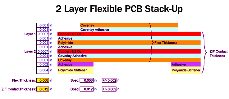
2-Layer Flexible PCB Stack-Up-
A two-layer flexible printed circuit board consists of several core components: a central base film, which is also called the laminate or substrate, two copper foils, up to four adhesive layers, and two protective covering layers.
The base film acts as the foundation, incorporating plated-through holes that create connections with the copper foil layers.
Adhesive layers are used to bond one copper layer to the base film and secure a protective coating onto both sides of the copper foil. These layers help maintain the stability of the PCB assembly, boosting its durability and offering protection from external factors.
How 2-Layer Flexible PCBs Compare to Other Flexible PCB Types?
To understand why 2-layer flexible PCBs are so versatile, it’s helpful to compare them with other types of flexible PCBs, such as single-sided and multi-layer versions. Let’s take a look at the differences:
Single-Sided PCB vs 2-Layer Flexible PCB-
Single-sided PCBs are simpler and typically consist of just one layer of copper on one side of the substrate. While they are cost-effective for basic circuits, they lack the capacity to handle more complex designs. In contrast, 2-layer flexible PCBs provide double the functionality by adding another layer of copper traces. This additional layer enables the creation of more intricate designs, offering greater component density and efficiency, making it a better choice for more advanced devices.
Multi-Layer PCB vs 2-Layer Flexible PCB-
On the other hand, multi-layer PCBs are used for highly complex designs requiring multiple layers of copper and intricate routing. While these PCBs offer excellent performance in high-frequency circuits or advanced computing applications, they are often rigid and require more space. 2-layer flexible PCBs offer a middle ground, providing more routing capabilities than single-sided versions while maintaining the flexibility that multi-layer PCBs lack.
Comparison Overview:
| Feature | Single-Sided PCB | 2-Layer Flexible PCB | Multi-Layer PCB |
| Layers | 1 | 2 | 3 or more |
| Flexibility | Low | High | Low |
| Design Complexity | Simple | Moderate | High |
| Cost | Low | Moderate | High |
The Competitive Advantage of 2-Layer Flexible PCBs in Various Industries
As industries continue to expand, the need for highly adaptable and efficient electronic solutions increases. 2-layer flexible PCBs are becoming a go-to solution in electronics manufacturing due to their ability to support complex designs in tight spaces, maintain long-term reliability, and offer performance at a reduced cost. These benefits are especially noticeable in sectors such as automotive electronics, medical devices, and consumer electronics, where precision, compactness, and consistency are core. Let’s take a closer look at how 2-layer flexible PCBs are making their mark across multiple industries.
Enhancing Product Performance with 2-Layer Flexible PCBs
The performance of an electronic device depends largely on the components used in its design. 2-layer flexible PCBs provide the ideal balance between compactness and reliable functionality. These PCBs are now widely used in automotive electronics, medical devices, and consumer electronics, where precision and consistent performance are highly valued.
In industries like automotive electronics, 2-layer flexible PCBs help support sensor systems and battery management solutions that require stable and accurate signal transmission. The flexibility of these PCBs ensures that they can withstand harsh conditions like vibration and temperature changes, which are typical in automotive environments.
Similarly, in medical devices, 2-layer flexible PCBs help to create compact circuits for applications like implantable devices and wearable health monitors. These PCBs enable more efficient designs that improve user comfort without compromising on functionality.
For consumer electronics, flexible PCBs enable devices to become smaller and more efficient, all while maintaining high performance. Applications such as smartphones, smartwatches, and wireless earphones benefit greatly from the versatility of 2-layer flexible PCBs.
Performance Comparison Table-
| Industry | Application | Benefit |
| Automotive | Sensor systems, battery management | Stability, accurate signal transmission |
| Medical Devices | Wearables, implantable devices | Compact designs, user comfort |
| Consumer Electronics | Smartphones, smartwatches, earphones | Smaller size, enhanced functionality |
Cost-Effective Manufacturing of 2-Layer Flexible PCBs
Manufacturing 2-layer flexible PCBs presents various cost-saving opportunities. Achieving cost-effective production is largely dependent on selecting the right materials and optimizing the manufacturing processes. Using the correct materials, such as polyimide or PET substrates, can reduce material costs while maintaining the necessary flexibility and strength. The choice of copper foil thickness is another factor that can influence costs, with thinner copper foil helping to minimize production expenses.
Additionally, adopting automated production techniques helps streamline the process, reducing labor costs and increasing manufacturing speed. This allows us to maintain quality and consistency in their production runs while keeping costs in check.
Cost Optimization Table-
| Factor | Consideration | Impact on Cost |
| Material Selection | Polyimide, PET substrates, Copper foil | Reduces material costs |
| Production Automation | Automated etching, lamination, testing | Reduces labor and operational costs |
| Process Efficiency | Improved production cycle times | Increases speed, reduces overall costs |
Meeting Industry-Specific Standards with 2-Layer Flexible PCBs
When designing 2-layer flexible PCBs for specific industries, compliance with various industry standards is essential. Standards such as IPC-2221, ISO9001, and UL certification ensure that the products are safe, reliable, and meet the necessary performance specifications.
IPC-2221 sets the standard for designing flexible PCBs that are both electrically and mechanically sound. ISO9001 focuses on maintaining consistent quality in the manufacturing process, ensuring that the PCBs meet the same high standard across different production batches. UL certification is required for products that need to meet specific fire safety and electrical safety guidelines, especially in automotive and medical applications.
By adhering to these standards, we can ensure that our 2-layer flexible PCBs meet the required safety, performance, and durability standards for their specific industries.
Industry Standards Table-
| Standard | Certification Authority | Focus Area | Industry Application |
| IPC-2221 | IPC | Design specifications for flexible PCBs | General electronics manufacturing |
| ISO9001 | International Organization for Standardization | Quality management system | All industries |
| UL Certification | Underwriters Laboratories | Fire resistance, electrical safety | Medical devices, automotive |
Design Considerations for 2-Layer Flexible PCBs
Designing a 2-layer flexible PCB requires a thoughtful approach to factors like material choice, circuit layout, and assembly processes. These design considerations can greatly affect the functionality, reliability, and efficiency of the finished product, ensuring it works smoothly across a variety of demanding applications.
When it comes to 2-layer flexible PCBs, certain features like flexibility, thermal performance, and signal integrity can have a direct impact on how well the PCB performs in real-world environments. Let’s take a closer look at the different aspects of designing a 2-layer flexible PCB to maximize its potential.
Optimizing Circuit Layout for 2-Layer Flexible PCBs
Efficient circuit layout forms the backbone of every well-performing 2-layer flexible PCB. By ensuring the right balance between trace width, via design, and signal integrity, we can achieve a compact yet robust PCB.
Trace width is one of the primary aspects to manage during the design phase. It directly affects how much current can pass through without causing overheating or breakdowns. The width is determined by the current load, copper thickness, and temperature. Tools and calculations based on these factors help find the ideal trace width to avoid potential issues with power delivery and reliability.
Next, via design plays a role in 2-layer flexible PCB performance. Microvias or blind vias are commonly used for their small footprint, which helps maintain the high-density design that flexible PCBs often require. Properly designed vias also avoid unnecessary stress points that might otherwise cause issues during flexing.
Additionally, signal integrity must be considered to ensure clean electrical signals without interference. Common solutions involve adding ground planes and shielding layers to prevent noise or degradation, especially in high-frequency applications such as consumer electronics and automotive devices.
Circuit Layout Design Table-
| Design Element | Consideration | Impact on Performance |
| Trace Width | Calculated based on current capacity | Prevents overheating and power loss |
| Via Design | Use of microvias or blind vias | Supports high-density layouts and reduces stress points |
| Signal Integrity | Use of ground planes, shielding | Reduces electrical noise and maintains signal clarity |
Material Selection for 2-Layer Flexible PCBs
Choosing the appropriate materials is a fundamental decision when designing a 2-layer flexible PCB. The materials selected can influence both the cost and the overall durability of the PCB, which is main factors in competitive industries.
For 2-layer flexible PCBs, the two most commonly used materials are polyimide and PET (polyethylene terephthalate). Polyimide is particularly known for its high-temperature stability, flexibility, and resistance to environmental stresses, making it suitable for challenging applications like automotive electronics and medical devices that require long-lasting performance.
On the other hand, PET provides a more cost-effective alternative while still offering decent flexibility, though it may not perform as well under higher thermal conditions. It’s often used in consumer electronics where performance can be balanced with lower production costs.
In addition, copper foil has a noticeable effect on the electrical performance of 2-layer flexible PCBs. Electrolytic copper is a common choice because of its excellent conductivity and long-lasting durability, making it well-suited for these designs. The copper’s thickness also influences both the electrical performance and thermal dissipation, helping to keep the PCB functioning effectively across a range of conditions.
Material Selection Comparison Table-
| Material Type | Key Features | Best Use Case |
| Polyimide | High flexibility, thermal stability, chemical resistance | Automotive, medical devices, aerospace |
| PET | Cost-effective, decent flexibility, moderate heat resistance | Consumer electronics, low-cost applications |
| Copper Foil | High conductivity, durable | Ensures efficient electrical performance |
Soldering and Assembly Techniques for 2-Layer Flexible PCBs
The soldering and assembly stages significantly influence the performance of a 2-layer flexible PCB. Given the flexible substrates used in these PCBs, extra attention is needed during assembly to preserve their structural integrity.
For 2-layer flexible PCBs, reflow soldering and wave soldering are typically used. Reflow soldering is effective for surface-mount devices, as it involves melting solder paste to attach components to the board. Wave soldering, on the other hand, is more suited for through-hole components, where the PCB passes through a molten wave of solder.
During the assembly process, thermal management is necessary to prevent any potential damage from thermal shock. Preheating the board before soldering helps to reduce stress, which can lead to cracks or other issues. Additionally, using low-temperature solders reduces the chance of damage to the PCB and its components during assembly.
Soldering and Assembly Process Table-
| Technique | Description | Recommended Use Case |
| Reflow Soldering | Melting solder paste with heat | Ideal for surface-mount components |
| Wave Soldering | Passing PCB through molten solder | Best for through-hole components |
| Preheating | Heating the PCB before soldering | Reduces risk of thermal stress and improves joint quality |
2-Layer Flexible PCB Manufacturing Process
The manufacturing process of 2-layer flexible PCBs consists of several precise steps that transform raw materials into functional electronic circuits. Each stage contributes to the overall performance and reliability of the final product, which is used in everything from consumer electronics to medical devices and automotive applications. In this section, we’ll take a closer look at each phase of the process, shedding light on the methods and considerations that drive quality and efficiency.
Step-by-Step Overview of the 2-Layer Flexible PCB Manufacturing Process
Creating 2-layer flexible PCBs involves several stages, each requiring a high level of precision. From etching to lamination, the following steps outline the journey of a flexible PCB from raw material to finished product:
●Material Preparation: The first step involves selecting the appropriate flexible substrates such as polyimide or PET. These materials are cleaned and treated to ensure they adhere well to the next layers.
●Circuit Pattern Printing: A photoresist layer is applied to the substrate, and the circuit design is transferred using photolithography. This process defines the layout of the conductive traces that form the PCB.
●Etching: The etching process removes excess copper from the substrate, leaving behind the desired traces. This step defines the electrical pathways on the board, ensuring proper connectivity and functionality.
●Lamination: During lamination, the flexible substrates are bonded together using an adhesive. This ensures that the layers stay securely in place throughout the lifetime of the PCB.
●Drilling: Laser drilling is used to create small holes or vias, allowing for connections between the two layers. The precision of the drill ensures that the vias align perfectly, ensuring good electrical connection.
●Final Touches: After lamination and drilling, a soldermask is applied to protect the traces. The board is then tested and inspected for any defects.
PCB Manufacturing Process Table-
| Stage | Description | Key Considerations |
| Material Preparation | Cleaning and preparing flexible substrates | Ensures surface adhesion and reliability |
| Circuit Pattern Printing | Transferring circuit design to photoresist | High-precision photolithography |
| Etching | Removing unwanted copper from the substrate | Ensures correct trace width and integrity |
| Lamination | Bonding substrates with adhesive | Critical for layer adhesion and durability |
| Drilling | Creating vias to connect layers | Laser precision for accurate via placement |
| Final Touches | Applying protective soldermask layer | Prevents shorts and maintains reliability |
Advanced Manufacturing Techniques for 2-Layer Flexible PCBs
The demand for smaller, more precise electronic devices has driven the evolution of manufacturing techniques used for 2-layer flexible PCBs. These techniques include laser drilling and automated production, both of which improve the overall speed and accuracy of the manufacturing process.
●Laser Drilling: Laser drilling allows for the creation of vias with exceptional precision, which is especially useful when designing high-density interconnects (HDI). These small holes provide the necessary channels for electrical signals, ensuring that even compact designs function effectively.
●Automated Manufacturing: With automated production lines, we can speed up the process while ensuring greater consistency. Tasks such as etching, drilling, and soldering can be carried out by machines with a level of precision that human workers simply cannot match. This also allows for fewer errors, increasing the overall reliability of the finished 2-layer flexible PCBs.
●Optical Inspection: To ensure that every board meets the required quality standards, automated optical inspection (AOI) systems are used. These systems check for defects such as misaligned traces or incorrect via placements, making sure that all products meet the strict specifications.
Advanced Manufacturing Techniques Table-
| Technique | Description | Benefits |
| Laser Drilling | Uses lasers to precisely drill small vias | High-precision, ideal for high-density designs |
| Automated Manufacturing | Uses robotic systems to handle PCB production | Faster and more accurate than manual methods |
| Optical Inspection | Automated visual inspection of boards | Detects defects and ensures high-quality standards |
Common Challenges in 2-Layer Flexible PCB Design and Manufacturing
When it comes to designing and manufacturing 2-layer flexible PCBs, several challenges arise at both the design and production stages. These obstacles, ranging from trace width constraints to material selection, require skilled engineers and advanced technologies to overcome. By addressing these challenges, we can ensure our products meet the specific requirements of industries like consumer electronics, medical devices, and automotive applications. Let’s dive into these common design and manufacturing challenges, and explore how to tackle them efficiently.
Design Limitations and Solutions for 2-Layer Flexible PCBs
2-layer flexible PCB designs come with a unique set of limitations that we must work around. For example, trace width and via size are often constrained due to the flexible nature of the materials used. Additionally, the density of circuits and components must be balanced carefully to avoid any performance degradation. But no need to panic — there are practical solutions for these challenges!
●Trace Width and Via Size: When designing a flexible PCB, the width of the traces is determined by the amount of current the trace needs to carry. For 2-layer flexible PCBs, maintaining a minimum trace width without compromising electrical performance can be tricky, especially in compact designs. Smaller via sizes can also impact the performance and manufacturability, especially when it comes to laser drilling techniques.
Solution: To overcome these challenges, we often rely on advanced design software that can simulate various trace widths and via sizes to find an optimal balance between performance and manufacturability. In some cases, buried vias and microvias are used to reduce via size without compromising on performance.
●Circuit Density: The flexibility of polyimide and PET substrates means that there’s often less room for circuit pathways than with rigid PCBs, but that doesn’t mean circuit density has to suffer. We need to carefully evaluate component placement to ensure efficient use of space.
Solution: we can leverage techniques like layer stacking, where a second layer is used to reduce the footprint, and advanced routing methods to ensure that components fit without sacrificing performance.
Design Limitations Table-
| Limitation | Description | Solution |
| Trace Width | Limited by current-carrying capacity and space constraints | Use simulation software to find optimal widths |
| Via Size | Smaller vias are harder to manufacture and may limit signal integrity | Use microvias or buried vias |
| Circuit Density | Limited space for high-density components | Use stacking and efficient routing techniques |
Reliability Testing for 2-Layer Flexible PCBs
Testing the reliability of 2-layer flexible PCBs is an indispensable part of ensuring they perform well under real-world conditions. These PCBs must endure mechanical stress, extreme temperatures, and exposure to various environmental factors. Without thorough testing, you risk unpredictable failures that can affect the device’s overall lifespan.
●Mechanical Stress Testing: Flexible PCBs are designed to bend and flex, making them reliable for applications in wearables and automotive electronics. However, repeated bending can lead to fatigue failures. Mechanical stress testing simulates these bending cycles to ensure that the PCB remains durable over time.
●Thermal Cycling: Another important test for 2-layer flexible PCBs is thermal cycling, where the PCB is exposed to rapid temperature changes to mimic real-world environmental conditions. This test is especially useful for applications in automotive and medical devices, where products must perform consistently across a wide temperature range.
●Environmental Testing: Finally, exposure to humidity, moisture, and chemicals can lead to degradation of the PCB’s materials. Environmental tests ensure that 2-layer flexible PCBs withstand harsh conditions without performance loss.
Reliability Testing Table-
| Test Type | Description | Importance |
| Mechanical Stress | Bending the PCB to simulate wear over time | Ensures flexibility without failure |
| Thermal Cycling | Rapid temperature changes to simulate environment | Prevents failure under temperature extremes |
| Environmental Tests | Exposure to moisture, humidity, and chemicals | Ensures durability in challenging conditions |
Materials and Process Innovations to Overcome Challenges
To overcome the design and manufacturing challenges inherent in 2-layer flexible PCBs, the industry has seen some exciting innovations in both materials and processes. These advancements enable flexible PCBs to achieve higher performance, better durability, and greater ease of manufacturing.
●Flexible Substrates: The development of advanced flexible substrates such as polyimide, PET, and PEN has enabled engineers to create PCBs that can bend and stretch without compromising their electrical performance. These materials are often used in wearables and medical devices where flexibility is a must.
●Adhesive Technologies: Adhesives are integral in bonding the layers of 2-layer flexible PCBs. Recent advancements in adhesive technologies have improved the ability to create strong bonds while preserving the flexibility of the PCB. This is especially useful for flexible substrates that are exposed to challenging mechanical and thermal conditions.
●Manufacturing Process Innovations: One of the biggest innovations in 2-layer flexible PCB manufacturing has been the development of laser drilling techniques. This allows us to create vias that are both smaller and more precise than ever before. Additionally, the use of automated inspection systems ensures that every 2-layer flexible PCB is up to spec.
Materials and Process Innovations Table-
| Innovation | Description | Impact |
| Flexible Substrates | Materials like polyimide and PET that allow bending without loss of electrical function | Enhances flexibility and durability |
| Adhesive Technologies | New adhesives that offer strong bonds while maintaining flexibility | Increases product lifespan and reliability |
| Laser Drilling | Precision drilling techniques for smaller, more accurate vias | Allows for compact designs with fewer defects |
Quality Control and Testing for 2-Layer Flexible PCBs
When working with 2-layer flexible PCBs, quality control and testing are essential steps in the production process. These procedures verify that each PCB meets the necessary standards for durability, performance, and consistency. For engineers, manufacturers, and users, understanding the testing methods for flexible PCBs ensures that the final product functions properly across various conditions, maintains steady performance, and suits the intended application. Let’s explore how these tests are carried out and how they help ensure the reliability and functionality of the finished PCBs.
Ensuring Durability with Environmental and Mechanical Testing
Environmental and mechanical testing is the backbone of any flexible PCB testing regime. Flexible PCBs, due to their inherent design and materials, are often exposed to harsh conditions—temperature fluctuations, humidity, physical stress, and even vibration. These tests ensure the circuit boards maintain integrity even under tough conditions.
●Temperature Cycling: By subjecting 2-layer flexible PCBs to extreme temperature changes (from hot to cold), we can simulate how the boards will perform in environments with varying thermal conditions.
●Humidity Exposure: This test measures how moisture affects the PCB’s functionality, ensuring that it remains reliable even in humid environments.
●Vibration Testing: Especially relevant for automotive or aerospace applications, this test evaluates how the PCB holds up under vibrations, making sure it doesn’t experience mechanical failure.
Table 1: Common Environmental Testing Parameters for 2-Layer Flexible PCBs
| Test Type | Conditions Tested | Purpose |
| Temperature Cycling | -40°C to +125°C | Evaluate performance under thermal stress |
| Humidity Exposure | 95% RH at 85°C for 1000 hours | Assess long-term moisture effects |
| Vibration Testing | Frequency: 10-500Hz | Ensure PCB durability in vibration-prone environments |
These tests provide crucial data on the durability and long-term performance of 2-layer flexible PCBs, making sure they can handle demanding environments.
Visual and Automated Inspection for High-Quality 2-Layer Flexible PCBs
To ensure high-quality production, we can rely on both visual and automated inspection systems to detect defects before the product reaches the market. Manual inspection still plays a role, but it’s the integration of automated systems that allows for scalability and precision.
●Visual Inspection: This is often the first step where operators perform detailed checks on the surface of the PCB to identify any obvious defects like misplaced traces or voids.
●Automated Optical Inspection (AOI): AOI uses cameras and software to automatically scan PCBs for defects such as misalignment, component placement issues, or soldering problems. These systems help reduce human error and speed up the inspection process.
●X-Ray Inspection: For complex boards with hidden layers, X-ray inspection can be used to visualize internal structures and confirm that vias and interconnections are correctly made.
Accelerating Time-to-Market with Rapid Prototyping for 2-Layer Flexible PCBs
In today’s competitive manufacturing landscape, time-to-market is often a deciding factor in product success. With 2-layer flexible PCBs, rapid prototyping becomes a powerful tool for accelerating development cycles.
●Prototyping: Early prototyping allows us to test out their designs quickly, validate the performance of circuits, and make adjustments before committing to full-scale production.
●Quick Turnaround: By using advanced manufacturing processes like additive printing or laser cutting, we can produce prototypes of 2-layer flexible PCBs in days, not weeks, helping bring products to market faster.
●Design Refinement: we can test and refine the design, ensuring that any potential manufacturing or design flaws are addressed early in the development process.
Table 2: Time-to-Market Comparison with Traditional vs. Rapid Prototyping for 2-Layer Flexible PCBs
| Process | Traditional Manufacturing | Rapid Prototyping |
| Lead Time | 4-6 weeks | 3-7 days |
| Design Iterations | 1-2 | 3-4 |
| Cost of Prototypes | High | Moderate |
Rapid prototyping can shave off significant time from the design-to-manufacture cycle, allowing us to optimize their 2-layer flexible PCBs faster and more efficiently.
How to Choose the Right Manufacturer for 2-Layer Flexible PCBs?
When choosing a manufacturer for 2-layer flexible PCBs, there are several factors to consider to ensure the final product meets your specifications. A reliable manufacturer should demonstrate strong expertise in flexible PCB technology, a proven history of delivering quality products, and the capability to handle custom designs. Let’s break down the key criteria for selecting a manufacturer who aligns with your needs.
Selecting a PCB Manufacturer with Expertise in Flexible PCBs
Choosing a manufacturer with a solid background in flexible PCB production is essential. You’ll want a partner who can manage the intricacies of flexible circuit design and production, from material selection to the final assembly. An experienced manufacturer will be able to handle diverse challenges in flexible PCB production and deliver on your project requirements effectively.
| Criteria | Description |
| Experience in Flexible PCB Design | Look for a manufacturer with a proven track record in flexible PCB production. |
| Material Expertise | Ensure the manufacturer is familiar with the materials commonly used in flexible PCBs, like polyimide and PET. |
| Customization Options | The manufacturer should offer flexibility in custom designs to meet specific project needs. |
| Certifications | Check for industry-standard certifications (e.g., ISO 9001) to ensure the manufacturer follows quality standards. |
Evaluating Cost-Effectiveness and Lead Time for 2-Layer Flexible PCBs
Cost-effectiveness and lead time are core factors when choosing a flexible PCB manufacturer. By considering these aspects, you can ensure the supplier meets your budget and timeline while maintaining the required standards. This is particularly useful for projects with tight deadlines or specific cost constraints.
| Factor | Considerations |
| Cost Structure | Make sure the manufacturer offers transparent pricing and works within your budget. |
| Lead Time | Evaluate the lead times offered by the manufacturer and ensure they can meet your project schedule. |
| Production Capacity | Confirm that the manufacturer can handle your project’s scale without compromising quality or delivery times. |
Ensuring Consistent Quality Control and Testing for 2-Layer Flexible PCBs
Quality control and testing are fundamental to ensuring that your 2-layer flexible PCBs will function as intended. Ensure that the manufacturer performs thorough testing at every stage of production, from initial design to final product. Techniques like automated inspection, mechanical testing, and environmental stress testing help identify defects and guarantee long-term reliability.
| Testing Process | Description |
| Automated Visual Inspection | This step detects any visual defects on the surface of the PCB. |
| Mechanical Testing | Includes tests for flexural strength, stress resistance, and durability. |
| Environmental Testing | Involves temperature cycling, humidity testing, and vibration testing to ensure the PCB can withstand extreme conditions. |
FAQs for 2-layer flexible PCBs
1.How do you determine the optimal trace width for a 2-layer flexible PCB?
Trace width is calculated based on the current carrying requirements, material properties, and desired temperature rise, ensuring reliable performance without excessive heat.
2.What are the most common failure modes for 2-layer flexible PCBs?
Common failure modes include flexural cracks, delamination, trace failure, and poor solder joints, often caused by improper design or handling during assembly.
3.How does the bending radius affect the performance of a 2-layer flexible PCB?
The bending radius determines how tightly the PCB can bend without damaging its traces or causing mechanical failure. A smaller radius increases the risk of damage.
4.Are 2-layer flexible PCBs compatible with surface mount technology (SMT)?
Yes, 2-layer flexible PCBs are compatible with SMT, but special care must be taken during the soldering process to avoid damage due to flexibility.
5.How do you handle high-voltage circuits on 2-layer flexible PCBs?
High-voltage circuits on flexible PCBs require proper spacing, insulation, and specialized materials to ensure safe operation.
6.What is the maximum size for 2-layer flexible PCBs?
The maximum size is influenced by the manufacturing process and equipment capabilities, but flexible PCBs typically range from a few millimeters to several meters in size, depending on the application.


