
Single or double layer flexible PCBs have constraints in meeting the power and speed needs of more intricate projects making them unsuitable, for high demand applications. In cases 4 layer flexible PCBs provide a crucial solution offering numerous advantages compared to single or double sided PCBs.
To avoid costly mistakes in the future, it is essential to have a comprehensive understanding of 4-layer flex PCB materials, design considerations, applications, benefits and layout. This article aims to provide detailed and insightful information on each aspect of 4-layer rigid-flex PCB. Are you ready to explore? Let’s delve into it!
What is 4 Layer Flex PCB?
Flexible PCB circuit boards are composed of electronic circuits mounted on flexible plastic substrates, allowing for versatile and adaptable designs. The construction of these flexible circuit boards can be achieved via the technique of screen-printing silver circuits onto polyester materials.
4 layer flex PCB incorporate four conductive layers, usually fabricated with a material termed Polyimide. While FR4 is an option, Polyimide is favored due to its assorted benefits. Known for its superior thermal stability, Polyimide ensures that 4-layer flex PCB can endure elevated temperatures. As a result, these PCBs are extensively employed in applications that operate at high temperatures.
Furthermore, Polyimide provides significant flexibility, facilitating the mounting of electronic devices that would be challenging to assemble on rigid boards. This flexibility streamlines the design process and allows for intricate designs that would be impossible to achieve with rigid circuit boards. Additionally, the use of Polyimide reduces the overall weight of printed circuit boards.
Materials Used in Making 4 Layer Flex PCB
The materials used in 4-layer flex PCB play a crucial role in their longevity and effectiveness. These materials enable the PCB to meet the demands of various applications. The materials integral to 4-layer flex PCB can essentially be divided into three principal categories
Base Material:
In flexible circuit boards, the foundational element is the base material. For rigid-flex PCB, a flexible polymer film discharges this foundational role. Typically, the substrate material is polyimide, renowned for its superior flexibility and heat resilience. Polyimide provides the necessary characteristics for rigid-flex PCB, reducing board thickness compared to rigid boards. Its flexibility aids in averting common breakages found in rigid boards. An additional benefit of polyimide is its non-reliance on adhesive for fastening copper.
Adhesive:
Adhesive materials are used to form bonds in the PCB. When polyimide is used as the base material in rigid-flex PCB, the choice of adhesive is critical as it can affect the laminate’s performance. Using polyimide adhesives can present certain challenges, so alternative adhesive materials from different polymer families are often used. The thickness of the adhesive in flex circuits varies depending on the specific application requirements.
Conductive Material:
The conductive material is a key component of 4-layer flex PCB, particularly in industrial control equipment and industrial applications. Copper is commonly used as the conductive material in these PCB. Copper offers excellent electrical properties, is available in various thicknesses, and is cost-effective, making it highly desirable for 4-layer flex circuit boards. Copper foils come in two main types: electrodeposited and rolled/wrought. Additionally, there is a demand for thinner copper foils in modern applications.
By carefully selecting and utilizing these materials, 4-layer flex PCB can be optimized for performance and durability in a wide range of applications.
4 Layer Flex PCB Stack-up and Configurations
In adherence to regulations, the minimum total thickness of the thinnest variant of a 4-layer PCB measures at 0.282 mm with a tolerance of +/- 0.03 mm. However, it is worth noting that there are alternative options available, with the maximum thickness reaching 0.45 mm. The thickness of copper employed in the PCB holds significance as it directly impacts the trace width and current carrying capacity
Stack-up:
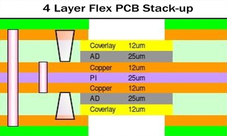
The composition of the multilayer flex board’s stack-up consists of the following layers:
1. Coverlay: This layer comprises polyimide material combined with adhesive.
2. Copper trace: A layer featuring copper traces, accompanied by an adhesive layer.
3. Another layer of copper trace: Similar to the previous layer, this one also includes copper traces and an adhesive layer.
4. Bottom layer of coverlay: This layer is composed of coverlay, serving as the bottom-most component of the stack-up.
By following this stack-up arrangement, the PCB achieves the desired structure and functionality.
Configurations:
Symmetrical Arrangement:
In a layout the PCB configuration follows a specific sequence beginning with a coverlay followed by a signal layer (Layer 1) ground plane (Layer 2) flexible core dielectric, another signal layer (Layer 3) ground plane (Layer 4) and ending with yet another coverlay. This structured arrangement effectively controls interference (EMI) through the integration of ground plane shielding and maintaining parallel layer configurations on both sides of the core. This design approach helps minimize EMI emissions and contributes to enhancing signal reliability.
Asymmetrical Arrangement:
In a layout the PCB structure comprises a coverlay then transitions to a signal layer (Layer 1) ground plane (also Layer 1) power layer, flexible core dielectric, another ground plane (Layer 2) followed by a signal layer (Layer 3) and concluding with an additional coverlay. This setup is strategically designed to create separation between signals by positioning power and ground planes on opposite sides of the core dielectric. By establishing this separation, between power and ground planes this design effectively reduces interference and crosstalk across signal paths ultimately improving overall signal integrity.
High-Speed Arrangement:
Pertaining to the high-speed layout, the PCB structure consists of a coverlay, followed by a signal layer (Layer 1), a ground plane (Layer 1), an additional signal layer (Layer 2), a flexible core dielectric, yet another signal layer (Layer 3), a secondary ground plane (Layer 2), and concluding with another coverlay. This configuration is meticulously designed for high speed signals necessitating impedance control. The exterior layers are explicitly assigned to transport these high speed signals, while power and ground planes are strategically oriented to act as steady reference planes. This setup aids in upholding signal integrity, mitigating signal loss, and managing impedance, thereby ensuring trusty high-speed signal transmission.
Please note that the specific arrangement and layer configuration of a PCB can vary depending on the design requirements and the intended application. These examples illustrate common approaches used in PCB designs to achieve specific goals related to EMI control, signal isolation, and high-speed signal transmission.
Benefits of 4 Layer Flex PCB
Despite the extensive global utilization of rigid printed circuit boards, flexible printed circuit boards proffer unique benefits. Here are some principal advantages:
Compatibility: 4-layer flex PCB are highly compatible with a wide range of connectors and components, surpassing the compatibility of rigid PCB.
Stability and Reliability: Flexible circuit boards manifest superior stability and dependability relative to their rigid PCB counterparts. Owing to a diminished count of interconnects and solder junctions, the probability of errors is significantly lessened, thereby enhancing the overall reliability.
Weight and Space Efficiency: Flex PCB are lightweight and occupy significantly less space than traditional PCB. They require only around ten percent of the space and weight, leading to reduced transportation costs, greater installation flexibility, and easier packaging processes.
Higher Circuit Density: 4-layer flex PCB offer higher circuit density, allowing them to meet the requirements of dynamic flexing applications.
Wide Temperature Range: Flex PCB have a wider temperature range, enabling them to operate under higher currents and enhancing the lifespan of electronic components.
Improved Signal Quality and Impedance Control: Four-layer flex PCB provide enhanced signal quality, precise impedance control, and robust operation, giving them an advantage over other alternatives available in the market.
These advantages make 4-layer flex PCB a favorable choice in various industries, offering improved performance, reliability and efficiency for electronic systems and devices.
Challenges in 4 Layer Flex PCB Fabrication
The production of 4-layer flex PCB presents inherent challenges despite their significant advantages. These difficulties include:
Achieving fine lines and spaces on multiple flexible layers: Ensuring precise and narrow traces on multiple flexible layers is a complex task.
Holding tight layer-to-layer registration through all photolithography stages: Maintaining accurate alignment between different layers throughout the photolithography process is crucial but can be challenging.
Producing a high density of buried and blind microvias with thin dielectric: Creating numerous small-diameter microvias that are buried or blind, while maintaining a thin dielectric layer, poses a manufacturing challenge.
Preventing lifted lands or cracked barrel plating on during flexing: The flexing action can potentially cause lifted lands or cracked barrel plating on PTHs, necessitating careful design and material selection.
Maintaining reliable coverlayer and stiffener adhesion through dynamic flexing: Ensuring consistent adhesion between the coverlayer, stiffener, and flexible layers during dynamic flexing is critical for the PCB’s long-term reliability.
Controlling characteristic impedance across multiple flex layers: Achieving consistent characteristic impedance across different flex layers is a complex task due to variations in materials and geometries.
Managing thermomechanical stresses and fatigue-prone areas: Flex PCB are subjected to thermomechanical stresses, which can lead to fatigue and failure in certain areas. Managing these stresses is essential for ensuring long-term reliability.
Qualification testing of impedance shifts under long-term flex cycling: Conducting thorough qualification testing to assess impedance shifts under prolonged flex cycling is necessary to validate the PCB’s performance and reliability.
Ensuring flex fold and bend cycle life reaches millions of cycles: Flex PCB must be designed and manufactured to withstand millions of cycles of flexing and bending without degradation or failure.
Addressing these challenges requires expertise in design, material selection, manufacturing processes, and thorough testing to ensure the production of high-quality and reliable 4-layer flex PCB.
4 Layer Flex Design Recommendations
Plan Stack-up Arrangement: Carefully arrange the stack-up to isolate critical signals using ground planes, allowing for better signal integrity and minimizing interference.
Impedance Matched Traces and Shielding: Use impedance matched traces for high-speed signals and provide adequate shielding to minimize signal degradation and electromagnetic interference.
Model Performance under Dynamic Bending Conditions: Consider the effects of bending on signal integrity and impedance, and simulate the performance under various bending scenarios to ensure reliable operation.
Adjust trace dimensions in flexing areas: Increase the trace and space dimensions in areas that undergo flexing to prevent mechanical stress and ensure durability compared to rigid sections.
Incorporate strain relief structures: Include strain relief structures at the interfaces between rigid and flex sections to minimize stress concentration and enhance mechanical reliability.
Utilize thermal reliefs: Implement thermal reliefs for solder joints to reduce stress on the flex PCB, especially during temperature variations, minimizing the risk of solder joint failure.
Add stiffeners or covers: Integrate stiffeners or covers at connection points or areas requiring extra rigidity to enhance mechanical stability and prevent damage during handling or assembly.
Component placement: Maximize the distance of components from high flex zones to avoid potential damage or strain on sensitive components during bending or flexing.
Controlled bend radii: Specify multiple controlled bend radii rather than arbitrary flexing to ensure consistent and reliable performance during repeated flexing.
Check for acid traps: Review layouts for susceptibility to acid traps during fabrication, ensuring proper copper etching and avoiding issues related to acid entrapment.
Microvia capture pads: Specify microvia capture pads with a 1:1 aspect ratio to ensure reliable connections and minimize the risk of via failures.
Consider shielding, insulation, and abrasion resistance: Take into account the need for shielding, insulation, and abrasion resistance in the stack-up design, depending on the application requirements and environmental conditions.
By following these guidelines, designers can enhance the performance, reliability, and manufacturability of 4-layer flex PCB, meeting the specific needs of their applications.
Applications of 4 Layer Flex PCB
Flex PCB offer several advantages such as reduced weight and a low bend radius, making them highly suitable for implementation in medical devices and industrial control equipment. In the automotive industry, these flexible PCB find effective utilization in vehicle interior control equipment, ABS systems, dashboards, and other related applications.
Furthermore, flex boards provide a comprehensive solution for the consumer electronics industry, serving as a versatile component in various devices such as calculators, motion monitors, cameras, keyboards, tablets and more.
Within the medical sector, flex PCBs are employed for interconnections involving resistors, circuits, and capacitors, enabling seamless integration and functionality. The impressive power, thinness, and stiffener capabilities of flex PCB make them an ideal choice, particularly in aeronautical and marine equipment applications.
In the mobile phone market, layer flex PCB hold a central position and remain a popular choice. Their assembly process, along with the soothing green color on one or both sides, adds visual appeal. In compact devices like cell phones, these flex PCB facilitate multiple interconnections, enhancing overall efficiency and performance.
Conclusion
The utilization of 4-layer flex PCB technology offers the opportunity to create innovative products that exhibit high routing density while maintaining dynamic flexing capabilities. However, realizing the full potential of this technology necessitates careful consideration of stack-up configurations, meticulous process control, and proficient flex design techniques. Collaborating with an experienced flex PCB manufacturer-JarnisTech, renowned for their expertise in 4-layer technology, empowers designers to maximize the benefits of 4-layer flex PCB and cultivate state-of-the-art solutions for the integration of flexible electronics across diverse industries.


