
In the tech realm of electronics, edge connectors in printed circuit boards (PCBs) are the backbone of many systems. Often flying under the radar, these connectors play a vital part in keeping everything running smoothly. So, what’s the secret sauce behind their performance? You got it—gold plating. Far from just a flashy finish, gold plating ensures connectors have longevity, optimal performance, and reliability in tough situations.
Understanding Edge Connectors in PCBs
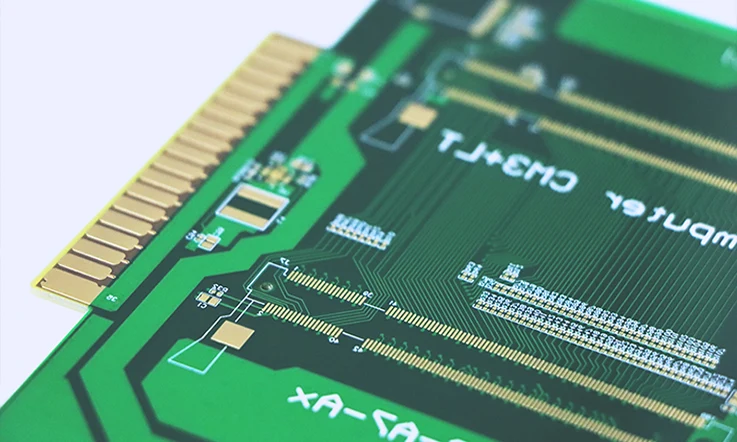
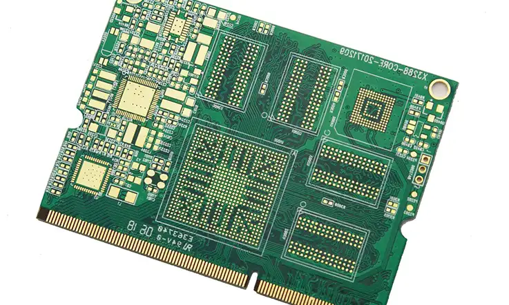
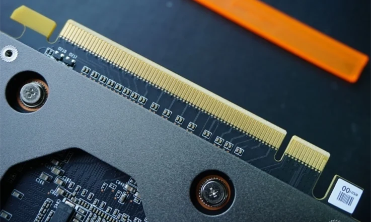
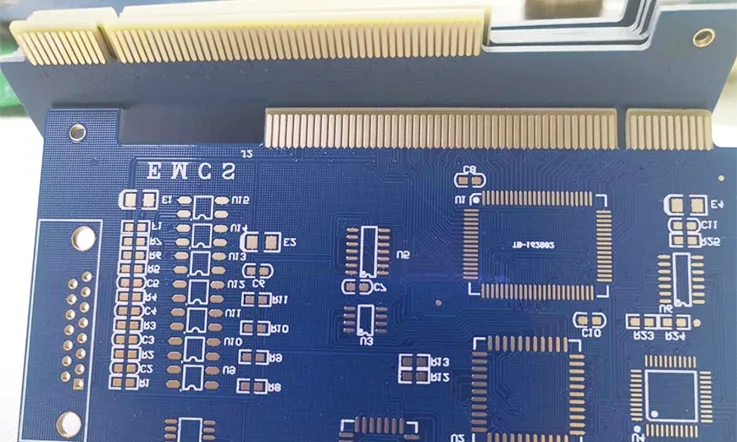
Edge connectors are those metal contacts located at the edges of a printed circuit board (PCB), serving as the critical link between the board and other components. Imagine them as the handshake between different parts of a device, allowing signals and power to flow seamlessly. Whether it’s in your smartphone, a car’s navigation system, or a high-performance server, these connectors ensure that data and power travel from point A to point B without any hiccups.
Why Edge Connectors Matter?
These connectors take quite a beating, especially in scenarios where they’re plugged in and unplugged repeatedly, like in testing setups or modular systems. Here’s where gold plating steps in to save the day. Gold isn’t just a shiny accessory; it brings some serious advantages to the table:
●Outstanding Conductivity: Gold is a superstar when it comes to conducting electricity. It keeps signal loss at bay, which is crucial for high-speed applications.
●Corrosion Resistance: Gold’s natural resistance to oxidation and corrosion means it won’t tarnish or degrade, even in challenging environments. This feature is vital in ensuring edge connectors remain reliable over time.
●Durability: With gold plating, these connectors can withstand frequent usage without losing their performance edge. Think of it as putting on a tough coat that protects against wear and tear.
Gold Plating Techniques for Edge Connector PCBs
When it comes to gold plating techniques for edge connector PCBs, there are several approaches to consider. Each method has its own advantages and drawbacks, depending on the specific needs of the PCB. Let’s dive into the most common techniques:
Hard Gold Plating
Often referred to as “electrolytic hard gold,” this method involves applying a thick layer of gold over a nickel barrier using electric current. It’s the go-to choice for edge connectors due to its impressive wear resistance. This technique is perfect for components that will face a lot of mechanical stress, as the gold layer can handle multiple insertions and removals without a hitch. This reliability is key for applications like military or aerospace, where performance under pressure is a must.
Selective Gold Plating
Selective gold plating is a savvy technique where only the necessary contact points receive a coating of gold, while the rest of the PCB stays free of the pricey material. This method helps keep costs manageable while still delivering the advantages of gold where it matters most—like on those edge connectors. It’s a smart choice for consumer electronics, where budget constraints are always a factor.
Full-Body Gold Plating
In some specialized applications, particularly in high-end circuits, full-body gold plating is used to coat the entire PCB. This method ensures every part of the board benefits from gold’s protective properties. However, it’s often overkill for most consumer gadgets, where cost is a big deal. For example, in advanced computing systems or medical devices, full-body plating may be worth the investment to avoid any signal loss or degradation over time.
Summary Table of Gold Plating Techniques
| Technique | Pros | Cons | Best For |
| Hard Gold Plating | Excellent wear resistance | Higher cost | Military, aerospace applications |
| Selective Gold Plating | Cost-effective, targets critical areas | Limited coverage | Consumer electronics, modular systems |
| Full-Body Gold Plating | Uniform protection for the entire PCB | Expensive and often unnecessary | High-end circuits, specialized devices |
Why Gold Plating is Essential for Edge Connector PCBs?
Gold plating is a key player in the world of edge connector PCBs, thanks to its impressive properties that boost durability, electrical performance, and resistance to environmental challenges. Grasping the significance of gold in this realm helps designers and manufacturers craft more reliable and long-lasting edge connectors across various applications.
1. Superior Conductivity
One of the standout features of gold plating on edge connectors is its exceptional electrical conductivity. Gold shines where other metals might fall flat, exhibiting low electrical resistance that enables efficient signal transmission with minimal loss. This factor is especially significant in high-speed data applications, where keeping the signal intact is a must. Gold plating ensures solid and stable contact points between the edge connector and its mating counterpart, cutting down on interruptions or signal hiccups.
2. Corrosion Resistance
Gold is a champ when it comes to resisting oxidation and corrosion. Unlike metals like copper or tin, which can tarnish over time, gold acts as a trusty shield against environmental factors. In areas where moisture, humidity, or air exposure could spell trouble for other materials, gold provides a protective layer for edge connectors. This feature is particularly handy in industrial or outdoor settings where PCBs face tough conditions. Gold-plated edge connectors keep their reliability and performance intact for the long haul, even in the face of adversity.
3. Mechanical Wear Resistance
Edge connectors often endure repeated insertion and removal, leading to wear and tear over time. That’s where hard gold plating comes in, offering outstanding durability and wear resistance. This durability enables connectors to handle frequent use without suffering significant degradation. Such resilience is vital for PCBs in high-reliability applications like military or aerospace, where the connectors must hold their own against constant engagement.
4. Longevity and Cost Efficiency
While gold is pricier than many other metals, its application in edge connectors can lead to long-term savings. The durability and corrosion resistance of gold plating cut down on the need for frequent replacements or repairs, keeping maintenance costs in check. This makes gold a smart investment, especially for devices where reliability is non-negotiable—think medical equipment or automotive electronics.
5. Minimizing Signal Interference
Gold plating also plays a key part in reducing signal interference, which is essential for high-frequency applications. The smooth, conductive surface provided by gold-plated connectors helps electrical signals pass through without distortion or loss. This quality is why gold-plated edge connectors are the go-to choice in critical applications where precision and reliability matter.
Table: Benefits of Gold Plating for Edge Connector PCBs
| Benefit | Description | Application Examples |
| Superior Conductivity | Low electrical resistance for efficient signal transmission | High-speed data applications |
| Corrosion Resistance | Protects against oxidation and environmental factors | Outdoor electronics, industrial PCBs |
| Mechanical Wear Resistance | Durable against repeated use | Military, aerospace connectors |
| Longevity | Reduces replacement and maintenance costs | Medical equipment, automotive electronics |
| Minimizing Signal Interference | Ensures clear signal transmission | High-frequency applications |
Types of Gold Plating Used in Edge Connector PCBs
Selecting the right gold plating method for edge connector PCBs is no small potatoes, as each method brings its own set of benefits tailored to different applications and requirements. Let’s dive into the most commonly used types of gold plating for edge connectors, breaking down their strengths and typical use cases.
1. Electrolytic Gold Plating
Electrolytic gold plating is one of the most popular methods for edge connector PCBs, known for its ability to deposit a thick and robust layer of gold. This process involves passing an electric current through a solution, allowing gold ions to stick to the connector’s surface. Here’s what you can expect:
Durability and Strength: Electrolytic gold offers top-notch wear resistance, which is a must for connectors that see a lot of action, like those in military or aerospace applications. Think of it as giving your connectors a suit of armor.
Consistent Conductivity: This method ensures low electrical resistance, leading to stable signal transmission over time. It’s like having a well-oiled machine; everything just runs smoother.
Gold Thickness: Typically, the thickness ranges from 0.76 to 2.54 microns, making it ideal for high-reliability connectors that undergo repeated mechanical engagement. This technique is often called hard gold plating due to the hardness achieved by co-depositing cobalt or nickel with the gold.
2. Electroless Nickel Immersion Gold (ENIG)
ENIG stands out as another popular method, and it’s a bit different from electrolytic gold since it doesn’t need an electric current. Instead, this method involves first depositing a layer of nickel on the PCB, which acts as a barrier, followed by a thin immersion gold layer. Here’s the scoop:
Cost-Effective: ENIG is generally more economical because the gold layer is thinner, typically between 0.05 and 0.1 microns. This makes it a smart choice for consumer electronics where budget matters.
Smooth Surface: This method produces a slick surface that ensures solid, consistent electrical contact. It’s like having a freshly waxed car; it looks good and performs better.
Corrosion Resistance: While it may not have the same durability as hard gold plating, its high corrosion resistance makes it a solid option for high-density PCBs.
3. Immersion Gold
Immersion gold plating uses an autocatalytic process where gold replaces metal atoms on the PCB’s surface, usually nickel. Here’s how it works:
Selective Plating: This method allows for targeted plating, meaning only certain parts of the PCB, like the edge connectors, get gold-coated. This is ideal for designs that need conductivity without blanketing the whole board.
Low Wear Resistance: The gold layer is on the thinner side, making immersion gold more suitable for applications with limited physical contact and less frequent mating cycles. It’s like dressing up for a party but knowing you won’t be dancing too hard.
4. Soft Gold Plating
Soft gold plating is about depositing pure gold without any hardening agents. This method shines in specific applications:
Applications in Wire Bonding: Soft gold is great for wire bonding in microelectronics, where connectors might also serve as contact points in high-frequency circuits. It’s like the dependable friend who’s always there when you need them.
Lower Durability: Since this gold isn’t hardened, it’s not the best pick for connectors that experience a lot of physical interaction.
Table: Comparison of Gold Plating Types
| Plating Type | Thickness Range | Durability | Use Cases | Cost |
| Electrolytic Gold | 0.76 – 2.54 microns | High | Military, Aerospace | Moderate to High |
| Electroless Nickel Gold | 0.05 – 0.1 microns | Moderate | Consumer Electronics, High-Density PCBs | Low |
| Immersion Gold | Typically thin | Low | Selective Plating Applications | Moderate |
| Soft Gold | Variable | Low | Wire Bonding, High-Frequency Circuits | Moderate to High |
Factors to Consider When Selecting Gold Plating Techniques for Edge Connector PCBs
Choosing the right gold plating technique isn’t a one-size-fits-all decision. When selecting the appropriate method, there are several factors to weigh depending on your project’s unique needs.
1. Durability Needs
If your edge connector PCB is going to face frequent insertions and removals, or if it’s part of a high-vibration environment, you’ll want a plating method that can withstand the wear and tear. For these situations, hard gold plating is your best bet due to its high wear resistance. Imagine your PCB like a trusty old toolbox; the more you use it, the tougher it needs to be. Hard gold plating will keep your connectors in top shape, even after repeated use.
2. Cost vs. Performance
Gold isn’t exactly pocket change, so unless your budget is bottomless (and let’s be honest—who has that kind of cash?), striking a balance between cost and performance is essential. Selective gold plating is a smart approach that lets you enjoy the benefits of gold on the critical areas of the PCB without breaking the bank. For example, you could use gold plating just on the connector pins while opting for less expensive finishes elsewhere. This way, you keep costs manageable while ensuring quality where it counts.
3. Electrical Performance
Gold’s excellent conductivity makes it a go-to choice for edge connectors needing to transmit data or power with minimal signal loss. However, depending on the application, you might not require that ultra-low resistance throughout the entire board. For many projects, selective plating in just the high-traffic areas might be the sweet spot. Think of it like putting premium gas in your car; it’s great for performance, but you might not need it for the whole tank.
Table: Factors to Consider for Gold Plating Techniques
| Factor | Consideration | Recommended Technique |
| Durability Needs | Frequent use in harsh environments | Hard gold plating |
| Cost vs. Performance | Budget constraints while ensuring quality | Selective gold plating |
| Electrical Performance | Need for high conductivity in critical areas | Selective gold plating in high-traffic areas |
Key Design Considerations for Gold-Plated Edge Connector PCBs
Designing edge connector PCBs with gold plating involves more than just tossing some gold on and hoping for the best. Several design considerations can significantly influence the effectiveness and longevity of your gold-plated connectors.
1. Beveling for Smooth Engagement
Beveling the edges of your connectors is a game plan that pays off. This technique ensures that connectors engage smoothly with their counterparts, leading to reduced wear and tear over time. Think of it like prepping a car for a smooth ride; if the wheels aren’t aligned just right, you’ll feel every bump in the road. Proper beveling allows for consistent contact between connectors, minimizing friction and preserving the integrity of the gold plating.
2. Via Placement
Planning the placement of vias (the little holes that allow signals to pass through the PCB layers) near edge connectors is like playing a game of chess; every move counts. Poorly placed vias can disrupt the plating process, causing uneven coverage or corrosion issues down the line. The key is to position them smartly—ensuring they don’t interfere with either the plating or the performance of the connectors. For instance, placing vias too close to an edge connector might cause plating to flow into the via holes, which could lead to connectivity headaches.
3. Solder Mask Guidelines
The solder mask is the protective coating that shields non-conductive areas of a PCB. When designing with gold-plated edge connectors, it’s essential to keep that solder mask from creeping into the plated areas. If it does, you could face connectivity problems that can be a real pain down the road. Just like keeping a clean workspace is vital for a good project, ensuring the solder mask is applied correctly will keep your connections solid.
Table: Design Considerations for Gold-Plated Edge Connector PCBs
| Design Element | Impact on Performance | Best Practice |
| Beveling | Enhances engagement, reduces wear | Apply a consistent bevel to all connectors |
| Via Placement | Affects plating consistency and connectivity | Position vias away from edge connectors |
| Solder Mask Guidelines | Prevents connectivity issues | Ensure solder mask does not encroach on plated areas |
By keeping these design considerations in mind, you can optimize your edge connector PCBs for better performance and reliability. Like they say, “An ounce of prevention is worth a pound of cure,” and taking the time to refine these details can save you a world of trouble in the long run.
Gold Thickness and Its Impact on Edge Connector PCB Performance
When it comes to edge connector PCBs, the thickness of the gold layer is no small potatoes—it can greatly influence the overall performance of the PCB. Here’s a closer look at how gold thickness can play a significant role in various aspects of PCB functionality.
1. Wear Resistance
In environments where the PCB faces regular connector engagement, opting for a thicker gold layer can notably enhance wear resistance. This is why hard gold plating often becomes the go-to choice in such scenarios; it can endure more cycles of use without showing signs of wear. Imagine a busy coffee shop: the barista uses a sturdy, reliable machine that can handle a steady stream of orders. Similarly, a well-plated edge connector can withstand the hustle and bustle of frequent connections without flaking away.
2. Signal Transmission
Gold’s reputation for high conductivity means it helps keep signal loss at bay across edge connectors. However, if the gold layer is too thin, it might not offer adequate protection against oxidation, which can ultimately jeopardize signal transmission reliability. Think of it like a garden hose; if the hose is too thin or has kinks, the water flow can suffer, leading to uneven pressure. In PCB terms, a thicker gold layer provides a smoother path for signals to travel, ensuring they arrive intact.
3. Cost Considerations
While a thicker gold layer can boost performance, it also carries a heftier price tag. The trick is to strike the right balance between performance and cost, allowing designers to create effective PCBs without emptying their wallets. It’s a classic case of “you get what you pay for,” but that doesn’t mean you have to go all out on gold thickness. Instead, evaluating the specific application and usage conditions can help inform decisions that keep both performance and budget in check.
Table: Gold Thickness Impact on PCB Performance
| Gold Thickness | Impact on Performance | Considerations |
| Thin (0.1-0.5 microns) | Reduced wear resistance; potential signal loss | Suitable for low-use applications; budget-friendly |
| Medium (0.5-1.0 microns) | Balanced wear resistance and conductivity | Ideal for most general applications |
| Thick (1.0-2.5 microns) | Enhanced wear resistance; superior conductivity | Best for high-use applications, but increases costs |
Key Limitations in the Gold Plating Process for Edge Connector PCBs
While gold plating offers a plethora of benefits for edge connector PCBs, there are several limitations that designers and engineers should keep in mind during the plating process.
1. Surface Preparation
One of the biggest hurdles in gold plating is surface preparation. The surface of the PCB needs to be prepped meticulously before diving into the gold plating process. If the PCB’s surface isn’t smooth enough, the gold simply won’t adhere properly, which can lead to weak spots and inconsistent coverage. Think of it like trying to paint a wall with a rough texture; no matter how good your paint is, it won’t stick well and may end up chipping away. This lack of adherence can result in premature wear of the edge connectors and lead to unreliable electrical connections.
2. Thickness Control
Another limitation is the challenge of maintaining consistent gold thickness throughout the plating process. While it’s certainly possible to control this thickness, achieving the desired layer reliably can be a bit of a juggling act. Thicker gold layers provide better wear resistance but can inflate costs significantly. On the flip side, thinner layers, such as those seen in ENIG (Electroless Nickel Immersion Gold), are more budget-friendly but may wear out quicker—especially in high-use environments. It’s like choosing between a fancy suit and a regular pair of jeans; one looks great but costs a pretty penny, while the other is easy on the wallet but may not hold up as well.
3. Corrosion Resistance
Although gold is known for its high resistance to oxidation and corrosion, improper application or subpar gold plating quality can leave edge connectors susceptible to environmental factors. This is particularly true if the plating process lacks precision or if the connectors find themselves in tough situations—think exposure to harsh chemicals or high moisture levels. Picture a shiny new car; if you don’t wash it and protect it from the elements, it’ll rust and lose its luster pretty quickly. Similarly, without proper care, even well-plated connectors can succumb to corrosion.
Table: Overview of Plating Challenges
| Limitation | Description | Example Impact |
| Surface Preparation | Smooth surface required for proper adhesion of gold plating | Weak spots leading to premature wear and connection failures |
| Thickness Control | Difficulty in maintaining consistent gold layer thickness | Cost implications with thicker layers versus faster wear with thinner layers |
| Corrosion Resistance | Risk of oxidation and corrosion if plating is poorly executed | Increased susceptibility to environmental damage |
Best Practices for Edge Connector PCB Gold Plating
To maximize the longevity and performance of your gold-plated edge connectors, adhering to industry best practices is essential. These guidelines will ensure your connectors deliver optimal results throughout the product’s lifespan.
1. Use Beveling for Smooth Contact
Beveling the edges of your connectors prior to gold plating is a smart move. This technique ensures a smooth engagement and disengagement with mating connectors, reducing wear and tear on both the PCB and the connectors themselves. For instance, imagine trying to fit two puzzle pieces together that have jagged edges; it’s not going to be a smooth experience! By beveling, you minimize the chance of premature wear caused by rough or improper contact, allowing your connectors to last longer without hiccups.
2. Control Gold Thickness
When it comes to gold plating, striking the right balance is key. Aim for a gold thickness that meets durability requirements while keeping costs in check. Generally, a thickness of 1.27 to 2.54 microns works well for most edge connector PCBs, providing ample protection without breaking the bank. Think of it like buying a pair of shoes; you want them to be sturdy but not so heavy that you can’t walk in them comfortably.
3. Ensure Quality Nickel Layering
Before gold plating, a nickel layer is typically applied to the edge connectors to act as a barrier between the gold and the underlying PCB material. It’s essential to ensure that this nickel layer is applied correctly and meets high-quality standards. A poorly applied nickel layer can lead to delamination or corrosion, ultimately compromising the reliability of your edge connectors. Consider it like laying a solid foundation for a house; if the foundation is weak, the whole structure can come crashing down.
4. Regular Inspections and Testing
Don’t underestimate the value of routine inspections and testing throughout the manufacturing process. Conducting thorough checks can catch any issues early on and ensure that your edge connector PCBs maintain their integrity. It’s like regularly checking your car’s oil and brakes; a little maintenance goes a long way in preventing bigger problems down the line.
Example of Gold Plating Thickness Impact
| Gold Thickness (microns) | Application | Durability | Cost Impact |
| 0.5 – 1.0 | Low-demand consumer electronics | Short-term use | Low |
| 1.27 – 2.54 | General edge connector PCBs | Sufficient durability | Moderate |
| 3.0 – 5.0 | High-reliability applications | Long-lasting durability | High |
Choosing the Right Gold Plating Technique for Edge Connector PCBs
Selecting the right gold plating technique for your edge connector PCBs hinges on various factors, from the specific application to the environmental conditions the connectors will face. Let’s dive into some key considerations that will steer you toward making a well-informed choice.
High-Reliability Connectors
When designing edge connector PCBs for harsh environments—like aerospace, military, or medical applications—it’s wise to go for a more robust gold plating method, such as hard gold plating. In these cases, reliability is paramount, and investing a bit more for superior plating pays off in the long run.
For example, a medical device that operates in a sterile environment demands connectors that can withstand sterilization processes without losing conductivity. By opting for hard gold plating, you ensure the connectors remain functional even under rigorous conditions.
Cost-Effective Solutions
In situations where cost management is crucial, like consumer electronics, selective gold plating offers a fantastic compromise between performance and budget. By applying gold only to essential areas—such as the edge connectors—you can keep expenses in check while maintaining functionality.
For instance, in a high-volume consumer product like a smartphone, using selective plating allows manufacturers to save money on materials while ensuring that critical components remain protected against corrosion.
Signal Integrity
In applications where signal integrity is key, such as high-speed data transmission, gold plating stands out by providing low contact resistance and ensuring a steady signal flow. Hard gold plating is usually favored here due to its excellent wear resistance and capability to uphold high signal quality over time.
However, for less demanding applications, ENIG (Electroless Nickel Immersion Gold) can also be a solid option. For example, in standard consumer devices where connectors aren’t subjected to frequent wear, ENIG can still deliver reliable performance without breaking the bank.
Environmental Considerations
Designing edge connector PCBs for environments prone to moisture, humidity, or significant temperature swings requires a careful choice of plating technique. Gold plating excels in resisting oxidation and corrosion, making it a standout option for edge connectors exposed to challenging conditions.
For example, connectors in outdoor devices or equipment used in industrial settings benefit from gold plating’s durability, ensuring they perform consistently despite the elements.
Table: Key Considerations for Gold Plating Techniques
| Consideration | Best Technique | Use Case Example |
| High Reliability | Hard Gold Plating | Aerospace and medical devices |
| Cost-Effectiveness | Selective Gold Plating | Consumer electronics like smartphones |
| Signal Integrity | Hard Gold / ENIG | High-speed data transmission applications |
| Environmental Resilience | Gold Plating | Outdoor equipment and industrial machinery |
Final Thoughts: Optimizing Gold Plating Techniques for Edge Connector PCBs
Designing and manufacturing edge connector PCBs to meet the needs of today’s tech-savvy world can be quite the challenge. With various gold plating techniques available, you can ensure that your PCBs deliver the durability, reliability, and performance required across a multitude of applications. Whether you’re crafting connectors for consumer electronics, high-speed data transmission, or rugged industrial environments, selecting the right gold plating method can significantly impact your success.
When weighing your options, think about factors such as durability, cost, signal integrity, and environmental conditions. Making savvy decisions in these areas will help keep your edge connector PCBs running smoothly over time. For example, if you’re working on a medical device that must withstand sterilization processes, opting for hard gold plating could save you headaches down the line.
Remember, just like any design process, testing and regular inspection are essential for long-term success. It’s like checking your car’s oil regularly; you want to make sure everything’s in tip-top shape before hitting the road.
So, the next time you’re deep in the design lab, don’t underestimate the impact that a well-plated edge connector can make. It could be the finishing touch that keeps your PCB running smoothly for years to come. After all, in the world of electronics, it’s often the little details that make all the difference.
Frequently Asked Questions (FAQ)
1. What is the primary benefit of gold plating for edge connector PCBs?
Gold plating offers excellent corrosion resistance and conductivity, which enhances the reliability and longevity of edge connectors.
2. How do I choose the right gold plating method for my application?
Consider factors such as the mechanical stress the connectors will face, environmental conditions, and your budget. Each gold plating technique has its strengths suited for different applications.
3. Is gold plating expensive?
While gold is a more costly material, its long-term benefits, such as durability and reduced maintenance, often justify the initial investment.
4. How thick should the gold layer be on edge connectors?
The thickness of the gold layer depends on the application. For high-wear applications, thicker layers (such as hard gold) are recommended, while for general uses, a thinner layer may suffice.
5. Can I use alternative materials instead of gold?
Yes, there are alternatives such as silver or tin plating, but they may not offer the same level of performance in terms of conductivity and corrosion resistance as gold.


