
Printed circuit boards (PCBs) are the backbone of modern electronics, and gold-plated connectors—commonly known as gold fingers—play a fundamental part in ensuring seamless connections between various boards and systems. These shiny, gold-tipped edges may seem like mere decorative elements, but they are where the magic happens. The thickness of the gold plating isn’t just a random figure; it’s a finely-tuned specification that directly influences performance, reliability, and overall costs.
Whether you’re a seasoned PCB engineer, a buyer responsible for procurement, or someone new to the world of circuit boards, understanding Gold Finger PCB Plating Thickness and Cost will help you make better decisions in both design and budgeting. In this guide, we’ll walk you through everything you need to know, including plating processes, durability, cost breakdowns, and much more. Let’s get into it!
Understanding Gold Finger PCB Plating Thickness
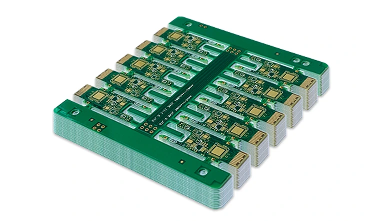
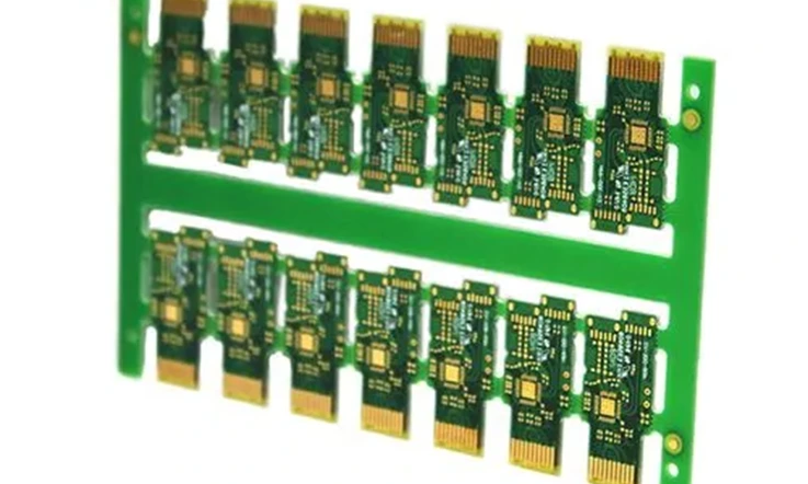
What Are Gold Fingers?
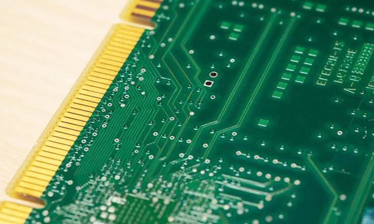
Gold fingers are the shiny, gold-plated edges found on printed circuit boards (PCBs) that facilitate connections to other devices or connectors. These connectors act as the handshake between various electronic components, ensuring a seamless interaction that enhances overall functionality. When a PCB is mated with a corresponding connector, these gold fingers create reliable electrical contact, allowing signals and power to flow efficiently.
Gold plating on these connectors serves multiple purposes. First, it greatly improves signal integrity by minimizing the electrical resistance at the contact points. This characteristic is especially beneficial in applications involving high-frequency signals, where even the slightest interference can lead to performance degradation. For instance, in high-speed data transmission, having gold-plated contacts helps maintain clarity and stability in communication, making them indispensable in consumer electronics like smartphones and computers.
Moreover, gold fingers contribute to the longevity of the connections. Gold is highly resistant to oxidation and corrosion, ensuring that the connectors remain functional over time, even in challenging environments. In scenarios such as military or aerospace applications, where durability is paramount, the presence of gold plating helps prevent failures that could arise from environmental factors. This means that devices can operate reliably without frequent maintenance or replacement.
The design of gold fingers is also a consideration during the PCB manufacturing process. Their length, thickness, and plating method are tailored to meet specific application needs. For example, edge connectors used in modular systems often require gold fingers that can withstand repeated insertion and removal cycles. By employing hard gold plating techniques, manufacturers can enhance the wear resistance of these connectors, allowing them to endure the rigors of everyday use.
In addition, The quality of the gold plating has a direct impact on performance, durability, and cost. That’s why it’s essential for engineers and manufacturers to pick the right thickness for their applications. Imagine a gaming console where rapid signal processing is vital. The integrity of these gold fingers ensures that data flows smoothly and efficiently, keeping users happy and engaged.
Importance of Gold Finger PCB Plating Thickness
When it comes to Gold Finger PCB Plating Thickness, you can’t afford to overlook its importance. Here’s why thickness matters:
Wear and Corrosion Resistance: Thicker gold plating ups the ante on wear and corrosion resistance. In high-cycle applications—where connectors are plugged and unplugged repeatedly—this thickness makes all the difference. For instance, military-grade equipment, which undergoes countless insertions, benefits from thicker plating to hold up under pressure.
Longevity of Connectors: Choosing the right thickness helps extend the lifespan of connectors. This isn’t just about cutting costs; it’s about saving time and headaches down the line. Think of the hassle of replacing faulty connectors in high-end aerospace applications—nobody wants that kind of trouble!
Cost vs. Performance Balance: It’s a balancing act! While thicker plating can increase material costs, the long-term savings through reduced failures and increased durability can outweigh initial investments. So, do your homework! Pick the thickness that gives you the best bang for your buck.
Recommended Gold Plating Thickness
Gold plating thickness is not a one-size-fits-all solution. It varies based on the application:
Consumer Electronics: For most consumer devices, a gold plating thickness of 0.5 to 1.0 mils (about 12.7 to 25.4 micrometers) is the way to go. This thickness offers a good balance between conductivity and cost, perfect for devices that don’t see heavy usage.
Automotive and Aerospace Applications: When it comes to applications that demand extra durability—like automotive or aerospace—you might want to bump that thickness up to 2.0 mils (around 50.8 micrometers) or even more. The additional thickness ensures these connectors can withstand rigorous environments.
Recommended Gold Finger PCB Plating Thickness by Application
| Application | Recommended Plating Thickness (Mils) | Justification |
| Consumer Electronics | 0.5 – 1.0 | Sufficient for low-wear applications |
| Automotive | 1.0 – 2.0 | Requires durability due to vibrations and elements |
| Aerospace | 2.0 or more | High reliability needed under extreme conditions |
Therefore, grasping the ins and outs of Gold Finger PCB Plating Thickness is vital for crafting effective electronic devices. As you gear up for your next design project, keep in mind how your choices can make or break your product’s performance. Don’t just settle for the status quo—aim for excellence in your designs, and ensure those connectors are up to the task. Dive into your specifications and make informed decisions; your end-users will thank you for it!
Design Considerations for Gold Finger PCB Plating Thickness and Cost
Designing Gold Fingers for Optimal Thickness and Cost
When it comes to designing Gold Fingers, it’s not just about making them look good; it’s a whole game plan that requires careful strategizing to ensure top-notch performance. Here are a few key elements to keep in mind:
Edge Connector Positioning: The layout of edge connectors is no small potatoes. Get it right, and you’ll enhance the board’s functionality; get it wrong, and you’re asking for trouble. Keep those connectors well-positioned to ensure they hold up over time.
Anticipated Number of Connection Cycles: Think about how many times those connectors will be plugged and unplugged. If you’re designing for a gaming console, you’re looking at heavy usage. Those connectors need thicker plating to handle all that action. On the other hand, a TV remote doesn’t get much love; it can get away with thinner plating without a hitch.
Contact Pressure: It’s all about that sweet spot! You want enough pressure to ensure a solid connection, but too much could be a recipe for disaster. Consider materials that offer some cushioning to absorb any jolts and bumps.
Designing Gold Fingers is like putting together a puzzle; every piece has to fit just right. Keep these considerations in your back pocket as you draw up your plans!
PCB Layout and Finger Width Considerations
The width of your gold fingers is no trivial matter; it significantly affects both signal integrity and cost. Here’s the scoop:
Wider Fingers and Thicker Gold Plating: If you’re going wide with those fingers, you can accommodate thicker plating. This adds durability and performance, but remember, you gotta be precise to avoid shorts. Think about it this way: in high-speed digital circuits, the wider the finger, the better the signal can travel without getting bogged down.
Spacing and Cross-Talk Prevention: Don’t let your fingers get too cozy! Adequate spacing is essential to dodge cross-talk—the last thing you want is signals stepping on each other’s toes. Aim for at least 1.5 times the width of the fingers for spacing to keep those signals flowing cleanly.
Cost Implications: Remember, bigger isn’t always better! While wider fingers and thicker plating can boost performance, they’ll also crank up manufacturing costs. Strike a balance—make sure your designs are not just effective but also wallet-friendly.
Design Considerations for Gold Finger Width and Thickness
| Consideration | Impact on Performance | Recommended Practices |
| Finger Width | Affects resistance and signal integrity | Wider fingers improve durability but require careful application |
| Spacing | Prevents cross-talk and enhances signal quality | Minimum spacing of 1.5x the finger width |
| Thickness of Plating | Increases wear resistance and longevity | Thicker plating for high-use applications |
In a nutshell, nailing the design of Gold Fingers requires a thoughtful approach. By considering edge connector positioning, connection cycles, contact pressure, finger width, and spacing, you can create PCBs that not only perform like champs but also keep costs in check. So, before you dive into your next project, keep your game face on and remember: a solid design is your ticket to success! Stay sharp and make those connections count!
Quality Control in Gold Finger PCB Plating
Quality control is where the rubber meets the road when it comes to ensuring that Gold Finger PCBs not only look good but perform like champs. From adhesion tests to inspecting plating uniformity, every step in this process plays a role in delivering a product that can handle the heat. Let’s break it down!
Adhesion and Pull Testing for Durability
To make sure that the gold plating sticks like it should, manufacturers perform adhesion tests. This isn’t just a formality—it’s about ensuring that the plating will hold its own under real-world conditions without peeling off. We’re talking about connectors that need to be as tough as nails.
Pull testing is one of the go-to methods used to measure adhesion strength. During this test, a specific force is applied to the plating to check how well it clings to the substrate. A strong adhesion process is a game plan for ensuring that the plating won’t bail when it’s needed most. This is especially true for high-reliability applications, like aerospace or medical devices, where failure is simply not an option.
Example: Pull Testing in Action
Imagine a connector in an airplane’s navigation system. If it fails due to poor adhesion, it could be lights out for safety. That’s why manufacturers may conduct pull tests that simulate extreme conditions, ensuring their products can withstand the rigors of the skies.
Inspection of Plating Uniformity
Uniformity in plating thickness is another critical aspect of quality control. Automated inspection systems are the secret sauce here; they can spot inconsistencies that the naked eye might miss. These systems use cutting-edge imaging techniques to check the gold layer’s uniformity across the PCB.
A consistent gold layer isn’t just about appearances; it packs a punch when it comes to signal integrity and durability. When the thickness is even, the electrical properties remain stable, reducing the risk of failures caused by thin spots or excess thickness.
Importance of Plating Uniformity
| Aspect | Impact | Recommended Action |
| Thickness Variation | Can lead to signal loss or failure | Implement automated inspection systems |
| Uniform Layer | Ensures consistent performance | Conduct regular calibration of inspection tools |
| Detecting Inconsistencies | Prevents costly production errors | Use advanced imaging techniques |
Wear Resistance Testing
Next up is wear resistance testing, which simulates real-world usage by performing repeated insertions and removals. This test is a real eye-opener; it helps determine how long the gold plating can hold its own under specific conditions, allowing engineers to make informed decisions about the right plating thickness.
By putting connectors through their paces, manufacturers can get a good read on wear patterns and spot potential weaknesses before they rear their ugly heads. This kind of testing gives engineers peace of mind, knowing they’re delivering a product that’s built to last.
Real-World Application
Take consumer electronics, for example. Connectors in a gaming console are used multiple times a day. A robust wear resistance test can show how well the gold plating holds up after hundreds or thousands of cycles. This ensures that connectors not only perform but also maintain their integrity throughout their lifespan.
In a word, quality control in Gold Finger PCB plating is not just a step in the process; it’s the foundation that ensures reliability and performance. By zeroing in on adhesion tests, inspecting plating uniformity, and conducting wear resistance tests, manufacturers can deliver products that meet the highest standards.
So as you gear up for your next PCB project, keep this in mind: paying attention to quality control can make all the difference between just another board and a top-tier performer. Don’t skimp on the details—make sure your Gold Fingers are ready to rock!
How to Choose the Right Plating Process for Your Gold Finger PCB
Choosing the right plating process for your Gold Finger PCB doesn’t have to be a daunting task. By understanding the characteristics of each option and aligning them with your project’s requirements, you can navigate this decision with confidence. Whether you opt for the robust qualities of electroplating or the efficient approach of immersion gold, ensuring that your PCB meets performance expectations will pay off in the long run. So, roll up your sleeves and dive into the details to make the best choice for your next project!
Electroplating vs. Immersion Gold: Which Should You Choose?
When it comes to plating methods, electroplating and immersion gold are the big players in the field, each bringing unique benefits to the table.
Electroplating is like the classic rock of plating processes—it’s cost-effective and widely used across various industries. However, it’s not all sunshine and rainbows. This method can lead to uneven thickness if the process isn’t monitored closely, which might lead to issues down the line, particularly in high-performance applications.
On the flip side, immersion gold is like a well-crafted gourmet dish: it offers superior uniformity and excellent electrical properties, making it ideal for high-frequency applications. But it does come with a steeper price tag, so you’ll want to consider your budget before diving in.
Comparison of Plating Processes
| Plating Method | Advantages | Drawbacks |
| Electroplating | Cost-effective, widely available | May yield uneven thickness, requires close monitoring |
| Immersion Gold | Superior uniformity, great for high-frequency applications | Higher cost, may require additional processing time |
Benefits and Drawbacks of Electroplating
Electroplating remains a popular choice due to its affordability and accessibility, especially for projects that don’t require the highest level of precision. Here’s the lowdown:
Benefits:
Cost-Effectiveness: For manufacturers on a budget, electroplating can save a pretty penny without compromising too much on quality. It’s like getting a good deal on a solid used car; it may not be the flashiest, but it gets the job done.
Availability: This method is widely used and readily available, making it easier to find a manufacturer who can accommodate your needs.
Drawbacks:
Inconsistencies in Thickness: The main hiccup with electroplating is the potential for uneven plating. This inconsistency can lead to a range of problems, particularly in high-reliability applications where even a minor flaw can spell trouble.
Monitoring Requirements: Industries that demand precise specifications—like telecommunications or aerospace—need to keep a watchful eye on the electroplating process. This means investing in quality control measures to mitigate risks.
Real-World Application
Consider a consumer electronics manufacturer producing a new line of smartphones. They might opt for electroplating due to the cost savings, but they must also implement stringent quality checks to ensure the connectors hold up under regular use. Regular pull tests and inspections can help ensure the product’s longevity.
Cost Impact of Thicker Gold Plating on Gold Finger PCBs
When you’re diving into Gold Finger PCB Plating Cost, you’ll quickly find that the thickness of the gold plating can really shake things up financially. Let’s break down how adding a little extra thickness can influence your bottom line and why it’s worth every penny.
Does Increasing Gold Finger PCB Plating Thickness Raise Costs?
You bet it does! Boosting the Gold Finger PCB Plating Thickness means you’ll be shelling out more dough. Here’s the lowdown:
Material Costs: The more gold you slap on, the heftier your bill will be. Gold’s not just shiny; it’s pricey, and when the market does its dance, so does your budget. For instance, if gold prices surge, manufacturers will definitely feel the heat.
Production Process: Let’s be real—thicker plating might require a few extra steps in the production line, which can also hike up labor costs. Think of it this way: you’re not just buying gold; you’re investing in a process. Specialized tools and longer processing times come into play, and those costs can add up faster than you can say “gold-plated.”
Long-Term Investment: But don’t sweat it too much! This isn’t just about today’s wallet. In high-stakes settings—like aerospace or military applications—going for thicker plating is a no-brainer. It cuts down on headaches down the road, meaning fewer repairs and lower maintenance costs.
Example of Cost Analysis
Imagine you’re rolling out two types of Gold Finger PCBs for different gigs: a consumer gadget and a medical device.
●Thickness: 1 mil
●Material Cost: $0.05 per unit
●Expected Lifecycle Cost: $1.00 over 3 years due to replacements.
●Thickness: 2 mils
●Material Cost: $0.15 per unit
●Expected Lifecycle Cost: $0.50 over 5 years due to reduced failures.
This scenario shows that while the upfront costs for the medical device PCB might be higher, you’re laughing all the way to the bank with those long-term savings.
ROI Considerations for Thicker Gold Finger PCB Plating
Now let’s talk ROI. Sure, thinner gold plating might seem like the smart choice for your wallet upfront, but hold your horses! Early failures can hit you hard with replacements and repairs, especially in industries where quality is king. Thicker plating can often lead to greater durability and a longer lifespan for your gear.
Durability Over Time: Choosing thicker plating isn’t just about being fancy. It’s about keeping your connections solid for the long haul. Sure, thinner might look cheaper now, but it could lead to costly headaches later. Thicker plating tends to hold up better against wear and tear, making it a wise choice for applications that can’t afford any hiccups.
Industry Examples: Take the automotive sector, for instance. They face some rough conditions, and investing in thicker plating can save you a world of trouble down the line. The extra cost upfront? Totally worth it when you’re avoiding failures that could cause major downtime.
Lifecycle Cost Analysis: Don’t just look at what you’re spending now; think long-term. A lifecycle cost analysis (LCCA) can really open your eyes to the financial implications of plating thickness. Make sure you’re factoring in not just manufacturing costs but also potential future failures and the costs tied to maintenance and replacements over your product’s life.
Cost Impact Analysis of Gold Finger PCB Plating Thickness
| Plating Thickness | Material Cost per Unit | Lifecycle Cost | Estimated Lifespan | Risk of Failure |
| 1 mil | $0.05 | $1.00 | 3 years | High |
| 2 mil | $0.15 | $0.50 | 5 years | Low |
Final thoughts, the thickness of gold plating on Gold Finger PCBs can swing your costs in either direction, depending on how you play your cards. While thicker plating might hit you in the pocket at first, think of it as a smart investment for the long haul. If you’re in a high-reliability field, keeping an eye on the cost impact of plating thickness isn’t just smart—it’s a savvy move!
So, gear up, weigh your options, and make the choice that best fits your needs. Don’t hesitate to reach out if you’ve got questions or want to dive deeper into the specifics!
Wrapping Up
In the end, selecting the right Gold Finger PCB Plating Thickness while managing costs is not just a decision—it’s a strategic play that can make or break your project. It all boils down to understanding the specific needs of your application, your budget constraints, and the long-term reliability of the final product. For consumer electronics, opting for thinner plating might fit the bill nicely and keep your costs in check. But when you’re stepping into high-reliability industries—think medical devices, aerospace, or military applications—going for thicker plating often becomes the smarter bet.
The Balancing Act: Durability, Cost, and Performance
By digging deep into how plating thickness impacts durability, cost, and overall performance, you’re setting yourself up to make decisions that benefit both your product’s lifecycle and your bottom line. Here are some key points to keep in mind:
Application Frequency: Ask yourself, how often will these connectors be put to the test? If they’re going to be in the trenches—frequently engaged and disengaged—you’ll want that thicker gold plating to ensure longevity and reliability. For example, connectors in a gaming console may face hundreds of insertions every day, which clearly calls for a robust solution.
Wear and Tear Consideration: What level of wear will these connectors endure? Consider a scenario where connectors are exposed to extreme environments or conditions, such as temperature fluctuations or moisture. Thicker plating can provide the resilience needed to weather these challenges.
Cost of Failure: Let’s face it—what’s the cost of failure? The last thing you want is to have your product fall flat due to unreliable connections. In high-stakes applications, the cost of a failure can skyrocket, not just in terms of repairs but also in reputational damage. A robust design can save you from a world of hurt.
Are you ready to elevate your Gold Finger PCB designs? Whether you’re an engineer refining your specifications or a procurement specialist navigating costs, our expert team is here to help. Contact us today to schedule a consultation and discuss how we can optimize your PCB design for durability and cost-effectiveness. Let’s work together to make your next PCB a standout performer!
FAQ Section
What is the ideal gold plating thickness for Gold Finger PCBs?
The ideal thickness typically ranges from 0.5 to 1.0 mils (12.7 to 25.4 micrometers) for consumer electronics, while high-reliability applications may require 2.0 mils (50.8 micrometers) or more.
How does gold plating thickness affect cost?
Thicker gold plating increases material and processing costs, necessitating careful consideration to balance thickness with expected durability and budget constraints.
Can thinner gold plating suffice for high-frequency applications?
Thinner plating may work, but it’s critical to assess the specific demands of your design. High-frequency applications usually benefit from thicker plating for optimal conductivity and signal integrity.
What factors should I consider when selecting a plating method?
Consider application requirements, cost constraints, durability needs, and operating environment. Electroplating is often more economical, while immersion gold provides better uniformity.
How can I ensure quality in gold plating?
Implement rigorous quality checks, including adhesion and wear resistance testing. Collaborate with your plating supplier to establish clear quality standards and expectations.


