
Gold finger PCBs are widely utilized in electronic devices thanks to their dependable electrical connections and compact design. The layout of the PCB stackup—the arrangement and composition of its layers—greatly influences the board’s electrical performance, signal integrity, and overall reliability.
Think of gold finger PCBs as the hidden champions of modern electronic design, linking various components effortlessly and keeping everything on track Knowing how to effectively layout a gold finger PCB stackup is a must for any PCB designer looking to create high-performance products.
For example, consider how a well-designed gold finger layout can prevent signal loss in a high-speed communication device, allowing data to flow like a breeze. So, whether you’re a seasoned pro or just starting out, let’s roll up our sleeves and explore the ins and outs of gold finger stackups. Don’t hesitate to grab a notepad—this is going to be packed with tips that can really level up your designs! In this article, we’ll dive deep into the nitty-gritty of gold finger layouts, offering insights tailored for PCB design engineers, electronics manufacturers, and newcomers alike.
Understanding Gold Finger PCB Designs
Definition and Purpose of Gold Fingers
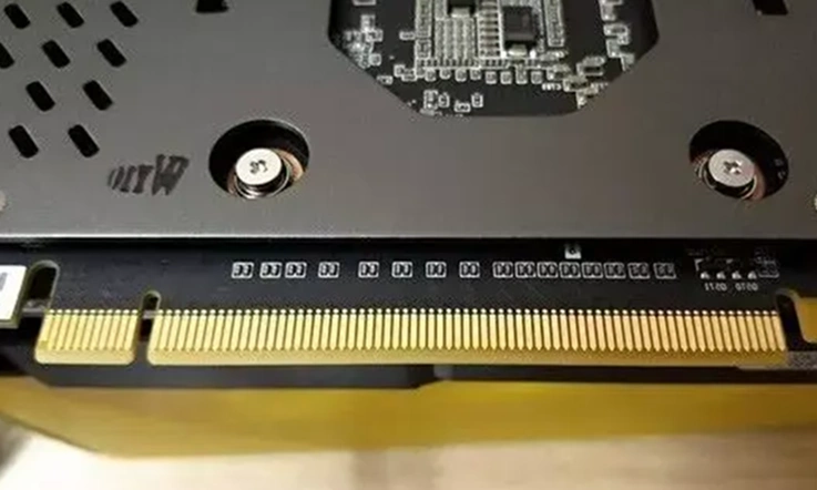
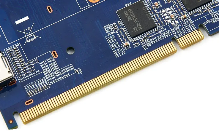
Gold fingers are the gold-plated pads located on the edges of printed circuit boards (PCBs), serving as vital connectors to other boards or components. Their main purpose is to ensure reliable electrical connections, especially in high-speed applications where timing is everything.
Role of Gold Fingers in High-Speed Applications
In the fast-paced world of electronics, speed rules the game. Gold fingers shine here by reducing signal loss and enhancing data integrity, which is key for devices operating at high frequencies. For instance, if you’re working on a high-frequency communication device, poor gold finger design could lead to data hiccups and dropped signals—definitely not what you want!
| Application | Impact of Gold Fingers |
| High-Frequency Devices | Minimize signal loss, enhance integrity |
| Consumer Electronics | Ensure seamless communication |
| Industrial Systems | Provide durability and reliability |
Benefits of Using Gold Fingers in PCB Applications
Gold fingers not only enhance electrical connectivity but also provide impressive durability against corrosion and wear. They’re a top pick in a variety of applications, from consumer electronics to complex industrial setups. Plus, gold’s natural resistance to oxidation helps keep those connections stable over time, slashing maintenance costs and boosting device reliability.
Example: Performance in Consumer Electronics
Consider a smartphone—gold fingers ensure seamless communication between the device’s components. When you tap your screen, those gold fingers are hard at work, making sure your commands are transmitted without a hitch.
If you want to take your PCB designs to the next level, think about incorporating gold fingers into your stackup. It’s a smart move that can significantly improve your product’s performance and longevity. So, gear up and start discovering the benefits of gold fingers today!
Significance of Layout Stackup
Why Layout Stackup Matters for Gold Finger PCBs?
A well-structured stackup is key to maximizing the performance of gold finger PCBs. The arrangement of layers directly influences signal integrity and overall board functionality. Think of the stackup as the foundation of a house—if it’s not solid, everything built on top can come crashing down.
Impact on Signal Integrity and Performance
Proper layout stackup minimizes electromagnetic interference (EMI) and helps maintain the necessary impedance levels for high-speed signals. For example, a well-designed stackup ensures that high-speed signals travel smoothly without reflections, keeping data transmission crystal clear.
| Stackup Factor | Impact on Performance |
| Layer Arrangement | Affects signal path and integrity |
| Controlled Impedance | Reduces reflections and enhances stability |
| EMI Minimization | Prevents noise and enhances signal clarity |
Enhancing Reliability through Proper Stackup Design
By thoughtfully designing the stackup, you can boost the reliability of your gold finger PCB. This not only extends the product’s lifespan but also cuts down on the chances of costly errors during production. For instance, using multilayer stackups with controlled impedance can significantly improve performance in applications like automotive electronics, where reliability is non-negotiable.
Example: Automotive Electronics
Consider an automotive system that relies on real-time data. A well-designed stackup can mean the difference between smooth operation and a system failure on the road. Keeping everything running without a hitch is what it’s all about!
If you’re ready to take your PCB designs up a notch, don’t underestimate the power of a solid layout stackup. Dive into the details and make informed decisions that will elevate your designs and improve performance across the board. Now’s the time to dive in and get started!
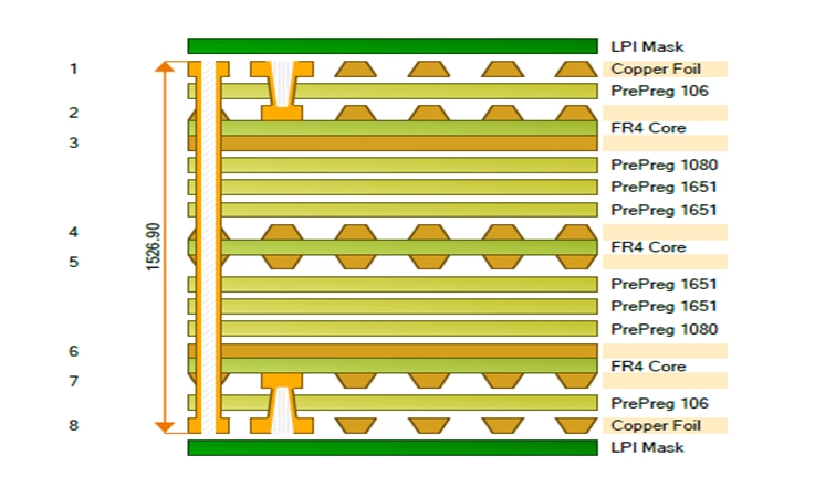
Stackup Architecture of PCB Gold Fingers
Layer Arrangement for Optimal Performance
When designing a gold finger PCB stackup, it’s essential to think carefully about the arrangement of the layers. Each layer plays a vital role in the overall performance and effectiveness of the board. Imagine the layers working together like a well-rehearsed band—each one needs to hit the right notes to create a harmonious performance.
Multi-layer PCB Design Fundamentals
Multi-layer designs open up a world of possibilities for creating more complex circuits, allowing for higher density connections without sacrificing performance. For instance, using a 4-layer stackup provides ample routing space for signals while keeping the design compact. Careful planning is key to optimizing these multilayer configurations for gold finger applications.
| Layer Count | Advantages |
| 2-Layer | Simple designs, cost-effective |
| 4-Layer | Good balance of space and complexity |
| 6-Layer or More | Supports high-density circuits, advanced performance |
Impedance Control in Gold Finger Stackup
Keeping impedance in check is essential, especially for high-speed signals. A well-designed stackup can prevent reflections and signal degradation, ensuring that your connections remain solid. Techniques like using differential pairs and proper trace width calculations can significantly enhance impedance matching.
Example: High-Speed Communication
Consider a scenario in high-speed communication systems—getting impedance right can mean the difference between clear signals and garbled noise. When it comes to data integrity, every little detail counts!
Dive deep into the architecture of your stackup and make those layers work for you. With the right approach, you’ll not only optimize performance but also pave the way for reliable, high-speed connections. Now’s the time to dive in and design like a champ!
Key Considerations of Layout Goldfinger Circuit Board Stackup
Selecting the Right Materials for Gold Finger PCB Stackup
The materials you choose have a significant impact on the performance of your gold finger PCB. Opt for materials that boost signal integrity and thermal management. Think of it as picking the right ingredients for a recipe—using top-notch materials leads to a tastier result!
Dielectric Materials and Their Impact on Performance
Different dielectric materials provide varying levels of signal loss and thermal conductivity. For instance, using FR-4 as a substrate material strikes a solid balance between cost and performance, but if you’re looking to up your game in high-frequency applications, exploring advanced materials like Rogers or PTFE might yield better results.
| Material Type | Signal Loss | Thermal Conductivity | Ideal Use |
| FR-4 | Moderate | Good | General applications |
| Rogers | Low | Excellent | High-frequency applications |
| PTFE | Minimal | Excellent | Specialized high-speed designs |
Choosing Surface Finishes for Gold Finger Reliability
Surface finishes play a big role in ensuring reliable connections. Selecting high-quality finishes not only boosts solderability but also extends the lifespan of your gold fingers. For example, gold immersion provides excellent corrosion resistance, making it a popular choice for high-performance applications.
Initial Design Planning for Gold Finger Layout
Every successful design kicks off with a solid plan. Evaluate electrical performance criteria and thermal management needs early in the design phase to sidestep issues later on.
Evaluating Electrical Performance Criteria
Understanding your design’s electrical requirements is key. Assess voltage, current, and frequency specifications to make sure your layout meets these needs. Using simulation tools can help visualize performance under different conditions, highlighting potential bottlenecks before they become a headache.
| Performance Metric | Specification | Simulation Tool |
| Voltage | e.g., 5V | SPICE |
| Current | e.g., 2A | LTspice |
| Frequency | e.g., 1 GHz | HyperLynx |
Assessing Thermal Management Needs
Heat is the enemy of electronic components. Proper thermal management ensures your PCB operates efficiently without overheating, which can lead to failure. Implementing thermal vias and heat sinks in your design can significantly improve thermal dissipation.
Focus on selecting the right materials and planning meticulously. By paying attention to these key considerations, you’ll enhance performance and reliability in your gold finger PCBs. So get your hands dirty and start creating designs that truly stand out!
Design Software for Layout PCB Goldfinger Stackup
Recommended Design Tools for Gold Finger PCBs
Choosing the right design software is key to creating effective gold finger layouts. Several tools can streamline the design process, allowing for simulations and precise adjustments. Think of your design software as your trusty toolbox—having the right tools makes all the difference!
Features to Look for in PCB Design Software
When selecting PCB design software, look for robust simulation capabilities, intuitive interfaces, and comprehensive libraries of components. Programs like Altium Designer and OrCAD are industry favorites, known for their powerful features and user-friendly experiences. These tools can help you design with confidence and precision.
| Software | Key Features | Ideal For |
| Altium Designer | Advanced simulation, intuitive UI | Complex designs |
| OrCAD | Comprehensive library, ease of use | Beginners to advanced users |
| KiCAD | Open-source, flexible options | Budget-conscious designers |
Integrating Simulation Tools in the Design Process
Using simulation tools can help predict how your design will behave under different conditions. This proactive approach can save time and resources, ensuring that your layout is as efficient as possible. For example, utilizing tools like ANSYS or HyperLynx for signal integrity simulations can provide valuable insights that prevent headaches later on.
Example: Signal Integrity Simulations
Imagine you’re working on a high-speed communication device. Running simulations can reveal potential issues before you even hit the prototype stage. It’s like having a crystal ball that lets you see and fix problems ahead of time!
Invest some time in finding the right design software and integrating simulation tools into your process. With the right resources at your fingertips, you’ll create gold finger PCBs that stand the test of time. Now’s your chance to make designs that really pack a punch!
Step-by-Step Guide to Layout a Gold Finger PCB Stackup
1. Techniques for Effective Layout of Gold Finger PCBs
To ensure your gold finger connections are reliable, follow best practices for layout and component placement. Consistency in design leads to more dependable products. For instance, maintaining uniform pad sizes and ensuring proper alignment during assembly can help prevent common manufacturing defects. Think of it like setting a solid foundation before building a house—everything rests on it!
| Technique | Description | Benefits |
| Uniform Pad Sizes | Keep pad sizes consistent across the design | Reduces assembly errors |
| Proper Alignment | Ensure all components align perfectly | Enhances connection reliability |
| Layer Stackup Planning | Plan your layer arrangement meticulously | Optimizes signal integrity |
2. Quality Control Measures in Gold Finger Manufacturing
Quality control should always be front and center in your design process. Implementing rigorous testing and validation procedures can safeguard your design’s integrity. For example, employing techniques like Automated Optical Inspection (AOI) helps catch defects early in the manufacturing process. This proactive approach can save time and money down the line, ensuring that your product is ready to hit the market without a hitch.
Example: Using AOI in Manufacturing
Imagine you’re ramping up production for a new electronic device. By incorporating AOI, you can spot misalignments and soldering issues before they become costly problems. It’s like having a safety net that keeps your design on track!
Follow these techniques and incorporate quality control measures from the get-go. By prioritizing reliability and quality, you’ll be well on your way to producing outstanding electronic products. Don’t just aim for good—strive for great!
Common Challenges in Layout of Gold Finger PCB Designs
Identifying Potential Issues in Gold Finger Layout
Every design process comes with its share of bumps in the road. Identifying potential issues early can save you time and resources down the line. Common challenges include improper alignment of gold fingers and inadequate signal integrity stemming from subpar stackup design. Think of it as spotting a flat tire before you hit the highway—better safe than sorry!
| Common Issue | Description | Impact |
| Improper Gold Finger Alignment | Misalignment during manufacturing | Causes connection failures |
| Poor Stackup Design | Inadequate layer arrangement | Leads to signal degradation |
| Insufficient Ground Planes | Lack of grounding can increase noise | Impacts overall performance |
Solutions for Optimal Gold Finger PCB Stackup Performance
Advanced Manufacturing Techniques for Gold Fingers
Staying current with advanced manufacturing techniques can really enhance the performance and reliability of your gold finger PCBs. Explore innovative methods like Laser Direct Structuring (LDS), which can boost efficiency and offer greater design flexibility. It’s like upgrading from a flip phone to a smartphone—game-changing!
Design Adjustments for Enhanced Signal Integrity
Sometimes, making a small tweak can lead to big payoffs. Regularly revisit your design parameters to ensure optimal performance. Techniques such as adding ground planes or using via stitching can significantly help maintain signal integrity. These adjustments may seem minor, but they can make a world of difference in your final product.
By identifying potential issues early and applying innovative solutions, you’ll set yourself up for success. Don’t just go through the motions—get proactive about your design process and watch your projects thrive!
Applications and Case Studies of Gold Finger PCB Stackup
Real-World Implementations of Gold Finger PCB Layouts
Examining real-world applications offers a treasure trove of insights into best practices and common pitfalls. Learning from the successes and challenges faced by others can serve as your guiding light in the design process. It’s like having a mentor who’s been around the block a few times—super valuable!
| Industry | Application | Key Benefits |
| Consumer Electronics | Smartphones | Reliable connections for seamless data transmission |
| Telecommunications | Network Equipment | Ensures uninterrupted service |
| Automotive | Advanced Driver Assistance Systems (ADAS) | Enhances safety features and reliability |
Performance Optimization in Consumer Electronics
Gold fingers are a staple in consumer electronics, providing the reliable connections that power our everyday gadgets. Take smartphones, for example—these devices often utilize gold fingers for their connectivity modules, ensuring smooth data transmission. It’s like the glue that holds everything together, keeping your apps running smoothly!
Applications in Telecommunications and Other Industries
Beyond consumer electronics, gold fingers shine in telecommunications, automotive, and industrial applications, showcasing their versatility and reliability. In telecommunications, gold fingers facilitate connections in network equipment, ensuring that services run without a hitch. Picture a busy office relying on stable internet—gold fingers are the unsung heroes behind the scenes!
Lessons Learned from Successful Gold Finger Projects
Every project has its nuggets of wisdom. Reflecting on past experiences can inform your future designs and elevate your expertise in PCB layout. For instance, a project that initially struggled with signal integrity might prompt the adoption of better impedance control measures in future designs. Remember, it’s not about falling down; it’s about how you get back up and improve!
By exploring real-world applications and learning from case studies, you’ll arm yourself with the knowledge needed to create stellar designs. Don’t just stand on the sidelines—get your hands dirty and start optimizing your projects today!
Future Trends in Gold Finger PCB Layout Technology
Innovations on the Horizon for Gold Finger Designs
The PCB landscape is continually evolving, and keeping your finger on the pulse of the latest trends is key to staying ahead of the game. Emerging technologies, such as flexible PCBs and integrated circuit packaging, are paving the way for new applications of gold fingers. For instance, flexible PCBs can bend and twist without compromising performance, making them ideal for modern wearable technology.
| Emerging Technology | Application | Benefits |
| Flexible PCBs | Wearable Devices | Lightweight, adaptable design |
| Integrated Circuit Packaging | Compact Electronics | Reduces space while enhancing performance |
Preparing for Evolving Challenges in Gold Finger PCB Layout
As technology marches on, new challenges will inevitably arise. Anticipating these shifts will keep your designs relevant and effective in a fast-paced industry. Staying informed through industry publications and attending conferences can provide valuable insights into future trends. Think of it as being part of a community that’s always sharing the latest and greatest—don’t miss out!
Are you ready to embrace the future of gold finger PCBs? By staying ahead of the curve and exploring emerging technologies, you’ll be well-equipped to tackle the challenges that lie ahead. Dive into industry resources and network with peers—your next big idea could be just around the corner!
Finial Thoughts
In this article, we dived into the nuts and bolts of effectively laying out a gold finger PCB stackup. We discussed the significance of layout stackup, material selection, and the impact on signal integrity, as well as explored real-world applications. Grasping these elements is key for crafting efficient and reliable circuit boards.
Now, it’s your turn to roll up your sleeves! Whether you’re a seasoned PCB design engineer or just starting out, these principles can seriously boost your design process. Why not take the plunge and start designing your next gold finger PCB layout? Don’t forget to share your experiences and best practices with your crew!
If you’ve got more questions or insights about gold finger PCBs, drop a comment below or connect with industry experts. Let’s push the limits of design together!
Frequently Asked Questions (FAQs) about Gold Finger PCB Layout
1. What are gold fingers, and why are they used in PCBs?
Gold fingers are gold-plated pads located at the edges of PCBs that facilitate connections to other boards or components. They are used because they provide reliable electrical connections, especially in high-speed applications where maintaining signal integrity is vital.
2. How does the stackup configuration affect gold finger performance?
The stackup configuration plays a significant role in the performance of gold finger PCBs. Proper layer arrangement minimizes electromagnetic interference (EMI) and helps maintain the necessary impedance levels, which is essential for high-speed signal transmission. A well-planned stackup ensures that high-speed signals travel smoothly without reflections.
3. What materials are best for gold finger PCB stackup?
Choosing the right materials is critical for optimal performance. For standard applications, FR-4 is a popular choice due to its balance of cost and performance. For high-frequency applications, advanced materials like Rogers or PTFE may be better suited as they offer lower signal loss and improved thermal management.
4. What are some common challenges when designing gold finger PCBs?
Common challenges include ensuring proper alignment of gold fingers, maintaining signal integrity through appropriate stackup design, and selecting suitable surface finishes. Early identification of these issues can prevent costly errors down the road.
5. How can I improve the reliability of my gold finger PCB connections?
To enhance the reliability of gold finger connections, it’s essential to follow best practices such as maintaining uniform pad sizes, ensuring proper alignment during assembly, and selecting high-quality surface finishes. Regular quality control checks during manufacturing also help catch defects early.
6. What software is recommended for designing gold finger PCBs?
Several design tools are available that cater to gold finger PCB layouts, such as Altium Designer and OrCAD. These programs offer robust simulation capabilities and comprehensive libraries, making them ideal for ensuring your designs meet all necessary performance criteria.


