
Designing a Goldfinger PCB is akin to crafting a fine piece of machinery. Every detail matters, and a well-thought-out design can be the difference between a successful product and one that doesn’t meet expectations. In this guide, we’ll explore the nuances of Goldfinger PCB design, focusing on the principles, materials, manufacturing processes, and best practices that can elevate your project.
The Fundamentals of Goldfinger PCB Design
What is a Goldfinger PCB?
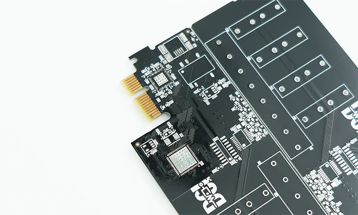
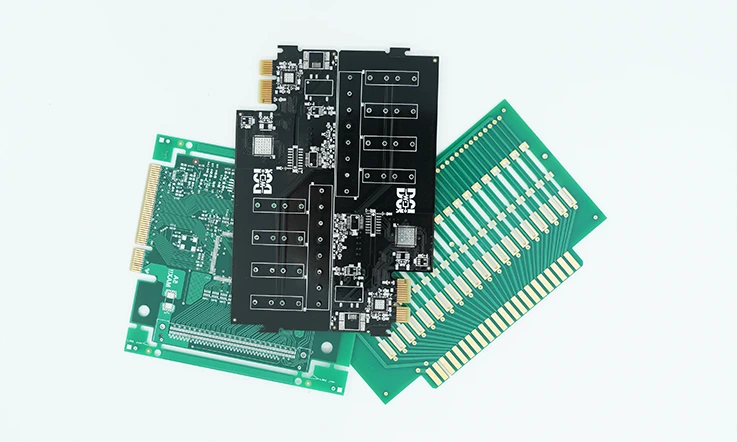
A Goldfinger PCB features gold-plated edges that serve as connection points for edge connectors. These gold fingers enhance conductivity and provide durability, making them ideal for applications in telecommunications and consumer electronics.
The Role of Design in PCB Development
When delving into Goldfinger PCB design, understanding that the design phase goes beyond creating a layout is essential. It’s about strategizing for the entire product lifecycle. The decisions made here will resonate throughout manufacturing and beyond.
Key Design Parameters
Material Selection: Choosing the right substrate—like FR-4 or Rogers—can influence thermal performance and signal integrity. A solid material choice is akin to selecting the right canvas for a masterpiece.
Gold Plating Thickness: The thickness of the gold is another key aspect. You want enough to ensure durability without overspending. Typically, 0.5 to 2.5 microns hits the mark, but this can vary based on application.
Key Design Considerations for Goldfinger PCBs Board
When embarking on the journey of designing a Goldfinger PCB, several key considerations will steer you in the right direction.
Types of Gold Fingers
Understanding the various types of gold fingers is paramount. These can range from standard designs, which are widely used, to custom solutions tailored for specific applications.
Standard vs. Custom Designs: Standard gold finger designs are often used in mass production, ensuring efficiency and cost-effectiveness. On the flip side, custom designs allow for greater flexibility and can be tailored to unique requirements, providing a perfect fit for specialized applications.
Edge Connectors Explained
Edge connectors are the lifeblood of Goldfinger PCBs, providing the means for electrical connections. These connectors allow for easy insertion and removal, making them ideal for devices that require regular maintenance or upgrades.
Electrical Connections and Reliability
Reliability is key when it comes to electrical connections. A poorly designed PCB can lead to intermittent failures and reduced performance.
Ensuring Electrical Performance: When designing your PCB, consider factors such as trace width, spacing, and material selection. These elements play a significant role in the overall performance of your Goldfinger PCB.
Factors Influencing Reliability
Environmental factors such as temperature, humidity, and mechanical stress can affect the reliability of your PCB. Designing with these factors in mind can help ensure longevity and optimal performance.
PCB Gold Finger Bevel Edge Design
One critical aspect of Goldfinger PCB design is beveling the edges. This technique is more than just a design choice; it significantly enhances the functionality and durability of the board.
Importance of Beveling
Beveling the edges of your PCB can enhance its mechanical strength and reduce the risk of damage during insertion into connectors.
Enhancing Mechanical Strength: A well-executed bevel design will help distribute stress more evenly across the edge of the PCB, minimizing the risk of cracking or chipping.
Design Techniques for Effective Beveling
When it comes to beveling, precision is key. Utilizing the right tools and techniques can make all the difference. CNC milling is often employed for its accuracy, ensuring a perfect edge every time.
Design Considerations: The bevel angle typically ranges from 30 to 45 degrees. This angle enhances aesthetics and reduces the risk of chipping during insertion and extraction.
Manufacturing Techniques: Precision in bevel edge design is essential. CNC machining or laser cutting can ensure smooth, uniform edges, contributing to better contact reliability.
Impact on Performance: The beveled design helps minimize stress concentrations that could lead to failures over time, ensuring edges fit seamlessly with connectors.
Case Studies: Overcoming Design Challenges
Case Study 1: Telecommunications Device
Background: A telecommunications company aimed to develop a high-speed data transfer module using Goldfinger PCBs. The initial design faced significant challenges related to signal integrity, particularly with crosstalk and attenuation.
Challenge: The design team discovered that the inadequate grounding and trace layout were contributing to over 30% signal loss.
Solution:
Redesign of Ground Plane: Integrated a solid ground plane and increased the via count.
Trace Width Adjustment: Recalibrated trace widths based on IPC-2221 guidelines.
Outcome: Testing revealed a 40% improvement in signal integrity, enhancing overall performance.
Case Study 2: Consumer Electronics
Background: A consumer electronics manufacturer produced gaming consoles that required robust Goldfinger connections.
Challenge: Gold fingers experienced wear due to repetitive insertion and extraction.
Solution:
Beveled Edge Implementation: Introduced bevel edge design to reduce stress.
Enhanced Gold Plating: Opted for a gold plating thickness of 3 microns.
Outcome: Noted a 25% decrease in warranty claims and a significant increase in customer satisfaction.
Case Study 3: Medical Device
Background: A medical device manufacturer was developing a portable diagnostic tool that utilized Goldfinger PCBs.
Challenge: The compact design led to overheating issues.
Solution:
Thermal Management Strategies: Implemented thermal vias and heat sinks.
Signal Integrity Analysis: Used simulation tools to analyze signal behavior.
Outcome: Successfully passed regulatory tests with improved thermal performance, meeting market demands.
PCB Gold Finger Plated Gold Thickness Design
The thickness of the gold plating on your PCB’s gold fingers is another essential factor to consider.
Gold Thickness Specifications: Gold thickness plays a crucial role in determining the performance and durability of your Goldfinger PCB.
Impact on Performance and Cost: While thicker gold plating can enhance electrical conductivity and reduce wear, it can also drive up costs. Striking a balance between performance and budget is essential.
Industry Standards and Recommendations: Staying updated with industry standards for gold plating thickness can help you make informed decisions during the design process, ensuring compliance and optimal performance.
Design Techniques for Plated Gold Finger Thickness
Standards and Specifications: Following IPC-4552 standards can guide your choice of gold thickness. For general applications, 1 to 2.5 microns is often recommended, while high-reliability uses may require 3 to 5 microns.
Electroplating vs. Electroless Plating: Both methods have advantages. Electroplating provides thicker layers at lower costs, while electroless plating offers better coverage in complex geometries.
Testing and Validation: Conducting tests like the Pull Test and Adhesion Test ensures that the gold plating meets performance criteria.
Advanced Design Techniques for Goldfinger PCBs
When it comes to Goldfinger PCBs, utilizing advanced design techniques is where manufacturers can really flex their muscles. These methods not only enhance performance but also streamline the production process, making it a win-win.
Schematic and Layout Design
Starting with a solid schematic is like laying a strong foundation for a house. Using reliable PCB design software, like Altium or Eagle, can help manufacturers translate complex ideas into tangible layouts.
Example: One manufacturer faced issues with signal integrity due to a convoluted layout. By restructuring the schematic and using appropriate layer stack-ups, they improved signal flow and reduced crosstalk significantly. It’s all about keeping it clean and straightforward.
Layer Stack-Up Considerations
The stack-up of layers in a PCB can make or break performance. Manufacturers need to consider the arrangement of layers to optimize signal integrity and thermal performance.
Signal Integrity: A well-designed ground plane is essential for minimizing electromagnetic interference, especially in high-speed applications. For instance, one manufacturer implemented a dual-layer stack-up that enhanced their product’s performance by maintaining a solid ground reference, leading to fewer signal dropouts.
Via Design: Smart via designs, like blind and buried vias, can reduce inductance and enhance signal stability. A manufacturer that integrated these vias into their design saw improved performance in high-frequency applications, proving that good design pays off.
Design Rules and Standardization
Adhering to established design rules and industry standards is a must for quality and consistency. Following IPC standards, such as:
IPC Standards: Following IPC-2221 and IPC-7351 standards ensures your designs meet industry requirements. These standards cover aspects like trace width, spacing, and via dimensions.
Design Rule Check (DRC): Regularly running DRC in your PCB design software can help identify potential issues before manufacturing, reducing costly revisions later.
Design Guidelines: Maintain a clear set of design guidelines that detail acceptable tolerances, pad sizes, and component placements. This consistency fosters quality across projects.
Example: By implementing a strict Design Rule Check (DRC) process in their design software, a manufacturer was able to catch potential issues early on, avoiding costly revisions down the line. It’s like having a safety net that keeps everything in check.
Simulation and Validation (Thermal Management Solutions)
Integrating thermal management strategies, such as thermal vias and heat sinks, ensures optimal performance in high-power applications. Conducting thermal simulations during design helps identify hot spots, guiding layout modifications for better heat dissipation.
Therefore, before production, simulating your design can save a lot of trouble. By identifying potential issues early on, you can make necessary adjustments without costly delays.
Signal Integrity Analysis: Utilize tools like HyperLynx or SIwave to analyze how signals behave in real-world conditions. This proactive approach can catch issues that manual checks might miss.
Thermal Analysis: Managing heat is vital in electronics. Conduct thermal simulations to identify hotspots and ensure your PCB can handle thermal loads effectively.
The Manufacturing Journey of Goldfinger PCBs
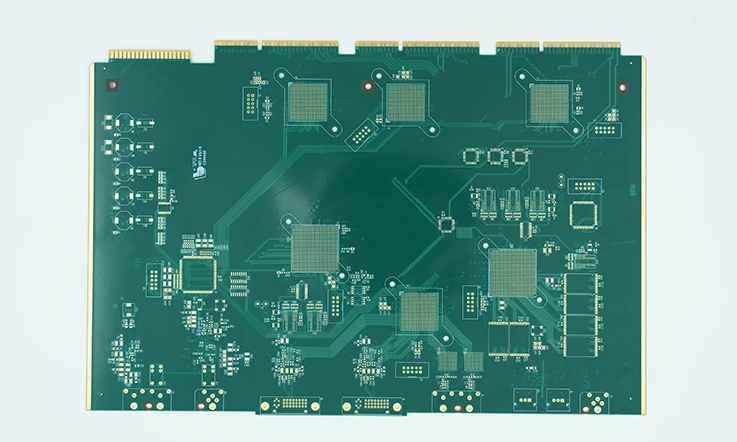
The manufacturing process of Goldfinger PCBs is a meticulous journey that involves multiple stages, each requiring precision and adherence to strict industry standards. From material selection to final inspection, every phase is integral in ensuring the performance and reliability of the final product.
Material Selection and Preparation
The journey begins with the careful selection of high-quality substrates, such as FR-4, Rogers, or specialized laminates, tailored for specific applications. The choice of substrate influences thermal management, signal integrity, and mechanical properties.
Example: For high-frequency applications, a Rogers material might be selected due to its superior dielectric properties, which help minimize signal loss.
Once selected, the substrates are processed through advanced techniques, such as laser drilling and CNC milling, to create the required layer configuration. This includes preparing the base layer with appropriate copper foil thickness—typically ranging from 1 oz/ft² to 3 oz/ft²—depending on current carrying requirements.
PCB Layer Stacking and Lamination
The next step involves layer stacking and lamination. Multi-layer Goldfinger PCBs often require precise alignment and bonding of various layers. Manufacturers utilize heat and pressure during the lamination process to ensure strong adhesion between layers, which is essential for maintaining structural integrity and electrical performance.
Example: In a 4-layer PCB, a well-designed inner layer with strategically placed power and ground planes can significantly enhance electromagnetic performance.
Gold Plating Process
Gold fingers are created through a plating process that can be either electroplated or electroless, depending on the application requirements.
Electroplating: This method is often preferred for its cost-effectiveness in producing thicker gold layers, typically between 1 to 5 microns, providing enhanced conductivity and wear resistance.
Electroless Plating: Offers superior coverage and is ideal for complex geometries where uniform gold deposition is necessary.
The choice of plating thickness is governed by the IPC-4552 standards, which guide manufacturers in selecting appropriate gold thickness for various applications, ensuring compliance with industry expectations.
Surface Finishing
Surface finishing options like ENIG (Electroless Nickel Immersion Gold) or OSP (Organic Solderability Preservative) are then applied. ENIG is favored for its excellent solderability and shelf life, making it suitable for high-reliability applications.
Example: ENIG finishes are commonly used in medical devices and aerospace applications where reliability is non-negotiable.
Quality Control and Testing
Quality assurance is paramount in Goldfinger PCB manufacturing. Advanced inspection techniques such as Automated Optical Inspection (AOI) and X-ray Inspection are employed to identify defects that could compromise performance.
Example: AOI systems can detect misaligned layers or insufficient plating thickness, allowing for immediate corrections before moving to the next phase.
Manufacturers also perform functional testing, such as electrical testing and thermal cycling tests, to validate the performance of the Goldfinger connections under real-world conditions.
Final Assembly and Packaging
After passing quality control, Goldfinger PCBs proceed to final assembly, where components are soldered onto the PCB. Manufacturers must ensure that the gold fingers are clean and free of oxidation to guarantee optimal electrical connections.
Enhancing Performance with Gold Fingers
Maximizing the performance of Goldfinger PCBs isn’t just a nice-to-have; it’s a game changer in the competitive landscape of electronics. Manufacturers have a toolkit of strategies to boost functionality while keeping costs in check.
Design Enhancements
Implementing thoughtful design enhancements can really take a Goldfinger PCB to the next level. Here are a couple of standout strategies:
Thermal Relief Pads: These pads help distribute heat evenly across the PCB, preventing those pesky hot spots that can lead to failures. When heat gets out of control, you’re looking at potential short circuits or reduced lifespan. So, make sure to incorporate thermal relief pads into your layout—it’s like giving your PCB a nice cool drink on a hot day.
Via Stitching: By adding via stitching, you can improve the return path for signals. This technique minimizes inductance and enhances signal integrity, making sure your signals don’t go haywire. Think of it as creating shortcuts in a busy city—less congestion leads to smoother traffic.
Collaboration with Manufacturers
Building solid relationships with PCB manufacturers can make all the difference. Open discussions about design needs and potential challenges can lead to smoother production processes. When manufacturers and designers are on the same page, you’re more likely to hit the sweet spot in performance and manufacturability.
Example: A manufacturer that understands the nuances of your design can suggest tweaks that enhance yield rates. If your design is a bit off the beaten path, their insights can save you time and money down the line.
Quality Control Practices
To ensure top-notch performance, robust quality control practices are a must. Employing techniques like Automated Optical Inspection (AOI) and X-ray inspection helps catch defects that could derail performance.
Example: With AOI, you can spot issues like misaligned gold fingers before they become a headache. It’s like having an eagle eye that ensures everything is on point before the PCBs head out the door.
Continuous Improvement
Manufacturers should also embrace a culture of continuous improvement. By regularly analyzing production data and incorporating feedback, companies can refine processes and enhance the overall quality of Goldfinger PCBs.
Example: If you notice a pattern of defects in a particular batch, diving into the root causes can lead to actionable insights that improve future production. It’s all about staying sharp and adaptable.
Cost Considerations in Goldfinger PCB Design
When it comes to Goldfinger PCB design, cost considerations are where the rubber meets the road. Manufacturers need to keep a keen eye on various factors that influence overall expenses while ensuring quality isn’t thrown out the window.
Material Selection
Choosing the right materials is the first step in keeping costs manageable. While high-end substrates like Rogers offer fantastic performance, they come with a price tag. Manufacturers must balance performance with budget constraints.
Example: For applications that don’t require top-shelf materials, opting for FR-4 can save a pretty penny while still delivering solid performance. It’s all about knowing when to splurge and when to save.
Manufacturing Processes
The choice between subtractive and additive manufacturing processes can significantly impact costs. Subtractive methods, though traditional, can lead to material waste if not optimized. Additive techniques might have a higher upfront cost but can reduce waste and offer flexibility for complex designs.
Example: If a manufacturer switches to additive processes for intricate components, they might find they can cut down on both material costs and production time. Talk about hitting two birds with one stone!
Gold Plating Thickness
Gold plating is a double-edged sword. While thicker plating enhances durability, it can also inflate costs. Manufacturers should consider the application and find that sweet spot in gold thickness.
Example: For consumer electronics, sticking with a plating thickness of 1 micron might do the trick, while high-reliability applications could justify going up to 3 microns. The key is to align plating choices with expected product lifecycles.
Quality Control and Testing
Investing in robust quality control measures can seem like a drain on resources initially, but it’s a smart move in the long run. Catching defects early can save a manufacturer from costly recalls and reputation hits.
Example: Implementing thorough testing protocols like X-ray inspection can help identify hidden issues before products hit the market. Think of it as an insurance policy that pays off when it counts.
Cost-Benefit Analysis
Conducting a thorough cost-benefit analysis can help manufacturers make informed decisions. Evaluating the long-term benefits of quality materials versus the immediate savings from cheaper options is key to aligning costs with product performance.
Example: If a manufacturer finds that a slightly more expensive substrate leads to a 20% reduction in failure rates, the upfront investment may just pay for itself in fewer warranty claims. It’s all about playing the long game.
The Future of Goldfinger PCB Design
As tech continues to evolve, Goldfinger PCB designs will need to keep pace. Emphasizing design finesse not only boosts performance but also streamlines production. By staying sharp and open to new techniques, designers can ensure they’re ready for whatever the future holds.
Ready to Level Up?
If you’re keen to step up your Goldfinger PCB game, remember that knowledge is power. Dive into resources, connect with fellow designers, and keep learning. The more you know, the better your designs will be.
Closing Thoughts
Goldfinger PCB design is more than just a checklist; it’s an art form that blends functionality and innovation. So roll up your sleeves and get to work—your next big project is waiting!
Wrapping Up: The Road Ahead for Goldfinger PCB Design
As technology continues to evolve, so must our approaches in Goldfinger PCB design. Emphasizing principles that prioritize both performance and manufacturability can set the stage for future innovations.
Designing a Goldfinger PCB involves crafting a reliable solution that meets the needs of today’s electronic landscape. By focusing on thoughtful design, quality materials, and strong collaboration with manufacturers, you’ll be well on your way to creating a standout product.
Ready to dive deeper into Goldfinger PCB design? Connect with industry professionals, explore resources, and keep learning. The world of PCB design is always changing, and staying ahead is key to success.
Frequently Asked Questions
What are gold fingers in PCB design?
Gold fingers are gold-plated contact points on the edges of PCBs, designed for connection with edge connectors. They enhance conductivity and durability.
How thick should gold plating be on gold fingers?
Typically, gold plating thickness ranges from 0.5 to 2.5 microns for general applications, while high-reliability uses may call for 3 to 5 microns.
Why is bevel edge design important?
Beveled edges on gold fingers reduce stress during insertion and extraction, enhancing mechanical integrity and extending connection lifespan.
What are the best practices for gold finger PCB design?
Focus on electrical performance, mechanical integrity, and manufacturability. Strive for simplicity and robust testing.


