
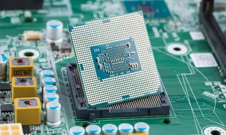
The Micro Ball Grid Array (µBGA), also known as the Micro BGA or Micro Ball Grid Array, is widely regarded as one of the most cutting-edge and sophisticated surface-mounted devices available to PCB designers. It represents a specialized subset of the general Ball Grid Array (BGA) packaging technology. In a standard BGA package, the spacing between individual balls typically ranges from 0.8mm to 1.0mm, whereas the micro BGA package exhibits a much tighter pitch of 0.4mm or even less. This significant reduction in pitch allows for a considerable decrease in package size, enabling micro BGAs to be positioned in extremely close proximity to the PCB surface.
The packaging technology employed in electronic devices plays a crucial role in their overall performance. In recent years, advancements in technology have successfully minimized the signal delay within the actual semiconductor material of integrated circuits (ICs). However, the reduction of signal delay within the IC package itself remains limited. Consequently, the package becomes an integral component in facilitating high-speed performance in electronic devices. The micro BGA, with its superior chip delay capabilities, emerges as an ideal solution among various packaging technologies available. It offers greater flexibility and efficiency compared to alternative options, allowing for enhanced performance in high-speed applications.
Advantages and applications of µBGA
Here are some common advantages and applications of µBGA (micro ball grid array) technology:
Advantages of µBGA:
Miniaturization: The small size of µBGA packages allows for high circuit density and miniaturization of electronic devices.
Increased I/O Density: The µBGA design enables a higher number of input/output (I/O) connections within a smaller footprint.
Improved Electrical Performance: The shorter electrical path lengths and reduced parasitic capacitance and inductance in µBGA packages can enhance signal integrity and electrical performance.
Enhanced Thermal Performance: The small package size of µBGA facilitates efficient heat dissipation, leading to improved thermal management.
Cost-Effective Manufacturing: The automated assembly processes for µBGA packages result in higher production yields and lower manufacturing costs compared to larger packages like BGAs or quad flat packages (QFPs).
Applications of µBGA:
Consumer Electronics: µBGA technology finds extensive use in consumer electronic devices such as smartphones, tablets, wearables, gaming consoles, and digital cameras, where space-saving and high functionality are crucial.
IoT Devices: Internet of Things (IoT) devices, including smart home devices, connected sensors, and wearable devices, often employ µBGA packages due to their compact size and low power consumption.
Automotive Electronics: µBGA packages are utilized in automotive applications, including advanced driver-assistance systems (ADAS), infotainment systems, engine control units (ECUs), and in-vehicle networking, where space constraints and reliability are important.
Medical Devices: Medical equipment, such as portable monitors, implantable devices, and diagnostic tools, can benefit from µBGA technology to achieve small form factors and high-performance requirements.
Aerospace and Defense: The aerospace and defense industries utilize µBGA packages in applications like avionics systems, satellite communications, radar systems, and military-grade electronics, where size, weight, and reliability are critical factors.
These are just a few examples of the advantages and applications of µBGA technology. The specific advantages and applications may vary depending on the industry and the requirements of the electronic devices being developed.
Understanding BGA Technology
Understanding BGA (Ball Grid Array) technology is essential for anyone working with electronic components and circuit board design. BGA is a packaging technology that provides a reliable and compact solution for mounting integrated circuits (ICs) onto printed circuit boards (PCBs). Here are some key points to help you understand BGA technology:
1. Basic Concept: BGA is a surface-mount package where the IC is mounted directly onto the PCB. It uses an array of solder balls located on the bottom surface of the package to establish electrical connections between the IC and the PCB.
2. Advantages: BGA offers several advantages over other packaging technologies, such as:
● Higher I/O Density: BGA packages can accommodate a large number of input/output (I/O) connections, allowing for high-density circuit designs.
● Enhanced Electrical Performance: The short electrical path lengths and reduced parasitic inductance and capacitance of BGA packages can improve signal integrity and high-speed performance.
● Improved Thermal Performance: BGA packages have a larger thermal contact area with the PCB, enabling better heat dissipation, which is crucial for power-hungry ICs.
● Reduced PCB Space: BGA’s compact design allows for efficient use of PCB real estate, making it suitable for miniaturized devices.
● Higher Assembly Yield: BGA’s solder ball connections are less susceptible to mechanical stress during assembly, resulting in improved manufacturing yield rates.
3. Package Structure: A BGA package consists of several layers, including the substrate, die, solder balls, and underfill material. The substrate acts as a carrier for the IC, providing electrical and mechanical connections between the die and the PCB. The solder balls serve as the interface between the package and the PCB, forming the electrical connections.
4. Types of BGA: There are different types of BGA packages, including:
● PBGA (Plastic Ball Grid Array): PBGA packages are made of plastic and are commonly used in consumer electronics and low- to medium-density applications.
● CCGA (Ceramic Column Grid Array): CCGA packages utilize ceramic material, offering higher thermal conductivity and reliability, making them suitable for high-temperature and high-reliability applications.
● TBGA (Thin Ball Grid Array): TBGA packages have a thinner profile and are used when space constraints are critical, such as in mobile devices and ultra-thin laptops.
● Design Considerations: When working with BGA technology, certain design considerations are important, including:
● PCB Layout: Proper PCB layout is crucial for achieving optimal electrical and thermal performance. Specific guidelines, such as trace routing, via placement, and power/ground plane design, should be followed.
● Routing and Fanout: Careful routing and fanout techniques are necessary to distribute the I/O connections effectively and maintain signal integrity.
● Thermal Management: BGA packages generate heat, so thermal vias, heat sinks, and proper airflow should be considered to dissipate heat effectively and prevent overheating.
● Solder Joint Reliability: The reliability of solder joints is essential to ensure long-term functionality. Factors such as solder ball size, solder paste, reflow profile, and underfill material should be carefully selected and controlled.
Understanding BGA technology and its considerations is crucial for successful PCB design and manufacturing. Proper implementation of BGA packages can lead to improved performance, miniaturization, and reliability in electronic devices.
Key Components of µBGA
The key components of a µBGA (micro ball grid array) package include:
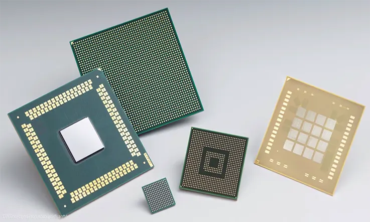
Substrate or PCB (Printed Circuit Board): The substrate serves as the foundation for the µBGA package, providing mechanical support and electrical interconnections. It is typically made of a laminate material with multiple layers of copper traces, vias, and pads.
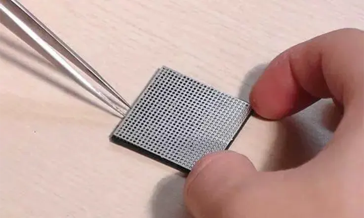
Solder Balls: The solder balls are small spheres of solder alloy (typically lead-based or lead-free) that are attached to the bottom surface of the µBGA package. These solder balls serve as the electrical and mechanical connections between the package and the PCB. They are usually arranged in a grid pattern, forming the ball grid array.
Die/Chip: The die, also known as the chip, is the semiconductor component that contains the integrated circuits (ICs) or other active devices. The die is mounted onto the substrate and wire bonded or flip-chip bonded to establish electrical connections between the die and the substrate.
Underfill Material: The underfill material is a specialized epoxy resin that is injected or dispensed between the die and the substrate. It fills the space between the die and the substrate, encapsulating the wire bonds or solder bumps. The underfill material provides mechanical reinforcement, stress relief, and thermal conductivity, enhancing the reliability of the µBGA package.
It’s important to note that while these are the primary components of a µBGA package, there may be additional elements such as solder mask, solder resist, and protective coatings to provide insulation, protect against environmental factors, and improve reliability. The specific design and composition of these components may vary depending on the requirements of the application and the manufacturing processes used.
µBGA: Design Considerations
When designing with µBGA (micro ball grid array) technology, there are several important considerations to keep in mind. Here are some key design considerations:
1. Package Size and Density:
● Determine the appropriate package size based on the available board space and the desired circuit density.
● Consider the pitch (spacing) between the solder balls to ensure proper routing and manufacturability.
● Balance the need for miniaturization with the requirements for signal integrity, thermal management, and accessibility for testing or rework.
2. Thermal Management:
● Evaluate the thermal requirements of the components and the system to ensure efficient heat dissipation.
● Use appropriate thermal vias and conductive planes in the PCB layout to aid in heat transfer.
● Consider the use of thermal pads or heat sinks on the package to improve thermal performance.
3. Electrical Considerations:
● Pay attention to signal and power integrity to minimize noise and ensure reliable operation.
● Consider impedance control and signal termination techniques to maintain signal quality.
● Optimize power distribution and decoupling capacitor placement to minimize voltage drops and noise.
4. Signal Integrity and Routing Guidelines:
● Follow recommended routing guidelines provided by the manufacturer to maintain signal integrity.
● Minimize signal length and high-speed signal reflections by using controlled impedance traces and avoiding stubs.
● Avoid crossing sensitive high-speed signals with noisy or high-current traces to minimize crosstalk and interference.
5. Manufacturing and Assembly:
● Collaborate with the manufacturing team to ensure that the PCB design meets the assembly requirements for µBGA packages.
● Consider the solder mask and solder paste requirements, pad design, and stencil design for accurate and reliable assembly.
● Verify that the assembly process can accommodate the specific requirements of µBGA, such as ball placement accuracy and reflow temperatures.
6. Testing and Rework:
● Plan for testability during the design phase by including test points and access to critical signals.
● Consider the accessibility of the solder balls for rework or repair, if needed.
● Implement proper test and inspection methodologies to ensure the reliability of the assembled µBGA packages.
It’s essential to consult the datasheets, guidelines, and application notes provided by the specific manufacturer of the µBGA packages you are working with, as they may have additional design considerations and recommendations specific to their products. Additionally, working closely with experienced PCB designers and manufacturing engineers can help ensure a successful design implementation with µBGA technology.
µBGA: Manufacturing and Assembly
Manufacturing and assembly processes for µBGA (micro ball grid array) packages involve several steps to ensure proper placement, attachment, and quality control. Here are some key aspects of the manufacturing and assembly of µBGA packages:

1. PCB Layout Considerations:
● Design guidelines: Follow specific design guidelines provided by the package manufacturer to ensure proper layout and signal integrity.
● Trace routing: Pay attention to trace widths, spacing, and impedance control to maintain electrical performance.
● Thermal considerations: Incorporate thermal vias or thermal pads to aid in heat dissipation from the package.
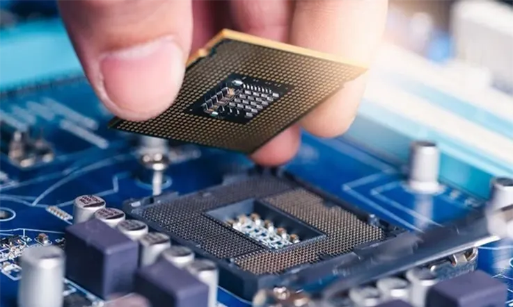
2. Ball Attach and Reflow Process:
● Solder ball attachment: Precise placement of solder balls on the µBGA package using automated equipment, such as pick-and-place machines or specialized dispensing systems.
● Flux application: Apply a flux material to the solder pads on the PCB to promote proper wetting and solder joint formation.
● Reflow soldering: Subject the assembled PCB to a controlled heating process, typically using a reflow oven, to melt the solder balls and establish electrical and mechanical connections.
3. Inspection and Quality Control:
● X-ray inspection: Utilize X-ray equipment to verify proper ball alignment, solder joint quality, and detect any potential defects or voids.
● Automated optical inspection (AOI): Employ AOI systems to perform visual inspections of solder joints, component placement, and overall assembly quality.
● Electrical testing: Conduct electrical tests, such as continuity checks, functional testing, or in-circuit testing, to ensure proper electrical connectivity and functionality of the assembled µBGA packages.
4. Rework and Repair:
● Rework processes: Develop rework procedures to address any defective or improperly connected µBGA packages, including removal of faulty packages, cleaning of solder pads, and re-attachment of new packages.
● Repair techniques: Implement repair techniques, such as soldering or reflowing specific solder joints, to rectify any identified issues during inspection or testing.
It’s important to note that the specific manufacturing and assembly processes may vary depending on the production facility, equipment used, and specific requirements of the µBGA package and PCB design. Manufacturers often follow industry standards, guidelines from package suppliers, and their own internal quality control practices to ensure the reliable assembly of µBGA packages.
µBGA (Micro Ball Grid Array) Defect Inspection
After the soldering process, the detection of defects in Ball Grid Array (BGA) components becomes crucial. Various factors such as component quality, equipment functionality, soldering procedures, and environmental conditions can contribute to the occurrence of defects. These defects encompass issues like open circuits, cold soldering, short circuits, bridging, incomplete soldering, and misalignment. Additionally, problems may arise with the BGA solder balls themselves, such as missing balls and inconsistent sizes.
Inspecting BGAs poses challenges in ensuring the high quality of the final product. This is primarily due to the positioning of the solder balls beneath the visual inspection and the chip, which makes it difficult to identify cavities within the solder joints. Consequently, the inspection process necessitates the utilization of professional and sophisticated equipment to yield accurate results. Advanced methods employed for this purpose include boundary scans, X-ray inspections, and electrical tests.
Traditional electrical testing methods are well-suited for detecting short and open circuits. On the other hand, boundary scan techniques facilitate access to solder joints through boundary connectors, enabling inspection of short and open circuits across interconnected surface-mounted components. Boundary scan methods offer greater efficacy in testing hidden and obscured joints compared to electrical tests. Both methods effectively assess the electrical performance and conductivity of a circuit board. However, they do not assess the quality of solder. Therefore, it is essential to combine these technologies with other methods to evaluate solder quality and identify solder in concealed and invisible joints.
X-ray inspection, performed using X-ray machines, is capable of detecting additional defects that may arise during BGA assembly. This method enables the identification of soldering issues such as solder balls and paste bridging. Some X-ray machines are equipped with software support that can accurately measure the size of solder balls, provided they adhere to established standards. By generating 3D images, a 2D X-ray machine aids in analyzing inner layers, cold soldered joints, blind vias, and vias on soldered joints of BGAs.
Reliability and Failure Analysis of µBGA
Reliability and failure analysis are important aspects of any electronic packaging technology, including µBGA (micro ball grid array). Here are some key points related to reliability and failure analysis in the context of µBGA:
Reliability Testing: Various reliability tests are conducted to ensure the performance and durability of µBGA packages. These tests may include temperature cycling, thermal shock, mechanical shock and vibration, accelerated aging, humidity testing, and solder joint reliability testing.
Failure Modes: Understanding the potential failure modes associated with µBGA packages is crucial for effective analysis and mitigation. Some common failure modes include solder joint failures (such as solder fatigue, solder ball cracking, or solder voids), delamination of the substrate, underfill issues, electrical failures (such as open circuits or shorts), and thermal failures (such as excessive heat generation or thermal mismatch).
Failure Analysis Techniques: When failures occur, failure analysis techniques are employed to identify the root causes. These techniques may include visual inspection, X-ray inspection, acoustic microscopy, dye and pry analysis, cross-sectioning and microscopy, scanning electron microscopy (SEM), energy-dispersive X-ray spectroscopy (EDS), and electrical testing (such as micro-probing and signal integrity analysis).
Design Improvements: Failure analysis provides valuable insights into design weaknesses or manufacturing process issues. The findings can be used to implement design improvements, such as optimizing the layout, adjusting material choices, modifying underfill properties, or enhancing soldering processes.
Reliability Prediction and Modeling: Reliability prediction models, such as the Arrhenius equation or finite element analysis (FEA), can be employed to estimate the long-term reliability of µBGA packages under various operating conditions. These models help in assessing the expected lifespan and identifying potential reliability concerns.
Mitigation Strategies: Based on the failure analysis results, appropriate mitigation strategies can be implemented to enhance the reliability of µBGA packages. These strategies may involve improving the assembly process, optimizing thermal management, modifying materials or underfill formulations, adjusting design parameters, or adopting more robust testing and quality control procedures.
Reliability and failure analysis play a vital role in ensuring the long-term performance and reliability of µBGA packages. By identifying failure mechanisms, addressing design or manufacturing issues, and implementing effective mitigation strategies, manufacturers can enhance the reliability of electronic devices and minimize the risk of failures in the field.
Future Trends and Challenges
Future Trends in µBGA Technology:
Increased Miniaturization: As technology continues to advance, there will be a growing demand for even smaller and more compact electronic devices. This trend will drive the development of µBGA packages with higher density and finer pitch, enabling further miniaturization.
Higher I/O Counts: With the increasing complexity of electronic systems, there will be a need for µBGA packages with higher I/O counts to accommodate the growing number of connections required for data transfer and functionality.
Advanced Materials: The development of new materials with improved thermal conductivity, electrical performance, and reliability will drive the evolution of µBGA packages. These materials may include advanced solder alloys, underfill materials, and substrate materials with enhanced properties.
Integration with Advanced Technologies: µBGA technology will continue to integrate with emerging technologies such as 5G wireless communication, artificial intelligence (AI), Internet of Things (IoT), and augmented/virtual reality (AR/VR). This integration will require innovative designs and packaging solutions to meet the performance demands of these technologies.
Challenges in µBGA Technology:
Thermal Management: As electronic devices become more compact and powerful, managing heat dissipation becomes increasingly challenging. The small size of µBGA packages can limit the effectiveness of traditional cooling solutions, requiring the development of advanced thermal management techniques to prevent overheating and ensure reliable operation.
Signal Integrity: The high-density nature of µBGA packages can lead to signal integrity issues such as crosstalk, noise, and signal degradation. Designers will need to implement effective signal integrity measures, including controlled impedance routing, power distribution, and noise suppression techniques, to maintain signal quality.
Manufacturing Complexity: The small size and high-density of µBGA packages present manufacturing challenges, including precise ball placement, accurate soldering, and inspection difficulties. Manufacturers will need to invest in advanced assembly and inspection equipment to ensure reliable and cost-effective production.
Reliability: Ensuring the long-term reliability of µBGA packages is crucial, especially in applications where vibrations, shocks, and thermal cycling are common. Factors such as material selection, underfill processes, and testing methodologies will need to be optimized to enhance the reliability and robustness of µBGA packages.
Addressing these challenges will require collaboration between semiconductor manufacturers, packaging companies, and design engineers to develop innovative solutions and manufacturing techniques that meet the evolving needs of the industry.
In a Words
µBGA (micro ball grid array) technology offers several advantages and finds a wide range of applications in various industries. The compact size and high circuit density of µBGA packages enable miniaturization and facilitate the design of smaller and more functional electronic devices. The increased I/O density allows for a higher number of connections within a limited space.
Furthermore, µBGA packages exhibit improved electrical performance due to shorter electrical path lengths and reduced parasitic capacitance and inductance. This enhances signal integrity and overall electrical performance. The small package size also contributes to efficient heat dissipation, leading to improved thermal management.
From a manufacturing perspective, µBGA technology offers cost-effective solutions. The automated assembly processes result in higher production yields and lower manufacturing costs compared to larger package options.
The applications of µBGA technology are vast and diverse. It is extensively used in consumer electronics such as smartphones, tablets, and digital cameras, where compact size and high functionality are essential. Additionally, IoT devices, automotive electronics, medical devices, and aerospace and defense systems benefit from µBGA technology due to its space-saving capabilities and reliability.
Overall, µBGA technology continues to advance, enabling the development of smaller, more powerful, and highly functional electronic devices across various industries. As technology evolves, we can expect further advancements in µBGA design, manufacturing processes, and applications, fueling innovation in the electronics industry.