
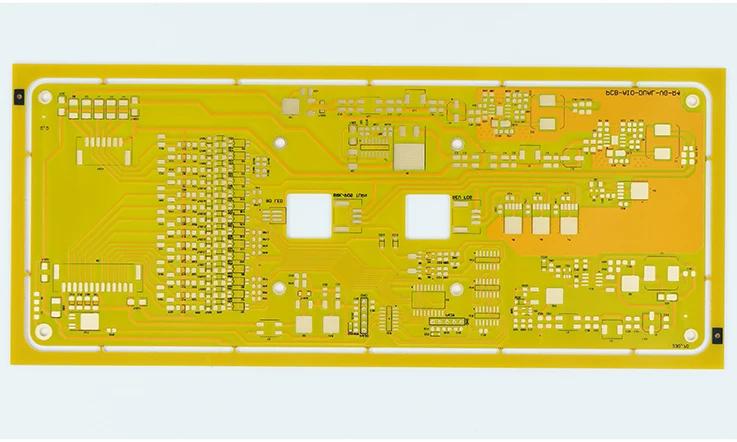
NELCO N4000-2 laminate represents a tailored solution for multilayer circuit boards requiring stable electrical performance with low dielectric loss and a controlled dielectric constant. Its capacity to maintain signal integrity at high frequencies, including GHz and mmWave ranges, makes it suitable for sophisticated digital, RF, and microwave designs deployed in military, telecommunications, and medical sectors. The material’s dimensional stability, thermal management, and compatibility with mixed-dielectric stack-ups offer flexibility in multilayer system architectures.
Additionally, manufacturing considerations such as resin flow control and prepreg balance contribute to reducing common fabrication challenges like delamination and micro-cracking. This comprehensive overview covers comparative analyses, layer stack strategies, and practical fabrication insights aligned with advanced PCB design and production techniques.
Introduction to NELCO N4000-2 PCB Materials and Applications
The selection of base materials for multilayer circuit boards directly influences signal performance, thermal behavior, and fabrication reliability. Among mid-loss laminate systems, NELCO N4000-2 PCB delivers stable electrical behavior and supports various processing requirements across different application scenarios. This material is often applied in advanced circuit board layouts used in aerospace control modules, medical imaging systems, and telecommunications equipment.
This section presents an overview of the material’s composition, its main industrial applications, and recent global usage trends across sectors involved in high-frequency and high-density interconnect systems.
What Is NELCO N4000-2 PCB Laminate?
NELCO N4000-2 is a glass-reinforced, multifunctional epoxy laminate designed for multilayer PCB applications. Its mechanical and electrical properties remain stable across various operating conditions, making it suitable for both digital and RF circuit configurations. Built on a high glass transition temperature (Tg) epoxy resin system, this laminate maintains performance under elevated thermal loads and repeated reflow cycles.
The material’s dielectric constant (Dk) remains within a predictable range of 4.1 to 4.3, making it compatible with impedance-controlled designs. Dissipation factor (Df) is maintained between 0.017 and 0.023, which minimizes signal attenuation over distance and frequency. This behavior supports reliable operation in designs up to several GHz.
A technical overview is shown below:
| Property | Typical Values | Test Method Reference |
| Dielectric Constant (Dk) | 4.3 @ 1 MHz | IPC-TM-650 2.5.5.3 |
| Dissipation Factor (Df) | 0.023 | IPC-TM-650 2.5.5.3 |
| Glass Transition Temperature | 130 – 140°C | IPC-TM-650 2.4.25c |
| Thermal Conductivity | Approx. 0.3-0.4 W/m·K | ASTM E1461 |
| Volume Resistivity | 107 – 108ohm·cm | IPC-TM-650 2.5.17.1 |
| Surface Resistivity | 107 ohm | IPC-TM-650 2.5.17.1 |
| UL Flammability Classification | 94V-0 | UL 94 |
This combination of attributes supports the material’s integration in multi-functional boards while maintaining processing flexibility with traditional FR-4 production lines.
Primary Use Cases in Military, Medical, and 5G Infrastructure
The NELCO N4000-2 PCB laminate supports a wide range of systems that require predictable electrical and thermal behavior. Specific use cases include:
Defense Applications-
Multilayer boards in radar systems, avionics control units, and satellite communications often rely on material systems with stable thermal expansion and low dielectric variability. N4000-2 enables the creation of consistent impedance traces and multi-signal layer stacks required in compact and high-density defense electronics.
Medical Equipment-
In areas such as diagnostic electronics, modular ultrasound probes, and digital imaging, signal integrity and layer reliability are primary concerns. The epoxy-glass formulation of NELCO N4000-2 facilitates fine-line design, stable Dk, and compatibility with solder reflow cycles, supporting multi-cycle sterilization and long product life spans.
5G Networking Systems-
As 5G expands globally, base stations, remote radio heads, and millimeter-wave modules are increasingly built on low-loss laminate materials. The Df and thermal behavior of N4000-2 allow it to support these higher frequency signals while maintaining process yields similar to standard FR-4 processes.
Global Demand Trends and Industrial Adoption
In recent years, the demand for NELCO N4000-2 PCB laminates has grown across several industrial regions. This material has been adopted in telecommunications baseband platforms, automotive radar modules, and edge computing hardware by those involved in circuit layout and fabrication processes.
Several factors contribute to its increasing use:
●Compatibility with existing fabrication equipment and chemical processes;
●Stability of dielectric performance in stacked microvia and HDI configurations;
●Repeatable mechanical behavior across reflow and thermal shock cycles.
Regions including North America, Germany, Southeast Asia, and South Korea are seeing higher integration rates of NELCO N4000-2 PCB materials, particularly in industries focused on embedded computing, wireless transmission, and precision instrumentation.
Why NELCO N4000-2 PCB for High-Speed Digital, RF, and Microwave Applications?
NELCO N4000-2 PCB laminates are frequently selected for multilayer circuit designs handling high-frequency, high-density signals across digital, RF, and microwave systems. Their role in signal transmission reliability, impedance control, and layer stack integrity helps address requirements in advanced PCB structures used in telecommunications, radar, and high-throughput processing. This section outlines how N4000-2-based PCBs perform across three technical domains—GHz digital design, microwave circuit layout, and mmWave/radar signal paths—focusing on measurable behaviors and layout results at the circuit level.
Performance in GHz Range Digital Circuits
In digital PCB design, particularly above 1 GHz, trace routing, return path continuity, and via transition effects begin to dominate signal behavior. The NELCO N4000-2 laminate supports stable performance across multilayer interconnects, helping reduce delay skew and signal reflection issues.
Trace Impedance Consistency Across Layers-
NELCO N4000-2 PCBs support uniform dielectric behavior throughout stackups, helping maintain 50-ohm and 100-ohm differential impedance in microstrip and stripline routing for DDR4, SerDes, and USB 3.0+ designs.
Signal Integrity in Dense Interconnects-
Designs with tight BGA breakout regions benefit from minimal crosstalk due to the laminate’s predictable dielectric spacing and controlled glass weave, supporting equal length routing and matched impedance across differential pairs.
Vias and Transition Regions-
NELCO N4000-2 boards support stable signal behavior during layer transitions through vias. When backdrilling and anti-pad dimensions are tuned appropriately, reduced insertion loss has been observed, even when routing PCIe Gen4/5 across more than four layers.
Design Considerations for Microwave Frequencies
For circuits operating in microwave bands (1 GHz to 30 GHz), board-level behavior depends on the layout of transmission lines, transitions into connectors, and the shielding effectiveness between RF zones and digital blocks.
Transmission Line Uniformity-
Coupled or uncoupled stripline structures implemented on N4000-2 boards have demonstrated repeatable S-parameter characteristics. Controlled dielectric layering supports smoother transitions between edge launch connectors and internal routing paths.
RF Cavity Isolation-
In hybrid boards combining analog and RF zones, NELCO N4000-2 maintains stable mechanical properties across cavities, which helps retain defined separation between RF, control, and DC bias paths. Shielding vias and ground stitching continue to perform effectively even with complex multilayer routing.
Impedance-Matched Routing Across Layers-
For layouts including Wilkinson splitters, directional couplers, or amplifier bias tees, the dielectric structure supports gradual impedance tapers and stub lengths, which directly affect S11/S21 behavior.
Compatibility with mmWave and Radar Systems
In mmWave and radar system boards, signal routing above 30 GHz places constraints on trace surface finish, dielectric homogeneity, and layer-to-layer alignment. The N4000-2 PCB stackups enable reproducible layout across phased-array, beamforming, or automotive radar platforms.
Controlled Delay Matching Across Phase Lines-
Multichannel systems using phase-matched interconnects have shown improved alignment across beamforming elements, where N4000-2 supports low-loss dielectric pathways that help minimize phase drift under varying environmental conditions.
Low Skew Differential Transmission-
In radar front-end designs, low skew across symmetrical pairs routed in parallel planes (for example, in FMCW radar processing) ensures better range resolution. PCB designs using NELCO N4000-2 show fewer delay mismatches across layers in back-to-back measurements.
Environmental Stability in Harsh Deployments-
From aerospace to industrial radar systems, boards fabricated with NELCO N4000-2 show limited variation in dielectric behavior under humidity cycling, thermal exposure, or mechanical vibration, which helps maintain time-of-flight accuracy and stable SNR in radar receivers.
Technical Specifications and Electrical Performance of NELCO N4000-2
Understanding how a laminate performs across electrical, mechanical, and thermal domains is a necessary step when selecting a suitable base material for multilayer printed circuit boards. NELCO N4000-2 PCB laminate supports predictable results in controlled impedance, high-frequency routing, and thermal endurance. This section outlines the main electrical characteristics and compliance behaviors that support its use in advanced circuit designs across varied industries.
Dielectric Properties (Dk/Df) for Signal Integrity
Signal fidelity in high-speed environments depends on reliable dielectric behavior. NELCO N4000-2 PCB materials are engineered with a stable dielectric structure that supports differential signaling and maintains controlled impedance during transitions between layers.
●Dielectric constant (Dk): Maintains values between 4.1–4.3, measured up to 10 GHz, supporting stable transmission line behavior.
●Dissipation factor (Df): Ranges from 0.017 to 0.023, allowing reduced insertion loss across extended signal paths.
●Application in multilayer designs: Enhances accuracy in impedance modeling and reflection control for high-speed interfaces like PCIe and DDR.
This performance makes NELCO N4000-2 PCB laminates well-suited for scenarios requiring rigorous control over trace geometry and signal velocity.
CAF Resistance and High Tg for Harsh Conditions
We often face challenges when circuits are expected to perform across fluctuating humidity and elevated temperatures. The NELCO N4000-2 PCB laminate addresses these scenarios with its insulation strength and thermal durability.
●CAF resistance: Validated in 85°C/85%RH environments under bias, reducing risk of conductive failure between vias and inner layers.
●Glass transition temperature (Tg): Consistently in the 135–140°C range, permitting use in lead-free reflow cycles.
●Layer bond reliability: Withstands thermal shock and cycle exposure from −40°C to +125°C, aiding deployment in rugged electronic platforms.
| Property | Value / Range | Notes |
| CAF Resistance | 85°C/85%RH under bias | Reduces risk of conductive failures |
| Glass Transition Temp (Tg) | 135–140°C | Supports lead-free reflow |
| Thermal Cycle Range | −40°C to +125°C | Suitable for rugged platforms |
Such features make this material suitable for use in defense radar systems, satellite electronics, and high-voltage control modules.
Compatibility with Lead-Free and Halogen-Free Standards
Meeting global environmental and safety standards is a common design requirement. NELCO N4000-2 PCB laminates are aligned with multiple fabrication specifications to reduce compliance risks in regulated markets.
●Lead-free process compatibility: Tolerates reflow peaks exceeding 260°C without delamination, supporting SAC solder alloy profiles.
●Halogen-free option: Offers resin systems that meet IEC 61249-2-21 standards for low halogen emissions.
●UL 94V-0 rating: Achieves required flammability classification, expanding application in medical, telecom, and aerospace circuit boards.
| Property | Value / Range | Notes |
| Lead-Free Reflow Tolerance | >260°C | Compatible with SAC solder |
| Halogen-Free Compliance | IEC 61249-2-21 | Meets low halogen standards |
| UL Flammability Rating | UL 94V-0 | Approved for sensitive sectors |
These characteristics simplify integration into international workflows where green materials and long-term reliability are requested.
Comparing NELCO N4000-2 with FR4, Rogers, and Isola Materials
Choosing the right PCB laminate system for multilayer PCB design in aerospace, telecommunications, and medical electronics requires close scrutiny of electrical performance, thermal behavior, mechanical durability, and fabrication compatibility. NELCO N4000-2 distinguishes itself from traditional FR4, premium Rogers series, and select Isola materials by providing a balance of low Dk, controlled Df, and stable z-axis expansion that fits high-frequency and high-speed applications.
This section explores performance benchmarks across material types, guiding our engineering teams and PCB designers to make data-informed selections aligned with technical and commercial objectives.
Electrical and Mechanical Differences
Evaluating performance requires comparison across standardized parameters such as dielectric constant (Dk), dissipation factor (Df), glass transition temperature (Tg), and z-axis coefficient of thermal expansion (CTE).
Dielectric Properties-
NELCO N4000-2 maintains a stable Dk of approximately 4.1 at 1 GHz and a Df of 0.009, making it suitable for designs requiring consistent impedance and reduced insertion loss. Standard FR4 exhibits Df values often exceeding 0.018–0.022, limiting its use in high-speed signal environments. Rogers RO4003C offers lower Df (~0.0027), suitable for RF systems, but requires stricter processing conditions.
Thermal Expansion and Dimensional Control-
NELCO N4000-2 exhibits a z-axis CTE between 230–260 ppm/°C, with good via protection during lead-free reflow cycles. This contrasts with traditional FR4 materials, which often exceed 300 ppm/°C post-Tg, increasing the likelihood of interconnect stress or delamination. Isola 370HR and Rogers 4350B offer improved z-axis behavior, yet at higher cost and complexity.
Mechanical Response to Thermal Cycling-
The glass transition temperature of N4000-2 is rated at 175 °C. This allows repeated exposure to reflow temperatures above 260 °C without excessive resin degradation or delamination. For applications involving frequent thermal cycling, such as automotive radar units or edge computing modules, this parameter is particularly useful.
Comparative Table – Performance Benchmarks-
| Property | NELCO N4000-2 | Standard FR4 | Rogers RO4003C | Isola 370HR |
| Dk @ 1 GHz | 4.1 | 4.2–4.6 | 3.38 | 3.9 |
| Df @ 1 GHz | 0.009 | 0.018–0.022 | 0.0027 | 0.012 |
| Tg (°C) | 175 | 130–150 | >280 | 180 |
| CTE z-axis (ppm/°C, post-Tg) | 230–260 | 300–350 | <200 | ~250 |
| Lead-Free Reflow Compatibility | Stable | Limited | Very Stable | Stable |
This data provides a clear structure for comparing mechanical and electrical behaviors among common laminate systems.
Application-Specific Recommendations
Material selection must align with the performance targets and compliance requirements of specific application areas. The following use cases illustrate how NELCO N4000-2 applies across distinct sectors:
Telecommunications Systems-
NELCO N4000-2 supports impedance-controlled signal layers in backplane, switch, and RF front-end circuits without requiring PTFE-based materials. Its dielectric profile suits designs above 1 GHz where FR4 would incur signal degradation.
Medical Device Electronics-
Diagnostic equipment such as portable ECG monitors, ultrasound platforms, and sensor arrays benefit from N4000-2’s stable dielectric behavior and thermal durability. The material supports predictable signal paths while minimizing variations related to the base material during production.
Aerospace and Military Systems-
For avionics interface boards, missile communication links, and radar subassemblies, N4000-2 offers fabrication reliability under moderate frequency demands. In contrast, high-end Rogers or Isola materials are reserved for very high-frequency applications exceeding 10 GHz.
Application-to-Material Fit Matrix-
| Application Category | FR4 | NELCO N4000-2 | Rogers RO Series | Isola High-Speed |
| Low-Speed Digital Control | ✓✓ | ✓✓ | – | – |
| 1–5 GHz Signal Routing | – | ✓✓✓ | ✓✓✓✓ | ✓✓✓ |
| Imaging & Diagnostics | – | ✓✓✓ | ✓✓✓✓ | ✓✓✓ |
| Satellite & Radar Systems | – | ✓✓ | ✓✓✓✓✓ | ✓✓✓✓ |
These examples reflect the practical deployment of each material class across real-world engineering environments.
Total Cost of Ownership and ROI Analysis
When evaluating materials beyond initial purchase price, it is need to consider their impact on process yield, rework frequency, and field reliability.
Procurement and Fabrication Economics-
NELCO N4000-2 provides lower total procurement cost than Rogers 4350B and Isola Tachyon 100G, especially in batch quantities. It also supports conventional lamination equipment and standard drilling processes, minimizing fabrication setup cost.
Yield Rates and Board Reliability-
With lower out-of-plane expansion and consistent Tg behavior, N4000-2 increases multilayer board yield in HDI, sequential lamination, and controlled-impedance applications. The reduced incidence of delamination improves process repeatability.
Lifecycle Durability and Operational Return-
Field-deployed devices benefit from the resin stability and mechanical uniformity of N4000-2, reducing the risk of early failure due to thermal fatigue. Over a 3–5 year product lifecycle, this contributes to measurable reductions in return rates.
ROI Analysis by Material Type-
| Metric | FR4 | NELCO N4000-2 | Rogers 4350B | Isola Tachyon |
| Material Cost per Panel | Low | Moderate | High | High |
| Compatibility with Standard Process | High | High | Medium | Medium |
| HDI/Sequential Lamination Yield | Medium | High | High | High |
| Lifecycle Stability | Medium | High | Very High | Very High |
| 3-Year Return on Investment | Moderate | High | Conditional | Conditional |
This data-driven framework supports better planning across product engineering, purchasing, and production departments.
Layer Stack-Up Strategies Using NELCO N4000-2 Laminates
The construction of multilayer printed circuit boards using NELCO N4000-2 laminates involves meticulous planning of layer stacking to optimize electrical performance and mechanical stability. Combining NELCO epoxy-based laminates with materials like PTFE allows adjustment of dielectric properties, enabling control over signal propagation and thermal expansion within complex layer arrangements. The following sections discuss approaches to mixed-dielectric stack-ups, maintaining signal integrity across layers, and manufacturing considerations relevant to multilayer system fabrication.
Mixed-Dielectric Stack-Up with NELCO and PTFE
The integration of NELCO N4000-2 with PTFE laminates forms a hybrid dielectric structure tailored to balance electrical and mechanical characteristics in high-frequency applications.
●Dielectric constants of NELCO N4000-2 (~3.48 at 10 GHz) and PTFE (~2.1) are arranged to achieve desired impedance and signal velocity through selective layer placement.
●Coefficients of thermal expansion differ between epoxy and PTFE, requiring careful stack sequencing and material matching to reduce mechanical strain during thermal cycling.
●Loss tangent management is addressed by placing low-loss PTFE near high-speed signal layers while using NELCO laminates for structural rigidity and manufacturability.
Signal Integrity Control Across Layers
Effective signal transmission within multilayer boards built with NELCO N4000-2 depends on maintaining uniform impedance, precise layer alignment, and stable dielectric properties.
●Accurate dielectric property characterization supports impedance tuning to minimize signal reflections and insertion loss.
●Precise layer registration reduces misalignment, limiting signal path discontinuities and crosstalk.
●Matching trace lengths and dielectric properties across layers helps balance signal timing and reduce skew in differential pairs.
Manufacturing Considerations for Multilayer Systems
Producing multilayer PCBs with NELCO N4000-2 involves managing resin flow, prepreg behavior, and curing parameters to ensure lamination quality and electrical reliability.
●Resin content and flow during lamination presses are monitored to prevent voids and delamination in the epoxy resin matrix.
●Cure profiles are developed to align with the glass transition temperature and reaction kinetics of the N4000-2 material, ensuring thorough polymerization.
●Design of symmetrical stack-ups and control of layer count assist in reducing panel warpage and mechanical distortion during fabrication.
Advanced NELCO N4000-2 PCB Design Considerations
As multilayer PCB applications become increasingly data-intensive and frequency-driven, selecting appropriate design methodologies becomes a necessity rather than an option. The NELCO N4000-2 laminate is engineered for high-frequency circuits, and achieving optimum performance from it requires deep technical insight. This section explores design-stage choices involving stack-up configurations, signal behavior at high-speed operation, and thermal stress control — with all insights aligning closely with practical field demands across aerospace, RF communication, defense-grade systems, and medical imaging platforms.
Layer Stack-Up Best Practices
Proper stack-up configuration influences impedance control, mechanical integrity, and manufacturing yield. NELCO N4000-2 PCB laminates offer balanced dielectric profiles across multiple layers, enabling predictable electrical responses in RF and high-speed designs.
●Symmetrical Layer Distribution: Maintain symmetry in prepreg and core layers using the NELCO N4000-2’s available variants (e.g., N4000-2 SI, N4000-2 HF) to reduce warpage and bow.
●Power-Ground Plane Proximity: Utilize close coupling between power and ground planes to minimize loop inductance. NELCO N4000-2 materials support tight dielectric spacing down to 3 mils for dense inner-layer structures.
●Consistent Copper Weight Usage: Apply uniform copper thickness (e.g., 0.5 oz or 1 oz) across signal layers to help prevent uncontrolled impedance variance. This is particularly beneficial in applications requiring 50-ohm or 100-ohm differential pairs.
Common Stack-Up Configurations for NELCO N4000-2-
●6-layer HDI: Core-prepreg-core with dual power planes
●8-layer RF interface: Top-layer ground shielding with embedded microstrip routing
●12-layer signal-dense: Interleaved power distribution using multiple N4000-2 HF cores
Signal Integrity Optimization for High-Speed Circuits
NELCO N4000-2 laminates exhibit stable dielectric constant (Dk) and low dissipation factor (Df), ensuring transmission quality under gigabit data rates. Engineers focusing on SI performance can take advantage of these predictable parameters across the entire operating bandwidth.
●Controlled Dk for Consistent Timing: With Dk ~4.1 @ 1 GHz, NELCO N4000-2 reduces signal skew, making it suitable for edge-sensitive applications like DDR4 routing or 10GBASE-KR backplanes.
●Low Df for Minimal Signal Loss: The 0.023 (@ 1 MHz) dissipation factor keeps insertion loss under check, especially over long traces or backplane segments. Differential routing on inner layers benefits from N4000-2’s reduced dielectric absorption.
●Impedance Matching Techniques: Combine field solvers with known material properties of NELCO N4000-2 to model trace dimensions. Avoid mismatched trace pairs which can induce reflections in LVDS and SerDes layouts.
Practical Signal Integrity Use Cases-
●10 Gbps Ethernet interconnects across 18″ multilayer PCBs
●USB 3.2 Gen 2 differential pairs routed with <±10% impedance deviation
●High-resolution ADCs operating above 1 GS/s in imaging devices
Thermal Management and CTE Stability in Design Phase
Beyond electrical requirements, the NELCO N4000-2 laminate addresses mechanical demands under varied operating temperatures. Therefore, we need to align thermal expansion characteristics with chosen components and plating systems.
●CTE Matching to Copper and Vias: The z-axis CTE of <50 ppm/°C reduces stress on plated through holes during solder reflow, improving structural stability in BGA-heavy layouts.
●Tg > 175°C for Solder Cycling Durability: High glass transition temperature (Tg) reduces deformation risk during assembly processes involving multiple IR reflows.
●Layered Heat Distribution Strategy: Combine thermal vias and plane layers around heat sources to dissipate energy efficiently. NELCO N4000-2’s resin system supports high-power applications such as RF amplifiers and FPGA thermal cores.
Laminate Stability During Thermal Cycling-
●Reflow profile tolerance: 260°C peak for Pb-free solder
●IPC-4101 /21, /24 compliance for elevated thermal endurance
●Less than 0.7% Z-axis expansion up to Tg
NELCO N4000-2 PCB Manufacturing Guidelines and Tips
Obtaining reliable outcomes with NELCO N4000-2 in multilayer PCB fabrication requires thorough knowledge of how its thermomechanical and dielectric properties interact with manufacturing procedures. Its elevated Tg, minimal Z-axis expansion, and resin attributes align well with advanced lamination cycles, high-aspect-ratio drilling, and durable via formation. Still, maximizing performance calls for precise process management throughout lamination to post-etch cleaning stages.
Lamination Parameters and Drilling Considerations
NELCO N4000-2 demonstrates stable flow behavior and dimensional control during high-pressure lamination, even in complex stack-ups with multiple signal and power planes. It responds well to prepreg bonding and provides reliable bonding strength across layers—assuming process heat-up rate and pressure are optimized.
Thermal Cycle Recommendations for Lamination Precision-
Suggested press cycles include a pre-heating ramp of 2.5–4°C/sec to approximately 180°C, followed by a full cure near 200–210°C for at least 60 minutes under vacuum. Lamination pressure of 300–400 psi, depending on the layer count and copper thickness, supports uniform resin flow.
Drill Entry and Exit Material Choices Reduce Smearing-
To mitigate drill smear and maintain hole quality, use laser-drilled entry and exit materials with optimized bit geometry (135° split point preferred). Bit replacement intervals should match the resin-glass interface hardness to avoid delamination.
Managing Glass-Reinforced Layer Stack-Ups-
For high-layer-count boards, staggered glass styles such as 2116 or 7628 can be selected to improve registration and reduce drill breakout. Tight pitch vias (<0.25 mm spacing) benefit from resin systems with controlled flow profiles.
Surface Preparation for Optimal Adhesion
Surface quality directly influences copper-to-laminate adhesion, especially when working with ENIG, immersion silver, or OSP finishes. The NELCO N4000-2 PCB surface resists oxidation and etching inconsistencies under controlled preparation protocols.
Desmear Process Tailored to Resin Characteristics-
Plasma or permanganate desmear should be applied with precise timing to avoid over-etching. Excessive exposure may erode glass bundles or alter the inner layer trace geometry, particularly in fine-line circuits below 100 µm.
Debris-Free Hole Walls via Micro-Etching-
Post-drill cleaning with acid micro-etch or plasma treatments enhances hole wall cleanliness prior to plating. Maintaining uniform inner diameter roughness supports stronger copper adhesion and stable electrical continuity.
Adhesion Testing Before Soldermask Application-
Conduct pull-strength or peel-back tests after oxide or black oxide treatments to confirm copper-laminate bond integrity. Optimal performance is seen when contact angle is reduced below 30° after chemical cleaning.
Via Reliability and Resin Flow Control
Microvias, through-holes, and stacked vias are widely used in high-density interconnects. The resin behavior of NELCO N4000-2 contributes to excellent via fill performance and dielectric reliability—but only when resin flow, press parameters, and via geometry are tightly controlled.
Resin Flow Monitoring in High-Aspect-Ratio Structures-
Flow front simulation during lamination can help avoid resin starvation in narrow channels. For via fills, keep aspect ratios below 10:1 and consider staggered microvias instead of stacked vias when layer spacing is below 75 µm.
Copper Balance and Inner Layer Flatness Improve Via Quality-
Maintain symmetrical copper distribution to avoid z-axis warpage during lamination. Uneven pressure or thermal mismatch across asymmetrical layers can cause via distortion or annular ring shift.
Post-Etch Cleaning for Via Metallization Uniformity-
Prior to electroless copper plating, apply horizontal scrubbing and soak cycles to remove oxide residues. This reduces surface tension anomalies and supports uniform metallization down the hole barrel.
Common Issues and Solutions in NELCO N4000-2 PCB Fabrication
Fabrication multilayer PCBs with NELCO N4000-2 calls for precise management of the process environment, particularly when targeting high-density interconnects, narrow trace widths, and durability through reflow or thermal shock cycles. In real-world production, issues like delamination, resin starvation, and micro-cracking can develop when the relationship between material behavior and manufacturing conditions is not carefully addressed.
Preventing Delamination during Reflow
Delamination typically arises from excessive moisture absorption, improper lamination temperature, or insufficient oxide treatment. NELCO N4000-2’s high Tg value and moisture resistance enhance thermal robustness, but the process window must remain tightly managed.
| Parameter / Action | Recommended Value / Method | Purpose |
| Vacuum Lamination | >27 inHg | Enhances consolidation and resin flow |
| Pre-Dry Temperature & Duration | 125°C for 4 hours | Reduces moisture absorption |
| Surface Preparation | Plasma desmear + microetch | Promotes interlayer adhesion |
| Reflow Validation Method | IPC-TM-650 2.6.27 | Simulates thermal stress for IPC Class 3 |
| Reflow Simulation Test | Six-zone oven profile | Models cumulative thermal exposure |
●Maintain vacuum lamination above 27 inHg with pre-dried prepreg and cores at 125°C for 4 hours.
●Apply plasma desmear and microetch to promote bonding strength in high-layer-count builds.
●Use IPC-TM-650 Method 2.6.27 to validate reflow resistance in design-specific thermal profiles.
When reflow profiling does not match the thermal characteristics of the resin system, even high-Tg laminates such as NELCO N4000-2 may exhibit interlayer separation.. PCB Manufacturers producing IPC Class 3 boards should incorporate a six-zone reflow oven test to simulate cumulative thermal load across production.
Managing Resin Flow and Prepreg Balance
Balanced resin flow ensures proper via fill, minimizes voiding, and prevents glass cloth exposure on outer layers. For NELCO N4000-2, resin distribution is a matter of prepreg layer count, press pressure ramp rate, and oxide surface conditioning.
| Parameter / Stack-Up Consideration | Recommended Practice | Functionality |
| Prepreg Pairing | Symmetric layup (e.g., 1080/2116 or 2116/7628) | Stabilizes resin flow across core |
| Pressure Ramp Rate | 50 psi/min | Controls gelation phase |
| Final Lamination Pressure | 350–400 psi | Ensures via encapsulation and uniformity |
| Compatibility Test | Hybrid flow window check | Validates flow with PTFE/LCP combinations |
| Resin Flow Evaluation | Coupon-based monitoring at drilled vias | Confirms material distribution under stress |
●Stack symmetric prepreg constructions (e.g., 1080/2116 or 2116/7628) around core laminates to stabilize flow
●Set lamination pressure ramp-up to 50 psi/min, targeting hold pressure of 350–400 psi during gelation
●Verify flow window compatibility with hybrid stack-ups involving PTFE or LCP dielectric materials
The flow characteristic of N4000-2 resin systems has been optimized to accommodate tight-pitch BGA designs and sequential lamination cycles. A test coupon program evaluating resin movement around mechanically drilled vias is recommended for each new stack-up.
Avoiding Voids and Micro-Cracking
Voids and micro-cracks are typically linked to insufficient degassing, poor oxide treatment, or excessive mechanical stress during panel handling. Such defects may severely affect reliability in high-speed signal environments and thermal cycling conditions.
| Action / Control Point | Recommended Value / Tool | Purpose |
| Pre-Bake Procedure | 120°C for 2–4 hours | Eliminates residual moisture before lamination |
| Surface Conditioning | Brushing or pumice scrubbing | Improves oxide adhesion uniformity |
| Micro-Crack Inspection | Cross-sectioning per IPC-6012 | Identifies voids and crack propagation zones |
| Drilling Adjustment | Reduce dwell time by 15% | Minimizes z-axis stress and delamination risk |
| Drill Tool Selection | Undercut bits with CFR (chip flush removal) tools | Enhances reliability in high-aspect vias |
●Pre-bake inner layer materials at 120°C for 2–4 hours to remove absorbed moisture
●Apply controlled mechanical brushing or pumice scrubbing to ensure oxide uniformity and adhesion
●Use cross-sectional micro-sectioning per IPC-6012 to inspect resin coverage and crack propagation zones
In aerospace-grade PCB applications, micro-cracking has been traced back to aggressive drilling parameters and unbalanced z-axis expansion. For NELCO N4000-2, a drill dwell time reduction by 15% and use of undercut bits with CFR tools have shown positive yield improvements.
Why Select JarnisTech for NELCO N4000-2 PCB Fabrication?
The selection of a fabrication partner for NELCO N4000-2 PCBs demands precision, process transparency, and extensive material knowledge. In high-frequency and high-layer-count board production, the interaction between laminate properties and process control determines outcomes across telecommunications, aerospace, and advanced medical systems. JarnisTech applies a controlled methodology, using internal verification protocols, storage management systems, and traceable processing standards designed specifically for high-performance thermoset epoxy laminates.
Below, we examine decisive considerations for working with JarnisTech on N4000-2 PCB manufacturing.
Selection Standards for NELCO-Based PCB Production
PCB procurement for microwave, radar, and high-speed interconnect projects is best guided by specific evaluation benchmarks. JarnisTech addresses each with structured quality controls and material assurance.
●Material Matching by Specification Sheet: NELCO N4000-2 laminates differ in glass transition temperature, dielectric properties, and thermal endurance. JarnisTech inspects each incoming lot and verifies alignment with IPC-4101/29 and /126 classifications before defining the stack-up.
●Capability for Complex Stack-Up Execution: From hybrid dielectric combinations to high-aspect-ratio via formation, the facility’s capability extends to impedance-controlled structures and cavity boards, with lamination techniques tuned to NELCO curing dynamics.
●Conformance to ISO and MIL Standards: Traceable document control, RoHS lead-free protocols, and Class 3 (IPC-A-600) acceptance criteria are enforced. Reports and batch data can be delivered in real time for high-reliability projects.
The selection process should never hinge on price alone. Material traceability, panel handling precision, and repeatability from one lot to another make a measurable difference when working with high-speed laminates.
Controlled Storage for Laminate Stability
Epoxy-based laminates such as N4000-2 require careful handling once received at the fabrication site. Moisture absorption, storage temperature variation, and prepreg shelf-life impact bond strength and interlayer alignment. JarnisTech’s systems counter these risks with documented control points.
●Humidity-Controlled Warehousing: All prepregs and cores are sealed with desiccant packs and tracked under FIFO policy. Daily checks verify temperature and relative humidity conditions remain within vendor-recommended limits.
●Lot Tracking by QR-Coded Inventory: Each roll or panel of N4000-2 laminate is tagged for batch traceability. Automated logs record handling events and aging curves, avoiding expired material use during layup.
●Pre-Bake Procedures before Lamination: To remove residual moisture and stabilize the dielectric before press, pre-bake cycles are applied per NELCO’s application notes. Controlled vacuum ovens ensure temperature uniformity across panels.
Correct storage influences press performance, interface integrity, and final electrical characteristics. Ignoring these controls may not cause immediate issues, but downstream failures in signal loss or delamination often trace back to early material mishandling.
Internal Validation and Testing Capabilities
Once fabrication begins, stable electrical behavior and structural integrity rely on embedded testing and quality monitoring throughout the process. JarnisTech applies a full range of laboratory and in-line inspection methods specifically configured for boards built with NELCO materials.
●Capacitance and Impedance Test Coupons: Integrated into production panels, these allow real-time measurement of impedance behavior, resin distribution, and interconnect alignment during the build process.
●Solder Float and T260/T288 Testing: Boards are validated using IPC-TM-650 tests to verify thermal integrity. Resin decomposition resistance and delamination thresholds are benchmarked against datasheet values.
●AOI and X-ray Inspection across Layers: Multilayer alignment, via registration, and void analysis are executed through non-destructive scanning. X-ray results are used for in-process tuning of drill and plating parameters.
Rather than rely on third-party inspections post-production, JarnisTech conducts evaluations in-house and immediately addresses deviations. This shortens the feedback loop and increases confidence in repeat production runs.
NELCO N4000-2 PCB – FAQ
1.What types of copper foil can be used with NELCO N4000-2 laminates?
Reverse-treated, HTE, and low-profile copper foils are commonly supported, including VLP and HVLP variants.
2.Can NELCO N4000-2 be used in backplane or high-layer-count PCBs?
Yes, it is widely used in 16+ layer designs, including high-speed backplanes and dense signal routing environments.
3.Does NELCO N4000-2 support blind and buried vias?
Yes, this laminate is suitable for multilayer boards with blind/buried via designs, especially when paired with laser-drilled microvias.
4.Can NELCO N4000-2 be used in lead-free assembly processes?
Yes, it is designed to withstand the thermal demands of lead-free solder reflow up to 260°C.
5.Does NELCO N4000-2 support mixed dielectric stackups?
Yes, it is often used in hybrid constructions with PTFE or ceramic-filled materials for specialized RF layers.
6.Is NELCO N4000-2 available in multiple glass styles?
Yes, including 106, 1080, 2116, and 7628 styles, allowing tailored Dk/Df behavior and pressout control.


