
In high-speed circuit design, selecting a low-loss laminate like Nelco N4000-7 SI is only the first step. However, transforming this potential into a reliable, high-performance PCB hinges on the manufacturer’s expertise, process control, and practical experience.
This definitive guide moves beyond the datasheet, offering a fabricator’s perspective on everything from material comparisons and design principles to advanced manufacturing, reliability testing, and cost management. Our goal is to arm engineers and project managers with the practical insights needed to navigate high-frequency projects confidently, ensuring every design achieves its intended success.
Core Manufacturing Advantages of Nelco N4000-7 SI for High-Speed Multilayer PCBs
As electronic devices demand faster data processing and superior signal integrity, the choice of substrate material directly impacts the final product’s performance and reliability. For high-speed and high-frequency applications, building a solid foundation requires high-performance laminates. Nelco N4000-7 SI is a prime example of an engineered solution designed for complex electrical environments. Here, we explain its unique characteristics and how they translate into tangible manufacturing benefits for your project.
Performance Characteristics and Manufacturing Benefits of Nelco N4000-7 SI
From a fabricator’s perspective, Nelco N4000-7 SI is an advanced low-loss laminate. Its specialized resin system and reinforcement give it an unparalleled advantage over traditional FR-4 materials in high-speed applications. During our manufacturing process, these attributes translate directly into product advantages that you can depend on.
Choosing Nelco N4000-7 SI for your multilayer boards delivers the following core benefits:
●Exceptional Signal Integrity: This material possesses a very low dielectric constant (Dk) and dissipation factor (Df). Within our fabrication process, this means we can build boards that effectively minimize energy loss and signal attenuation during transmission, preserving the clarity and accuracy of high-frequency signals.
●Stable Impedance Control:Its stable electrical properties enable us to maintain precise impedance control during lamination and etching. This capability supports high-speed digital circuits and RF applications where exact signal matching is necessary for optimal performance.
●Outstanding Dimensional Stability: Nelco N4000-7 SI exhibits a low coefficient of thermal expansion (CTE) during thermal cycles like pressing and soldering. This improves PCB manufacturing yields and ensures the structural reliability of your product across various operating temperatures, making it well-suited for demanding fields like communications electronics and medical devices.
●Support for High-Density and Complex Designs: Because of its reliable electrical performance, human can fabricate PCBs with higher layer counts and denser routing without concerns about interlayer interference or signal distortion. This empowers you to pursue more complex and compact product designs.
By integrating Nelco N4000-7 SI laminates with precision manufacturing workflows, produce circuit boards that perform dependably in high-speed, high-frequency environments, meeting the stringent standards of industries such as aerospace, advanced computing, and communication systems.
Material Showdown: Nelco N4000-7 SI vs. Rogers 4350B vs. Isola 370HR
When manufacturing multilayer PCBs for high-frequency or mixed-signal applications, the right substrate choice affects both performance and manufacturability. While Nelco N4000-7 SI, Rogers 4350B, and Isola 370HR are all established materials, they behave differently in a fabrication environment. These differences appear not just in simulation reports but on the drill table, during the press cycle, and in the final yield data from real production lots.
Understanding how these laminates correspond to specific stack-up strategies, signal integrity targets, and delivery expectations helps engineers make decisions grounded in actual project demands—rather than relying solely on specifications presented in datasheets.
Electrical Performance and Signal Loss Comparison
From a signal integrity standpoint, the trade-offs between these materials are nuanced.
| Feature | Nelco N4000-7 SI | Rogers 4350B | Isola 370HR |
| Target Application | Mid-High Freq. Digital/Mixed-Signal (3-10GHz) | High-Freq. RF (6-20GHz) | Thermal Reliability, Standard High-Speed |
| Dissipation Factor (Df) | Medium (0.007 @ 2.5GHz) | Very Low (0.0037 @ 10GHz) | High (≈0.019) |
| Process Compatibility | Good, FR-4 like | Demanding, special processes | Mature, easy to process |
| Cost & Supply | Mid-tier, stable supply | High, lead times can be long | Economical, widely available |
Nelco N4000-7 SI:
●Performance Profile: With a dissipation factor (Df) of 0.007 at 2.5 GHz, this material is well-suited for mid-to-high frequency designs (e.g., 3-10 GHz), including differential pairs and sensitive signal chains. It maintains stable impedance across various trace widths, meeting tight insertion loss targets.
●Application Balance: It strikes an effective balance between electrical performance and production compatibility, making it a strong candidate for 10G Ethernet, automotive ADAS, and radar control applications.
Rogers 4350B:
●Performance Profile: It offers a lower dissipation factor (Df of 0.0037 at 10 GHz) and has long been a reliable choice for RF engineers working in the 6–20 GHz range.
●Fabrication Constraints: Its ceramic-filled resin system introduces challenges in drilling, plating, and multilayer lamination, which can affect panel utilization and limit production throughput.
Isola 370HR:
●Performance Profile: This material is designed more for thermal robustness and reliability than for high-frequency performance. Its Df of approximately 0.019 places it closer to standard FR-4, making it less suitable for low-loss digital applications above 3 GHz.
●Design Considerations: When used in high-speed designs, it often requires routing and planning compensation to counteract potential variations in the material’s electrical properties.
Key Takeaway: For complex, mixed-signal designs operating in the 3-10 GHz range, Nelco N4000-7 SI often provides the smoothest integration of performance and manufacturability.
Lamination Cycle and Process Compatibility
From a manufacturing viewpoint, how a material “fits” into the production line directly influences project timelines and costs.
Nelco N4000-7 SI:
●Process Friendly: Its handling characteristics are very similar to enhanced FR-4. It offers predictable Z-axis expansion, clean prepreg flow, and strong adhesion at via interfaces.
●High-Layer Count Advantage: Compatible with standard vacuum lamination, it helps maintain excellent registration and flatness, especially in builds over 10 layers with mixed copper weights.
Rogers 4350B:
●High Process Demands: Requires extra prep work in hybrid stack-ups. Its non-flow prepregs and CTE mismatch with FR-4 materials demand more aggressive press cycle management and custom stack-up simulations, extending setup time during new product introduction (NPI).
Isola 370HR:
●Mature Processing: Familiar to most fabrication lines, it presses well, holds its shape during drilling, and supports dense via arrays.
●Performance Consistency: In applications with strict requirements for skew, impedance, or Dk/Df stability, its inherent material variability may need to be addressed with design-level compensations.
Key Takeaway: For volume production where stack-up control, via durability, and signal behavior must align with design expectations, Nelco N4000-7 SI provides a more direct integration route than Rogers-based hybrids and maintains a steadier electrical response than typical high-Tg FR-4 materials.
Pricing, Lead Time, and Global Availability
Material cost and supply chain stability are practical realities for any production project.
Isola 370HR:
●Cost & Availability: Typically the most cost-effective and readily available of the three. Most fabricators keep it in stock as a default option.
Nelco N4000-7 SI:
●Cost & Availability: Sits in the mid-tier range. While priced higher than standard FR-4, it helps avoid the added process costs associated with mixed-material builds. Its availability through distributors in Asia, Europe, and North America supports faster replenishment and second-sourcing strategies.
Rogers 4350B:
●Cost & Availability: Often the most expensive option. Lead times for specific core thicknesses or prepreg variants can be extended, and its supply chain can sometimes pose a risk for projects requiring volume flexibility or quick turnarounds.
Key Takeaway: For signal-intensive builds under 10 GHz, Nelco N4000-7 SI frequently provides the most production-aligned path when balancing performance, price, and cycle time—especially when paired with our in-house stack-up engineering and impedance control services.
Technical Attributes of Nelco N4000-7 SI for Signal Integrity
When manufacturing multilayer PCBs for high-frequency signals, the laminate’s electrical and thermal properties directly influence both the fabrication process and the final product’s performance. Nelco N4000-7 SI offers a combination of attributes that allows a PCB manufacturer to produce boards with consistent signal behavior and reliable mechanical properties, even under the stress of complex stacking and surface-mount assembly. This section covers how its dielectric properties contribute to signal clarity, how its thermal behavior affects stability, and how its compatibility with modern assembly processes meets environmental standards.
Dk and Df Performance at GHz Frequencies
From a fabricator’s standpoint, controlling signal loss and maintaining impedance during high-speed production is directly tied to a laminate’s dielectric constant (Dk) and dissipation factor (Df). The properties of Nelco N4000-7 SI enable the delivery of boards with exceptional signal integrity.
●Stable Dielectric Constant (Dk): Its Dk value holds steady across a broad frequency spectrum, supporting circuit designs that minimize signal delay and reduce distortion during high-speed operation.
●Low Dissipation Factor (Df): A very low Df means less signal energy is lost as heat during transmission. This enables the manufacture of PCBs with lower signal attenuation, a property that is especially beneficial for communications electronics and military-grade devices where even minor signal degradation can affect system functionality.
Electrical Properties Table:
| Property | Test Frequency | Typical Value | Unit |
| Dielectric Constant (Dk) | 1 GHz – 10 GHz | 3.55 ± 0.05 | – |
| Dissipation Factor (Df) | 1 GHz | 0.007 | – |
| Impedance Control Tolerance | – | ±10% | – |
| Surface Resistivity | IPC TM-650 2.5.17 | 10⁸ – 10⁹ | MΩ |
Thermal Properties: Tg, Td, and CAF Resistance
Thermal stability affects both manufacturing yields and the long-term reliability of a circuit board. Nelco N4000-7 SI’s robust thermal performance provides the assurance needed to build highly reliable products.
●High Glass Transition Temperature (Tg): A high Tg value (typically >175°C) ensures the board withstands rigorous thermal cycles, like multilayer lamination and multiple reflow soldering passes, without softening or deforming. This preserves the dimensional accuracy of the finished product.
●High Decomposition Temperature (Td): Its excellent Td provides a substantial safety margin against thermal damage during assembly, helping to prevent delamination or warping caused by excessive heat exposure.
●Conductive Anodic Filament (CAF) Resistance: The material has superior resistance to CAF formation, an internal short-circuit failure mode that can occur in humid, high-voltage conditions. This is a defining reliability metric for products requiring long operational lifespans, such as in medical or industrial electronics.
Thermal Properties Table:
| Property | Test Method | Typical Value | Unit |
| Glass Transition Temperature (Tg) | DSC, IPC-TM-650 | >175 | °C |
| Decomposition Temperature (Td) | TGA @ 5% weight loss | >340 | °C |
| Z-Axis Expansion (Tg-T260) | TMA | <2.8% | – |
| CAF Resistance (85°C/85%RH) | IPC-TM-650 2.6.25 | Passed 1000 hrs | Pass/Fail |
Lead-Free Process Compatibility and RoHS Compliance
Adapting to evolving environmental regulations and manufacturing practices is a core part of a PCB fabricator’s responsibility. Nelco N4000-7 SI provides comprehensive support in this area.
●Full Lead-Free Solder Compatibility: The material withstands the higher temperatures required for lead-free soldering without compromising its integrity or performance. This allows for a smooth transition to environmentally friendly processes, reducing defects and rework often associated with materials that are less thermally robust.
●RoHS Directive Compliance: By using Nelco N4000-7 SI, the resulting PCBs are fully compliant with global environmental standards like RoHS. This helps clients access environmentally stringent markets with confidence, while maintaining process efficiency and board quality—particularly in high-volume manufacturing for the aerospace, telecommunications, and defense sectors.
Nelco N4000-7 SI Applications in 5G, Military, and Medical
When producing multilayer PCBs with Nelco N4000-7 SI laminates, a deep understanding of the material’s behavior under demanding conditions shapes our manufacturing approach. Each industry—such as communications, defense, and healthcare—presents distinct requirements that call for precise management of signal integrity, thermal performance, and mechanical durability. This section examines how to fabrication processes for Nelco N4000-7 SI are tailored to meet the practical demands of 5G infrastructure, medical electronics, and military-grade systems.
High-Frequency Design in 5G and Millimeter-Wave Communications
Fabricating PCBs for 5G networks and millimeter-wave devices means managing signal integrity at extremely high frequencies is a constant focus. Nelco N4000-7 SI is leveraged to meet this challenge in several ways:
●Suppressing Signal Loss: The material’s low dissipation factor (Df) is utilized in close collaboration with clients to optimize stack-up designs. This approach minimizes insertion loss in the GHz bands right from the source, ensuring high-efficiency signal transmission.
●Ensuring Impedance Consistency: With its stable dielectric constant (Dk), tight impedance control can be achieved during production. This is foundational for the performance of antenna arrays and high-speed data channels, allowing the final product to perform reliably across expanding frequency bands.
●Preserving Performance Through a Full Process: An optimized manufacturing workflow ensures the material’s excellent electrical properties are maintained through every stage—lamination, drilling, plating, and testing—to deliver a finished board with uncompromised performance.
Medical Imaging, MRI, and Diagnostic Electronics
For medical devices like imaging systems and MRI equipment, the primary goals are long-term precision, stability, and safety. Nelco N4000-7 SI helps deliver on these requirements.
●Enhancing Long-Term Reliability: The material’s outstanding thermal resilience and CAF (Conductive Anodic Filament) resistance greatly reduce the risk of failures caused by thermal cycling during operation or moisture ingress.
●Guaranteeing Manufacturing Consistency: From a fabrication perspective, the material’s stable physical properties help reduce defect rates across production runs, especially in complex medical electronics. This contributes to predictable performance and reinforces confidence in the reliability and safety of the final product.
●Supporting Precision Signal Processing: In diagnostic equipment that handles faint analog signals, the material’s low-noise characteristics help preserve signal purity, contributing to the accuracy of diagnostic results.
Radar, Avionics, and Secure Military Modules
In the defense sector, a PCB’s performance under harsh environmental and operational conditions is a decisive factor. Nelco N4000-7 SI fabrication solutions are engineered to meet these exacting standards.
●Adapting to Harsh Environments: The material’s robust thermomechanical stability is leveraged to build multilayer boards that withstand extreme temperature fluctuations, shock, and vibration, ensuring durability in airborne radar and avionics systems.
●Maintaining Signal Clarity: In secure communication modules and electronic warfare systems, signal clarity and integrity are non-negotiable. Through controlled impedance routing and specialized surface finishes, the material’s low-loss attributes are capitalized on to guarantee signal quality in complex electromagnetic environments.
●Meeting Military Specifications: The material’s properties are combined with robust process controls to ensure the final PCB assembly fully complies with stringent military standards (e.g., MIL-PRF-31032), providing a reliable hardware foundation for defense programs.
How We Realize High-Frequency Stack-ups with Nelco N4000-7 SI?
When fabricating PCBs for high-speed applications, the stack-up structure directly governs signal quality, transmission stability, and manufacturability. As a manufacturer working with Nelco N4000-7 SI, the challenge is not just to interpret the designer’s intent but to translate it into a robust, repeatable process. This section shares practical insights from the production floor, highlighting how stack-up planning, impedance control, and layout discipline are applied to meet the demanding electrical and reliability needs of advanced multilayer boards. These are not theoretical principles; they are tested approaches built on years of experience with high-performance laminates.
Core-Prepreg Matching and Impedance Control
For high-frequency designs, maintaining impedance within target ranges requires a deliberate approach to material selection and lamination strategy. This is achieved through the following manufacturing controls:
●Refined Material Selection: In the initial stack-up planning phase, the selection of prepreg and core materials is fine-tuned, matching their dielectric constant (Dk) and thickness to the intended signal frequencies and impedance targets.
●Strict Lamination Process Control: At our facility, controlled impedance PCBs are produced using precise press cycles and resin flow management. This minimizes variations in dielectric thickness, allowing final impedance values to be held within very tight tolerances.
●Ensuring Batch-to-Batch Consistency: Through standardized processes and rigorous monitoring, production batches deliver tightly controlled impedance behavior, supporting the repeatability required in high-speed networking and other signal-sensitive applications.
Stack-up and Impedance Control Parameters:
| Parameter | Typical Range / Target | Unit |
| Dielectric Constant (Dk) Matching | ±0.05 across layers | – |
| Prepreg Thickness Tolerance | ±5% | μm |
| Impedance Target Tolerance | ±8% (Single-ended/Differential) | – |
| Pressing Temperature | 185–195 | °C |
| Curing Pressure | 180–200 | psi |
| Resin Flow Control Rate | Managed by foil prep scaling | – |
Signal Routing, Trace Width, and Isolation Techniques
The success of signal transmission depends heavily on the precision of trace formation, reference planes, and spacing. The design’s intent is perfectly realized through these practices:
●High-Precision Etching Control: For the narrow trace widths common on differential pairs operating above 10 GHz, strict etching process controls and copper thickness management are used to ensure trace geometries are fabricated with high accuracy.
●Enhanced Signal Isolation: During production, interference is actively managed and reduced by optimizing edge clearances and the placement of ground plane stitching vias, providing clean and complete return paths for high-speed signals.
●Precise Layer-to-Layer Alignment: It is guaranteed that signal layers are registered with high precision relative to their reference ground planes, optimizing the electromagnetic field coupling and performance of each layer pair.
Crosstalk and Skew Reduction in Complex Layouts
As signal speeds increase, the margin for error in timing and alignment shrinks. Crosstalk and skew are addressed from a manufacturing standpoint to support system-level performance.
●Tight Skew and Length Matching: For high-speed differential pairs, tightly controlled trace length matching techniques are employed during manufacturing to ensure intra-pair skew is kept to an absolute minimum.
●Symmetrical Stack-up Construction: Symmetrical stack-ups are recommended and implemented to help balance stress during thermal cycling. This reduces the risk of board warpage that could otherwise compromise the geometric integrity of high-speed traces.
●Optimized Via Transitions: On production lines, processes like precise drill positioning and back-drilling are used to effectively reduce the length of via stubs. This provides a clean vertical signal transition path, a necessary practice for designs targeting 25 Gbps and beyond.
Skew, Crosstalk, and Via Optimization Table:
| Parameter | Typical Value / Control | Unit |
| Intra-Pair Skew Target | ≤5 | ps |
| Differential Pair Length Matching | ≤10 | mil |
| Stack-up Symmetry Deviation Limit | ≤5% total thickness asymmetry | – |
| Back-drill Stub Length (Post-Process) | ≤10 | mil |
| Drill-to-Copper Tolerance | ±2 | mil |
| Crosstalk Margin (10 GHz+) | ≥20 | dB isolation |
Common Pitfalls in Nelco N4000-7 SI PCB Design and How to Avoid Them?
Designing with Nelco N4000-7 SI requires a thorough understanding of its electrical and mechanical characteristics to meet both performance targets and manufacturability standards. Certain oversights in the design phase can lead to delays, yield loss, or signal degradation when the board moves into production. From a fabricator’s perspective, here are frequent challenges encountered and the collaborative strategies used to address them.
Incorrect Dk/Df Usage and Signal Loss Miscalculations
●The Common Issue: Designers sometimes apply nominal dielectric constant (Dk) and dissipation factor (Df) values from datasheets directly into simulations without accounting for their frequency dependence or variations between material lots. This often leads to a mismatch between simulated performance and the measured impedance or insertion loss of the fabricated boards.
Our Collaborative Approach:
●Proactive Communication & Data Calibration: Early in the project, we engage with your team to clarify the critical operating frequencies and performance requirements. We can provide measured material data from our actual production lots to help you calibrate simulation models, ensuring a much closer correlation between design and reality.
●Process Control & Test Verification: We use impedance test coupons for every production batch to provide empirical feedback. This closed-loop verification process effectively prevents costly rework caused by material parameter deviations and significantly increases the first-pass success rate.
Stack-up Misalignment Between Simulation and Fabrication
●The Common Issue: An idealized stack-up model used in a simulation can differ from the final fabricated board. Variations in prepreg resin flow, copper thickness tolerances, and lamination pressure can subtly alter dielectric thicknesses, which in turn affects final impedance values.
Our Collaborative Approach:
●Transparent Stack-up Proposals: We provide a detailed stack-up proposal that reflects our real-world process capabilities. It specifies the material lots we intend to use, anticipated resin flow compensation, and post-lamination thickness tolerances.
●Design for Manufacturability (DFM) Review: Our engineering team reviews your design, paying special attention to complex structures with mixed copper weights or buried/blind vias. We identify potential fabrication risks upfront and suggest optimizations, bridging the gap between design intent and manufacturing reality.
Under-Specified Vias or Overly Complex Layouts
●The Common Issue: Vias designed without a full consideration of a fabricator’s plating capabilities, hole size limits, or aspect ratios can lead to yield loss or long-term reliability concerns. Similarly, layouts with excessive routing density can introduce challenges like drill wander and lamination stress.
Our Collaborative Approach:
●Clear Manufacturing Capability Guidelines: We provide detailed information on our PCB process capabilities, including minimum hole sizes, supported aspect ratios, and limits for trace width and spacing. This helps you make informed decisions that follow established fabrication guidelines from the outset.
●Early Design Collaboration: We strongly encourage early engagement. Our engineers can help assess the reliability of via structures and suggest layout optimizations. This collaboration helps find the optimal balance between electrical performance and achievable manufacturing tolerances, ensuring robust via integrity and a better overall production yield.
Manufacturing Process and Specific Requirements for Nelco N4000-7 SI PCBs
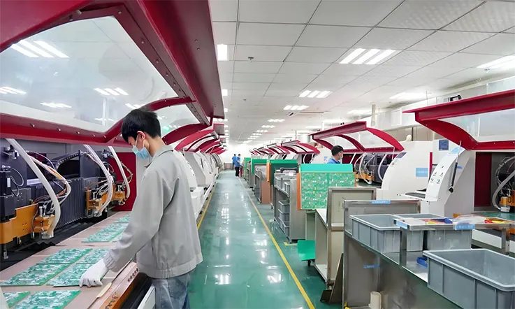
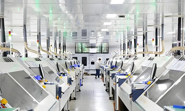
Nelco N4000-7 SI laminates are designed to support stable electrical behavior in applications where high-frequency signal integrity must be maintained. Achieving dependable yields with this low-loss material calls for a manufacturing approach built on practical knowledge and careful process control. With over three decades of experience serving the telecommunications, aerospace, and medical sectors, we recognize how the material responds during pressing, drilling, and final surface treatment—and how each of these steps influences real-world performance in the finished product.
The following steps are refined specifically for Nelco N4000-7 SI PCB manufacturing, based on repeated production success in complex, multilayer stack-ups.
Material Handling, Lay-up, and Vacuum Lamination
Working with Nelco N4000-7 SI demands focused attention from the moment materials enter our facility.
●Strict Environmental Controls: Prepreg sheets, known for their controlled resin flow, are stored in an environment with carefully regulated humidity and temperature—typically kept below 5°C—with efforts made to minimize exposure during the setup process.
●High-Precision Lay-up: During lay-up, the accuracy of core-to-prepreg alignment is what allows the impedance model to translate perfectly to the finished board.
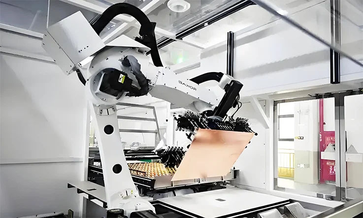
●Targeted Vacuum Lamination:For structures exceeding 10 layers, we apply vacuum lamination to reduce void formation and control resin distribution. The press cycle is precisely adjusted to match the specific resin melt and flow characteristics of this laminate, helping maintain accurate layer alignment and meet the intended dielectric values.
●Customized Lamination Cycles: Custom lamination profiles have been developed and validated to produce repeatable results across multiple production runs, especially for builds involving 5G mmWave, high-speed servers, and medical imaging circuits.
Vacuum Lamination & Storage Process Table:
| Parameter | Control Range / Target | Unit |
| Prepreg Storage Temperature | ≤ 5 | °C |
| Relative Humidity in Storage Area | 30–40 | %RH |
| Lay-up Alignment Tolerance | ±25 | μm |
| Lamination Temperature (Peak) | 185–195 | °C |
| Lamination Pressure | 180–220 | psi |
| Heating Rate | 2–4 | °C/min |
| Vacuum Application Time | ≥ 20 | min (before press) |
| Total Cycle Time (multi-lam) | 90–150 | min |
Drilling, Desmear, and Plated-Through Hole (PTH) Reliability
Drilling precision directly influences the reliability of plated-through holes, especially in high-layer-count Nelco N4000-7 SI builds.
●Optimized Drilling Parameters: Drill parameters are adjusted according to the specific glass-weave style and resin content of the laminate to minimize the risk of resin smear and glass fiber protrusion.
●Two-Step Desmear Process: After drilling, employ a two-step desmear process using both plasma and a solvent-based chemical treatment. This ensures the hole wall is perfectly prepped for copper deposition without damaging the resin system, a process proven effective in preventing over-etching.
●Proven PTH Reliability: Reliability testing on plated-through holes in this laminate has met thermal shock, IST (Interconnect Stress Test), and CAF resistance criteria across more than 500 production lots, demonstrating its robustness for long-term deployment.
Drilling & PTH Performance Table:
| Parameter | Typical Setting / Outcome | Unit |
| Entry/Exit Stack Support Material | FR4 + Aluminum Foil | – |
| Drilling Speed (per laminate type) | 100–130 | krpm |
| Feed Rate | 1.2–1.5 | inch/min |
| Hole Wall Roughness (post-drill) | ≤ 15 | μm |
| Plasma Desmear Time | 8–12 | min |
| Chemical Desmear Temperature | 65–70 | °C |
| Thermal Shock Pass Cycles | ≥ 6 | 288°C |
| IST Stability | Pass > 500 cycles | @ 260°C |
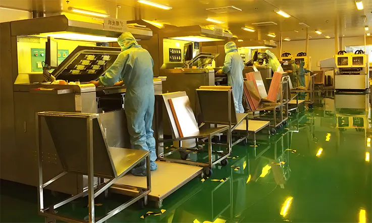
Surface Finishing Techniques: ENIG, OSP, and Immersion Silver
The final surface treatment has a direct bearing on signal launch and contact performance.
●ENIG (Electroless Nickel Immersion Gold): This finish is frequently specified for RF and microwave applications due to its stable contact resistance and high planarity.
●OSP (Organic Solderability Preservative): For designs prioritizing fine-pitch solderability—common in medical devices—OSP is often used to protect the copper during lead-free assembly.
●Immersion Silver: In applications requiring superior signal performance at launch points with minimal loss, immersion silver is a preferred choice.
●Precision Process Control: All three finishes perform well on this laminate, but each requires specific plating bath controls and dwell-time management to avoid pad discoloration or etch-back, particularly when fabricating boards with fine geometries and dense via arrays.
Electrical and Reliability Testing for Nelco N4000-7 SI PCBs
In PCB manufacturing, testing is not an afterthought—it forms a continuous thread throughout every stage of process control. For multilayer PCBs fabricated with Nelco N4000-7 SI, particularly in applications demanding stable signal transmission, electrical and reliability evaluations provide clear evidence of manufacturing precision. From impedance traceability to performance under thermal stress, each test conducted directly indicates how a board will perform once it leaves the production facility.
By aligning processes with established industry testing protocols, engineers and procurement teams gain the confidence needed to move forward across applications such as mmWave base stations, medical scanners, and mission-ready avionics. As a manufacturing partner, the goal is to deliver boards that fulfill design intent and maintain reliable performance under the specific conditions for which they are intended.
Impedance, Insertion Loss, and Return Loss Testing
For high-speed signal integrity PCBs, stable impedance and low-loss performance are baseline expectations. We verify the performance of our Nelco N4000-7 SI boards through the following methods:
●Time Domain Reflectometry (TDR) Testing: Automated TDR equipment is employed on test coupons fabricated alongside every production panel to verify that characteristic impedance meets design specifications.
●S-Parameter Measurements: Insertion loss and return loss at relevant GHz frequencies are measured using a Vector Network Analyzer (VNA) to evaluate overall signal integrity.
●A Reflection of Process Capability: These test results are more than just a compliance check; they are a direct reflection of our ability to hold tight tolerances on dielectric thickness, resin content, and copper geometry.
Thermal Shock and CAF Qualification Standards
High-speed PCBs, especially in defense and telecom infrastructure, frequently undergo aggressive thermal cycling. Validation of Nelco N4000-7 SI’s performance under real-world build conditions is conducted to ensure reliability.
●Thermal Shock Testing: Rigorous thermal shock tests (e.g., multiple cycles from -55°C to +260°C) are conducted in accordance with IPC-TM-650 to validate the board’s structural integrity under extreme temperature changes.
●CAF Resistance Qualification: Testing is performed under high-humidity, high-voltage bias conditions to confirm the board’s resistance to Conductive Anodic Filament (CAF) formation, a failure mode that affects long-term reliability in high-density applications.
●IPC Class III as a Foundation: Especially in HDI or tight-pitch designs, IPC Class III workmanship standards are applied to drilling, desmear, and lamination processes, establishing a foundation for the board to meet long-term reliability tests.
IPC, UL, and ISO Compliance in Our Testing Protocols
Meeting formal compliance requirements is a cornerstone of our quality promise. We provide comprehensive quality assurance for our Nelco N4000-7 SI PCBs.
●IPC Quality Standards: Boards are delivered meeting IPC-A-600 Class 2 or Class 3 quality levels, depending on the end-use application, with full traceability to raw material lots and manufacturing parameters.
●Comprehensive Reporting: Boards are supplied with conformance reports aligned with IPC-6012, documenting details such as impedance deviation, plating thickness, hole-wall integrity, and solderability.
●System and Safety Certifications:For clients in the aerospace and medical sectors, ISO 9001:2015 quality management certification is maintained along with provision of UL94-V0 flame rating documentation.
From insertion loss measurements to micro-section analysis for interconnect reliability, every aspect of testing is integrated into a quality management system based on controlled and repeatable manufacturing practices.
Cost Drivers and Budgeting Tips for Nelco N4000-7 SI Projects

When fabricating with Nelco N4000-7 SI, the overall cost structure reflects a combination of material properties, stack-up configuration, process complexity, and production volume—not simply the laminate price. For procurement engineers and design teams focused on maintaining high-frequency performance, making sound budgeting decisions requires a clear understanding of how these manufacturing factors influence total build cost.
As a manufacturer experienced in high-frequency board builds, we have managed a wide range of N4000-7 SI configurations. Based on this track record, we have outlined how material specifications, design complexity, and sourcing coordination shape the final unit price, and how planning ahead can prevent unnecessary cost accumulation.
Impact of Material Grade and Laminate Thickness on Cost
Cost Drivers:
●Material Specifications: Thicker cores, low-flow prepregs, or the ultra-thin dielectrics used for controlled impedance can meet specific performance goals, but they also increase the difficulty of lamination and registration. This can lead to lower yields and longer production cycles.
●Tight Tolerance Demands: Specifying excessively tight tolerances without a joint review can significantly increase screening, inspection costs, and scrap rates, especially in complex constructions of 8 layers or more.
Budgeting Tips & Our Approach:
●Engage in Early Design for Cost (DFC) Review: Collaborate with our engineers in the initial design phase to review your material choices. We can help you assess the cost impact of different specifications, avoid unnecessary over-engineering, and find the optimal balance between performance and your budget.
●Standardize Where Possible: If feasible, using a manufacturer’s standard, in-stock material specifications for non-critical layers can improve manufacturing efficiency and reduce material overhead.
Volume-Based Pricing and Fabrication Complexity
Cost Drivers:
●Manufacturing Complexity: Each additional lamination cycle (e.g., for HDI boards) or complex feature like back-drilling or stacked microvias directly adds to equipment time, labor, and thermal stress management costs.
●Panel Utilization: Board dimensions and layouts that are not optimized for a standard production panel result in material waste, which directly increases the cost per unit.
Budgeting Tips & Our Approach:
●Optimize for Panelization Early: We can assist you during the early layout stage to plan board dimensions that maximize utilization on our production panels, directly reducing material waste and cost.
●Discuss Process Simplification: Our engineers can work with you to identify alternative design features (e.g., optimizing via types) that have minimal impact on function but can significantly simplify the fabrication process. This is particularly effective for reducing unit costs in mid- to high-volume production.
Sourcing Strategy for Cost-Effective Manufacturing
Cost Drivers:
●Supply Chain Volatility: The lead times and prices for high-performance laminates can fluctuate. A fragmented or last-minute sourcing strategy can easily lead to expedite fees or project delays due to material shortages.
●Order Fragmentation: Small, frequent orders struggle to achieve economies of scale and can keep per-unit setup and administrative costs high.
Budgeting Tips & Our Approach:
●Leverage Stable Procurement Channels: Partnering with a manufacturer that maintains stable procurement channels and an inventory of common materials helps minimize lead-time gaps and reduce supply chain risks.
●Implement Forward-Looking Demand Planning: We welcome the opportunity to work with you to forecast material selection and approximate volumes ahead of time. This allows us to reserve supply and secure more favorable material pricing, protecting both your budget and your project schedule.
●Communicate Your Delivery Cadence: Establishing clear communication on delivery targets, batch sizes, and revision frequency enables a predictable production rhythm. In many cases, a small adjustment to the delivery schedule or minimum order quantity (MOQ) can significantly lower the cost per unit over the full program timeline.
How to Select the Right Manufacturer for Your Nelco N4000-7 SI PCB Project?
Choosing who builds your PCB has a direct impact—not only on functionality, but also on signal quality, process reliability, and confidence in on-time delivery. When working with advanced materials like Nelco N4000-7 SI, the success of your RF or high-speed design hinges on the manufacturer’s understanding of how the material behaves during fabrication—and their ability to translate that insight into alignment with your layout, stack-up strategy, and performance requirements.
At its core, this decision is not just about capability; it’s about trust, process control, and whether your supplier has walked this road many times before, across projects of varying complexity and scale.
Evaluating Manufacturer Capabilities and Certifications
Before engaging a supplier for boards using Nelco N4000-7 SI, it’s worth reviewing their actual build history with this specific material.
●Assess Practical Material Experience: Ask if they have handled applications involving controlled impedance, mixed-dielectric stack-ups, or complex via-in-pad designs using this resin system. Familiarity should come from practical, shop-floor experience, not just datasheets.
●Verify Specialized Equipment: Check if their fabrication equipment supports the process controls required for high-frequency PCBs, such as Laser Direct Imaging (LDI) for fine-line accuracy, precision vacuum lamination for multi-stage press cycles, and AOI systems calibrated for RF board tolerances.
●Look Beyond the Certificate: Certifications like UL, ISO 9001, and IATF 16949 establish foundational standards, but the true difference comes from how these systems are applied by the operators on the production floor. A manufacturer’s real strength is reflected in the thoroughness and care their teams dedicate to every panel in your build—not just in the paperwork.
The Advantages of an Experienced, China-Based Supplier
China remains a manufacturing hub not only for its scale and cost-efficiency but because many factories here have spent over a decade refining their techniques on specialty laminates like Nelco N4000-7 SI. The true differentiator is the ability to translate demanding stack-ups and drill maps into stable, repeatable processes.
●Mature Processes and Supply Chain: Suppliers with experience supporting 5G infrastructure, medical devices, and aerospace platforms typically have laminate inventory on hand and strong partnerships with authorized distributors.
●Expert Engineering Support: Their CAM and front-end engineers usually have a deep understanding of insertion loss targets and dielectric spacing, enabling an effective and direct feedback loop.
●Integrated DFM Services: Many experienced manufacturers in China provide in-house Design for Manufacturability (DFM) services to help adjust trace widths, via dimensions, or copper balancing early on. These adjustments not only stabilize the build but also help control costs.
Questions to Ask Before Placing Your High-Speed PCB Order
Placing an order for a Nelco N4000-7 SI board is different from submitting a basic FR4 build. Here are a few questions worth asking upfront to ensure your supplier is ready for the task:
●Have you built with this exact N4000-7 SI resin code before?
●How do you manage layer-to-layer registration on high-layer-count boards using this laminate?
●What is your experience with low-loss designs that have tight insertion loss tolerances?
●Can you provide impedance simulation reports or measurement data from test coupons?
●What are your drilling capabilities for stacked or back-drilled vias on this substrate?
●Do you have in-stock prepregs and cores available for rapid prototyping or pilot builds?
The answers to these questions reveal not just technical depth but whether the supplier has the infrastructure and people to follow through. When both sides speak the same engineering language—backed by mature processes—moving from concept to production becomes much smoother, avoiding unnecessary iterations and delays.
Supplier Readiness Questionnaire Summary Table:
| Evaluation Question | Ideal Response Example |
| Built N4000-7 SI before? | “Yes, over 100 projects, mostly 12–20 layer RF boards” |
| Layer-to-layer registration strategy? | “Uses X-ray and optical alignment; ±1.5 mil control” |
| Experience with insertion loss-sensitive designs? | “Validated builds with <0.8 dB/in loss @ 28 GHz” |
| Ability to simulate & measure impedance? | “Use Polar SI + TDR test coupons for verification” |
| Drilling capability (back/stacked vias)? | “5 mil laser drill; 10 mil core drilling; no smear” |
| Stock availability of Nelco cores/prepregs? | “Yes, stocked up to 10 resin codes in multiple thicknesses” |
Why JarnisTech is the Reliable Choice for Your Nelco N4000-7 SI PCB Fabrication?
Selecting a manufacturer for your Nelco N4000-7 SI project means choosing a partner for your product’s performance, stability, and delivery reliability. It requires a fabricator who not only understands advanced materials but can also translate that deep knowledge into your success. JarnisTech integrates our proven process controls, transparent communication, and a profound understanding of high-frequency circuits into a complete service designed to ensure your sophisticated design journey is smooth from start to finish.
More Than a Product: A Technical Partnership from Start to Finish
At JarnisTech, technical support is not an add-on; it is central to our partnership model. We ensure your design intent is perfectly realized through:
●Expert DFM and Engineering Support: Our engineering team works with you to review your design, leveraging our experience from hundreds of N4000-7 SI projects. We provide professional guidance on stack-up design, impedance control, and material selection, helping you avoid common pitfalls like Dk/Df value misuse and stack-up mismatches right from the start.
●Responsive Post-Delivery Follow-Up: After we deliver your boards, our support continues. Whether you have questions about assembly or need clarification on test data, we respond promptly to ensure you can move forward successfully with the PCBs we’ve fabricated. This reflects our commitment to long-term partnership, not just a one-time transaction.
Our Commitment to Delivery and Cost: Transparent, Punctual, and Predictable
We understand that time and budget are the twin pillars of your project’s success. JarnisTech protects these pillars with disciplined planning and transparent pricing.
●Dependable Lead Times: Thanks to our stable relationships with Nelco N4000-7 SI material suppliers and our in-house inventory, we offer reliable and competitive lead times. Our efficient production planning ensures every order, from prototype to volume production, is delivered on schedule.
●Clear and Transparent Quotes: Our quotations provide a clear breakdown of costs driven by material choices, process complexity (like back-drilling or sequential lamination), and testing requirements. There are no hidden fees, allowing you to plan your budget with accuracy and confidence.
Our Core Principles: Fast Response and Uncompromising Quality
In the fast-moving electronics industry, speed and quality are not a trade-off; they are requirements that must be met simultaneously.
●A Fast and Accurate Quoting Process: We understand the urgency of your projects. Our professionally trained quoting team can quickly and accurately assess the complexity of your Nelco N4000-7 SI design to provide a detailed and competitive quotation.
●Evidence-Based Quality Assurance: Every batch of boards we deliver has undergone rigorous inspection, including TDR impedance testing, thermal shock testing, and micro-section analysis. We provide not just a circuit board, but a promise of quality backed by real test data, ensuring it performs consistently in high-frequency applications.
Quality Assurance & Testing Table:
| Quality Process | Test Method | Pass Criteria |
| Controlled Impedance Testing | TDR (Time Domain Reflectometry) | ±10% of target impedance |
| Layer Inspection | Cross-Section Analysis | No delamination / resin voids |
| Thermal Reliability | IST + Thermal Shock | >500 cycles @ 260°C |
| High-Speed Signal Validation | Eye Diagram Testing (optional) | Open eye pattern at >20 Gbps |
| Visual and AOI Review | 2D AOI + Manual Microscopy | 100% coverage + IPC Class 3 criteria |
Future Trends in High-Frequency PCB Materials and Laminate Technologies
The landscape of high-frequency PCB manufacturing is being shaped by the ever-increasing demands of modern electronics. Looking ahead beyond 2025, certain material developments and process innovations clearly indicate the future direction for fabricating boards like those built on Nelco N4000-7 SI. As a forward-thinking manufacturer, we are not just observing these trends; we are actively preparing to meet the challenges they present.
The Emergence of Next-Generation Low-Df Substrates
As signal speeds climb into higher realms, ultra-low dissipation factor (Df) substrates will become standard for maintaining signal fidelity.
●The Future Trend: New resin systems with extremely low Df values and superior high-frequency characteristics will become more common. These new materials will demand updated fabrication techniques, particularly for adhesion control, dielectric uniformity, and copper surface treatments.
Our Approach & Preparation:
●We maintain close relationships with upstream material suppliers to gain early access to samples and technical data for emerging materials, which we evaluate internally.
●Our process engineering team is actively researching custom lamination profiles and surface treatment protocols for these new materials to ensure we can continue to deliver tight impedance control and minimal insertion loss as technology evolves.
The Integration of Photonics with PCBs
To meet explosive data transmission demands, the direct integration of photonic components (like optical waveguides) onto PCBs will become more prevalent.
●The Future Trend: Electro-Optical Circuit Boards (EOCBs) will move from concept to larger-scale production. This presents entirely new manufacturing challenges, such as the precision alignment of optical components and managing the compatibility of dissimilar materials (e.g., polymer waveguides and FR-4) during thermal lamination.
Our Approach & Preparation:
●We are investing in precision alignment and lamination technologies capable of handling the different coefficients of thermal expansion (CTE) between mixed materials.
●Our drilling and routing processes are being upgraded to accommodate the extreme precision required for embedded optical channels, ensuring we can deliver compact form factors without compromising dual electrical and optical performance.
Sustainable and Eco-Friendly High-Speed PCB Materials
The growing focus on sustainability across the manufacturing sector is driving the adoption of more eco-conscious materials and processes in PCB production.
●The Future Trend: Demand will continue to grow for high-performance laminates that are recyclable, halogen-free, or use bio-based resins. Integrating these eco-friendly materials into mature manufacturing workflows presents new challenges in compatibility and quality control.
Our Approach & Preparation:
●We are actively evaluating new, high-performance materials that meet environmental standards and are establishing the quality control benchmarks to ensure their reliability and signal integrity are on par with traditional laminates.
●From responsible material sourcing to optimizing waste handling, we are systematically adapting our production processes to support our clients’ environmental goals while holding firm to our commitment to product performance.
FAQ & Nelco N4000-7 SI PCB
1.Q: Can Nelco N4000-7 SI be used in a hybrid stack-up with standard FR-4 materials?
A: Yes, it’s common in hybrid stack-ups to balance cost. Using N4000-7 SI for critical high-speed signal layers while using standard FR-4 for power or non-critical signal layers is a cost-effective strategy.
2.Q: For optimal signal integrity, what type of copper foil is recommended with N4000-7 SI?
A: Very Low Profile (VLP) or Reverse-Treated Foil (RTF) is recommended. Their smoother surfaces reduce high-frequency conductor losses (skin effect), maximizing the material’s performance.
3.Q: Besides high-speed digital circuits, is N4000-7 SI suitable for high-power RF applications?
A: It is optimized for signal integrity, not high power. For applications above several tens of watts, dedicated high-thermal-conductivity RF materials are a better choice.
4.Q: What is the maximum layer count that can be reliably manufactured with N4000-7 SI?
A: We reliably manufacture builds with over 30 layers. Designs exceeding 40 layers require a detailed Design for Manufacturability (DFM) review to ensure reliability.
5.Q: Does a bare N4000-7 SI PCB have a shelf life before assembly?
A: Shelf life depends on the surface finish. ENIG can last up to 12 months, while OSP is typically 6 months. Boards should be stored vacuum-sealed in a climate-controlled environment.
6.Q: Which simulation software provides accurate models for N4000-7 SI?
A: Mainstream tools like Ansys HFSS®, Cadence® Clarity™, and Keysight ADS have accurate models. For best results, calibrate them using a manufacturer’s measured, frequency-dependent Dk/Df data.
7.Q: What are the standard raw material panel sizes for N4000-7 SI, and how does that affect my design?
A: Common panel sizes are 18″ x 24″ or 21″ x 24″. Designing with these in mind improves material utilization and reduces the unit cost.


