
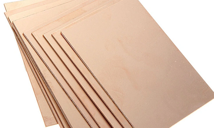
NanYa 175TL laminates represent a category of high-performance materials engineered for advanced printed circuit board (PCB) applications. These materials provide a stable foundation for circuits operating under demanding thermal, electrical, and mechanical conditions. With a high glass transition temperature (Tg) of 175°C, they offer exceptional stability during lead-free soldering and in high-temperature operating environments. Their formulation balances thermal resistance, electrical insulation, and mechanical robustness, making them a preferred substrate for complex, multilayer designs where standard FR-4 materials fall short. This guide provides a comprehensive technical breakdown of NanYa 175TL’s properties, advanced fabrication considerations, and its strategic positioning within the competitive landscape of high-performance substrates.
Core Properties of NanYa 175TL: A Technical Breakdown
Understanding the fundamental characteristics of NanYa 175TL is the first step in leveraging its full potential. The material’s composition, a specialized epoxy resin system reinforced with woven glass fabric, gives rise to a unique combination of thermal, electrical, and mechanical attributes.
Superior Thermal Performance
The ability to manage heat defines NanYa 175TL, directly impacting the reliability and lifespan of electronic assemblies.
● High Glass Transition Temperature (Tg): A nominal Tg of 175°C ensures the material maintains structural rigidity and dimensional stability during high-temperature assembly processes like reflow soldering and in applications with significant power dissipation. This attribute mitigates risks such as warping and delamination.
● High Decomposition Temperature (Td): A Td typically exceeding 340°C provides a substantial safety margin, ensuring the material does not chemically break down under extreme thermal spikes. This is fundamental for assembly survival in harsh environments.
● Low Coefficient of Thermal Expansion (CTE): The material exhibits a low Z-axis CTE, typically around 50 ppm/°C below Tg. This minimizes stress on plated through-holes (PTHs) and microvias during thermal cycling, greatly enhancing the long-term reliability of multilayer boards.
Thermal Properties of NanYa 175TL:
| Parameter | Typical Value | Unit | Notes |
| Glass Transition Temperature (Tg) | 175 | °C | Measured by DSC or TMA |
| Decomposition Temperature (Td) | ≥ 340 | °C | At 5% weight loss (TGA) |
| Z-Axis CTE (Below Tg) | ~50 | ppm/°C | Typical for multilayer reliability |
| Z-Axis CTE (Above Tg) | ~250 | ppm/°C | |
| T260 / T288 | >60 / >10 | Minutes | Time to delamination at 260°C / 288°C |
Advanced Electrical Characteristics
For high-speed digital and high-frequency analog circuits, the substrate’s electrical properties directly influence signal integrity. NanYa 175TL is formulated for predictable electrical performance.
● Stable Dielectric Constant (Dk): The material maintains a stable Dk of approximately 4.2 at 1 GHz across a wide range of frequencies and operating temperatures. This uniformity is fundamental for achieving accurate impedance control in transmission lines.
● Low Dissipation Factor (Df): With a dissipation factor (loss tangent) of ≤ 0.018 at 1 GHz, NanYa 175TL minimizes signal energy loss, especially in high-frequency applications. This results in better signal-to-noise ratios and allows for longer trace lengths.
● High Volume and Surface Resistivity: Excellent insulation properties prevent current leakage between conductive layers and traces, a necessity for high-density and high-voltage applications.
Electrical Properties of NanYa 175TL:
| Parameter | Typical Value | Unit | Test Condition |
| Dielectric Constant (Dk) | ~4.2 | — | At 1 GHz |
| Dissipation Factor (Df) | ≤ 0.018 | — | At 1 GHz |
| Volume Resistivity | ≥ 1.0 × 10¹⁰ | MΩ·cm | After moisture conditioning |
| Surface Resistivity | ≥ 1.0 × 10⁹ | MΩ | After moisture conditioning |
| Electric Strength | ≥ 40 | kV/mm | ASTM D149 |
Robust Mechanical Strength and Durability
The mechanical resilience of NanYa 175TL ensures PCBs withstand the rigors of fabrication, assembly, and end-use operation.
● High Peel Strength: The material demonstrates strong adhesion between the copper foil and dielectric substrate (typically ≥1.5 N/mm), reducing the likelihood of trace lifting during thermal stress or physical rework.
● Excellent Flexural Strength: The woven glass reinforcement provides high flexural strength, preventing fractures or cracking when the board is subjected to vibration, shock, or other mechanical stresses.
● Dimensional Stability: NanYa 175TL shows minimal shrinkage or expansion during etching and lamination, a prerequisite for achieving precise layer-to-layer registration in complex multilayer PCBs.
Mechanical Properties of NanYa 175TL:
| Parameter | Typical Value | Unit | Notes |
| Peel Strength (1 oz Cu) | ≥ 1.5 | N/mm | After thermal stress |
| Flexural Strength (Lengthwise/Crosswise) | 600 / 500 | MPa | ASTM D790 |
| Dimensional Stability | ≤ 0.05 | % | After thermal exposure or processing |
| Young’s Modulus | ~22,000 | MPa | Indicative of stiffness |
Positioning NanYa 175TL: A Global Brand-to-Brand Analysis
Selecting the ideal high-performance laminate requires a nuanced understanding of how different materials behave during fabrication and perform in specific applications. This direct, brand-to-brand analysis provides a strategic perspective for a project’s technical and commercial goals.
vs. Isola (FR408HR / IS410): The High-Speed Digital Arena
● Market Positioning: Isola’s FR408HR and IS410 are widely recognized benchmarks in the high-speed digital space for networking and server applications. They are direct competitors to NanYa 175TL, where performance is centered on signal integrity for data rates exceeding 25 Gb/s.
● Performance Nuances: While FR408HR may exhibit a slightly lower dissipation factor on paper, NanYa 175TL demonstrates exceptional Dk stability across a broad frequency spectrum and varying environmental conditions. From a fabrication standpoint, NanYa 175TL often presents a wider processing window during lamination, a deciding factor for improving yield on boards with very high layer counts or complex constructions.
● Fabrication and Cost Verdict: Both materials require meticulous process control. However, NanYa 175TL frequently offers a more accessible supply chain and favorable cost structure, providing a compelling total cost of ownership. It delivers performance functionally indistinguishable from its Isola counterparts for many designs, making it a powerful, economically sound choice.
NanYa 175TL vs. Isola FR408HR / IS410:
| Property | NanYa 175TL | FR408HR (Isola) | IS410 (Isola) |
| Dielectric Constant (Dk @1GHz) | ~4.2 | ~3.66 | ~4.0 |
| Dissipation Factor (Df @1GHz) | ≤ 0.018 | ≤ 0.009 | ≤ 0.015 |
| Tg (DSC) | 175°C | 180°C | 180°C |
| Td (5% weight loss) | >340 | ~325 | ~340 |
vs. Shengyi (S1000-2 / S1170G): The High-Volume, High-Reliability Battle
● Market Positioning: Shengyi is a dominant force, offering reliable materials that balance performance and cost-effectiveness. Their S1000-2 and S1170G laminates are direct competitors to NanYa 175TL in demanding sectors like automotive, industrial, and high-end consumer electronics.
● Reliability and Repeatability: Both NanYa and Shengyi products exhibit excellent thermal cycling performance and CAF resistance. The differentiator is often lot-to-lot uniformity in mass fabrication. Through stringent incoming quality control, including dielectric analysis, NanYa 175TL has demonstrated exceptional batch-to-batch uniformity in its electrical properties, a foundational element for repeatable impedance control.
● Fabrication and Supply Verdict: A deep relationship with the NanYa supply chain ensures stable material access and predictable lead times, a significant logistical advantage in high-volume manufacturing. While Shengyi offers a formidable product, the choice can be guided by supply chain dynamics and specific reliability metrics.
NanYa 175TL vs. Shengyi S1000-2 / S1170G:
| Property | NanYa 175TL | S1000-2 (Shengyi) | S1170G (Shengyi) |
| Tg (DSC) | 175°C | 170°C | 170°C |
| Td (5% loss) | >340 | ~330 | ~330 |
| Dk (1GHz) | ~4.2 | ~4.4 | ~4.3 |
| Df (1GHz) | ≤ 0.018 | ≤ 0.020 | ≤ 0.019 |
vs. Rogers (RO4350B): A Matter of Application, Not Direct Competition
● Market Positioning: This comparison showcases technical expertise by preventing material misapplication. Rogers RO4350B is a ceramic-filled hydrocarbon laminate, not an epoxy system. It is designed explicitly for RF and microwave applications (typically >3 GHz).
● The Electrical Divide: The performance difference is stark. RO4350B’s dissipation factor (~0.0037 @ 10 GHz) is an order of magnitude lower than NanYa 175TL’s (~0.017 @ 10 GHz). For a 5G antenna or automotive radar, RO4350B is appropriate. For a server motherboard’s PCIe Gen5 lanes, NanYa 175TL provides sufficient performance at a fraction of the cost.
● Fabrication Verdict: The materials are not interchangeable. Fabrication capability is demonstrated by creating hybrid stack-ups, expertly bonding layers of Rogers material with layers of NanYa 175TL. This requires deep knowledge of managing disparate CTE values and lamination profiles in a single cycle.
NanYa 175TL vs. Rogers RO4350B:
| Property | NanYa 175TL | RO4350B (Rogers) |
| Dielectric Constant (Dk @10GHz) | ~4.2 | ~3.48 |
| Dissipation Factor (Df @10GHz) | ~0.017 | ~0.0037 |
| Tg (DSC) | 175°C | N/A (thermoset) |
| Td (5% loss) | >340 | ~390 |
| RF Frequency Suitability | Moderate (≤6GHz) | Excellent (>3GHz) |
vs. Ventec (VT-47 / VT-4B5): The Pursuit of Extreme Reliability
● Market Positioning: Ventec is a strong competitor, with its VT-47 and VT-4B5 materials often specified where thermal reliability and durability are primary concerns, such as in demanding industrial and automotive systems.
● Performance Focus: Both NanYa 175TL and Ventec’s offerings excel in thermal stress tests. Peel strength and mechanical robustness are also comparable. Subtle differences can emerge in process interactions. For instance, process validation has shown NanYa 175TL’s resin chemistry can offer a more receptive surface for palladium adhesion during the electroless copper step, enhancing long-term PTH integrity.
● Fabrication and Certification Verdict: Both brands carry extensive industry certifications. The decision can depend on customer approvals or regional supply preferences. Maintaining expertise and optimized processing parameters for both material families provides the flexibility to choose the best-fit material for a design.
NanYa 175TL vs. Ventec VT-47 / VT-4B5:
| Property | NanYa 175TL | VT-47 (Ventec) | VT-4B5 (Ventec) |
| Tg (DSC) | 175°C | 180°C | 185°C |
| Td (5% loss) | >340 | ~340 | ~345 |
| Peel Strength (1 oz Cu) | ≥1.5 | ≥1.5 | ≥1.5 |
| Df @ 1GHz | ≤0.018 | ~0.017 | ~0.015 |
The Physics of Signal Integrity in NanYa 175TL Substrates
Achieving high-speed signal integrity is an exercise in applied physics, where the substrate’s properties and the circuit’s physical geometry interact. NanYa 175TL provides a stable canvas, but realizing its potential requires understanding the underlying principles.
Controlling Impedance Beyond the Datasheet
● Geometry and Material Interaction: A trace’s impedance depends on its width, the distance from a reference plane, and the dielectric constant (Dk) of the surrounding material. For outer layers (microstrip), the presence of solder mask must also be factored into the calculation. Inner layers (stripline), being enclosed between reference planes, provide a more controlled electromagnetic environment. NanYa 175TL’s stable Dk across frequency ranges makes signal modeling more predictable, but accurate fabrication is required to preserve the intended trace dimensions and spacing.
● The Fiber Weave Effect: At multi-gigabit frequencies, the woven glass reinforcement can introduce localized Dk variations. This “fiber weave effect” can cause slight impedance fluctuations, leading to increased bit error rates. Mitigation strategies include routing traces at a slight angle to the weave axis or selecting flatter glass styles, both addressed during advanced DFM review.
Crosstalk Mitigation in High-Density Routing
● NEXT/FEXT: When signal traces run parallel, the electromagnetic field from one (the aggressor) induces noise voltage in the other (the victim). This crosstalk is directly proportional to the coupling length and inversely proportional to the distance between traces. NanYa 175TL’s stable dielectrics allow for accurate modeling of this coupling.
● Physical Isolation Techniques: Fabrication processes enable solutions to combat crosstalk, such as routing sensitive traces with increased spacing or inserting a grounded “guard trace” between them. In stripline configurations, the inherent ground planes provide excellent shielding, making it the preferred routing strategy for sensitive, high-speed nets.
Managing Frequency-Dependent Losses
● Dielectric and Conductor Losses: Total signal loss (insertion loss) has two components. Dielectric loss is energy absorption by the substrate, increasing with frequency and the material’s Df. NanYa 175TL’s low Df minimizes this. Conductor loss is due to the skin effect (current flowing on the conductor’s surface at high frequencies) and copper resistance.
● The Role of Copper Surface Roughness: A rough copper foil surface increases the path length for high-frequency current, increasing conductor loss. Advanced fabrication uses NanYa 175TL with very low-profile (VLP) copper foils and chemical processes that minimize micro-etching. This preserves a smooth conductor surface, a necessity for maintaining open eye diagrams in 28 Gb/s, 56 Gb/s, and faster signaling environments.
Mastering Interconnects: Advanced Drilling and Plating for NanYa 175TL
The long-term reliability of a complex PCB depends on the quality of its vertical interconnects—the plated through-holes and microvias. Fabricating these structures on NanYa 175TL is a science, requiring specialized equipment and an empirical understanding of the material’s behavior under stress.
Controlling Drill Wander and High Aspect Ratios
● The High Aspect Ratio Challenge: In thick multilayer boards, drilling small-diameter holes results in a high aspect ratio (depth/diameter > 15:1). The primary challenge is “drill wander,” where the bit deviates from a vertical path, leading to misregistration with inner layer pads and compromising connectivity.
● Advanced Mitigation Strategies: To combat drill wander, high-precision drilling machines with excellent Z-axis control are used alongside a “peck drilling” cycle to clear debris and reduce stress. Specialized entry and exit materials guide the drill bit precisely. The inherent rigidity of the NanYa 175TL laminate also helps resist drill wander.
Laser Drilling Microvias: CO2 vs. UV Lasers
● Laser Selection for HDI: For High-Density Interconnect (HDI) structures, microvias are created with lasers. A CO2 laser is effective at ablating the NanYa 175TL epoxy resin but is stopped by copper foil, making it ideal for creating blind vias.
● UV Laser for Precision: When drilling through copper and dielectric, or for via diameters <75μm, a UV laser is often employed due to its shorter wavelength and higher precision. Hybrid laser systems combine the speed of a CO2 laser with the precision of a UV laser, allowing for the optimal method for each specific via structure.
The Science of High Throwing Power Plating
● Uniform Plating in Deep Holes: “Throwing power” describes an electroplating bath’s ability to deposit a uniform thickness of copper inside a hole. Poor throwing power results in thin copper in the center, a weak point that can fail under thermal stress.
● Advanced Plating Control: Achieving high throwing power, especially in high-aspect-ratio holes, utilizes advanced DC and pulse-plating rectifiers to precisely modulate current. This, combined with sophisticated chemical solutions containing proprietary additives, promotes even ion distribution deep inside the holes. Vigorous fluid agitation ensures a constant supply of fresh ions, resulting in a robust, reliable plated through-hole.
Pushing the Limits: HDI and Advanced Structures with NanYa 175TL
Fabrication capability is demonstrated by executing complex designs. Using stable platforms like NanYa 175TL enables next-generation electronics.
Mastering Stacked Microvia and Any-Layer HDI Fabrication
● High-Density Interconnects (HDI): NanYa 175TL’s smooth surface and dimensional stability make it a reliable base for HDI designs, which use laser-drilled microvias to allow for much denser component placement and routing.
● Stacked Microvias (e.g., 1+N+1, 2+N+2): A perfected process allows for stacking microvias on top of each other. This requires multiple sequential lamination, drilling, and plating cycles. Each microvia is filled with conductive material and planarized before the next is created. The thermal stability of NanYa 175TL is a prerequisite to survive these repeated thermal excursions.
● Any-Layer HDI: This represents the pinnacle of HDI, where any layer can be connected to any other through microvias. It provides ultimate routing density but is the most challenging to manufacture. Advanced process control and registration systems are capable of producing these complex structures with high yield.
The Precision of Back-Drilling for Signal Purity
● The Stub Problem: In a high-speed signal path, the unused portion of a plated through-hole barrel acts as an antenna stub, which can resonate and cause severe signal reflections, degrading signal integrity.
● The Back-Drilling Solution: A controlled-depth drilling process, also known as back-drilling, removes the unused stub. A slightly larger drill bit carefully drills back into the hole, stopping just short of the last signal layer connection.
● Precision Operation: This is a high-precision process. Automated drilling equipment with Z-axis control ensures it is performed with micron-level accuracy, dramatically improving signal performance for data rates above 5 Gb/s.
Complex Hybrid Constructions: Integrating Diverse Materials
● Combining Performance: Some designs require both the RF performance of a material like Rogers and the robust, cost-effective performance of NanYa 175TL for digital sections.
● Fabrication Challenge: Joining different materials in one stack-up is exceptionally difficult. Each material has a different CTE and reacts differently to lamination, creating immense internal stress that can lead to delamination or warping.
● Advanced Lamination Expertise: Proprietary lamination profiles and surface preparation techniques are used to successfully fabricate these complex hybrid boards. By carefully managing the lamination cycle and material interactions, a single, reliable PCB can be created.
Advanced Thermal Management Solutions for NanYa 175TL-Based PCBs
While NanYa 175TL has superior thermal properties, modern power electronics often require thermal management strategies implemented at the board level. Advanced techniques integrated into the manufacturing process actively draw heat away from sensitive components.
Heavy Copper Plating for High-Current Applications
● High Current Capacity: Applications in automotive, industrial, and power supply design often require current capacities beyond standard 1 or 2 oz copper. Fabrication capabilities exist for NanYa 175TL boards with heavy copper weights from 3 oz to 10 oz or more.
● Process Control: Fabricating heavy copper boards is a specialized skill requiring precise plating control to ensure uniform thickness across the panel. The stability of NanYa 175TL is beneficial, minimizing board distortion during prolonged plating cycles.
● Heat Dissipation: Heavy copper traces and planes act as excellent heat spreaders, pulling thermal energy away from high-power components and distributing it over a larger area, lowering peak component temperatures.
Heavy Copper PCB Capabilities:
| Parameter | Typical Value | Unit | Notes |
| Copper Thickness | 3 – 10+ | oz/ft² | May vary by fab capability |
| Resulting Copper Thickness | 105 – 350+ | μm | After plating |
| Max Continuous Current | Up to 60 | A | Depends on trace width and copper weight |
| Thermal Conductivity (Cu) | ~385 | W/m·K | Effective spreading of localized heat |
| Tolerance (Thickness) | ±10% | — | Requires tight plating process control |
Integration of Embedded Coins and Metal Cores
● Localized Heat Spreading: For extreme, concentrated thermal challenges, an embedded coin is an effective solution. A solid copper or aluminum coin is embedded directly into a cutout in the PCB, flush with the surface. The component is then mounted directly onto the coin.
● Fabrication Complexity: The process is intricate, requiring precision CNC machining of the PCB and coin, followed by a specialized bonding process during lamination. Advanced registration and lamination systems manage the CTE mismatch between the metal coin and the NanYa 175TL laminate.
● Metal Core PCBs (MCPCB): For applications where the entire board must dissipate heat, a metal core PCB is used. The circuit is built on a thin layer of NanYa 175TL laminate bonded to a thick aluminum or copper base plate. This construction transforms the entire board into a heat sink.
Embedded Coin / Metal Core Parameters:
| Parameter | Typical Value | Unit |
| Coin Material | Copper / Aluminum | — |
| Coin Thickness | 1 – 3 | mm |
| Coin Flatness Tolerance | ±25 | μm |
| Base Metal for MCPCB | Aluminum / Copper | — |
| Dielectric Thickness on MCPCB | 75 – 150 | μm |
| Thermal Conductivity (Base) | 200+ (Al), 385+ (Cu) | W/m·K |
Design and Fabrication of Thermal Vias
● Thermal Pathway Creation: Thermal vias are plated through-holes in a dense array under a component’s thermal pad. Their purpose is to create a low-resistance thermal path from the top of the board to internal planes or the bottom side.
● Via-in-Pad Plated Over (VIPPO): For maximum thermal transfer, the VIPPO technique is used. Vias are drilled directly into the component’s solder pads, filled with a thermally conductive epoxy, and then plated over with copper, creating a flat, solderable surface for the most direct thermal path.
● Optimized Arrays: The effectiveness of a thermal via array depends on via diameter, plating thickness, and array density. Design guidance on optimizing these parameters helps achieve a target thermal resistance, turning internal copper planes into an effective heat sink.
Thermal Via and VIPPO Specifications:
| Parameter | Typical Value | Unit |
| Via Diameter | 0.2 – 0.5 | mm |
| Finished Hole Plating Thickness | ≥ 25 | μm |
| Via Array Pitch | 0.5 – 1.0 | mm |
| Thermal Conductivity (VIPPO Fill) | ~3 – 6 | W/m·K |
| Max Thermal Transfer Area | Application specific | mm² |
| Surface Planarity (VIPPO) | ≤ ±15 | μm |
Navigating CAF Resistance: Material Science and Process Control
Conductive Anodic Filament (CAF) formation is a failure mode where an electrochemical migration occurs along the glass-resin interface, creating a conductive path between two biased features. Preventing CAF is a primary objective for high-reliability applications.
The Mechanism of CAF Formation
● Necessary Conditions: CAF requires a path (the glass-resin interface), an electrical bias, and an electrolyte (typically moisture). When met, copper ions from the anode migrate along the fiber, eventually forming a short circuit.
● NanYa 175TL’s Inherent Resistance: The resin system in NanYa 175TL is formulated for high chemical stability and low moisture absorption. The strong bond between the epoxy and glass fibers leaves fewer pathways for moisture, giving the material high intrinsic resistance to CAF.
Process Controls to Eliminate CAF Risk
● Drilling and Desmear Optimization: The drilling process can create damage sites along the hole wall. Using sharp drill bits and optimized feed/speed rates for NanYa 175TL minimizes this stress. A subsequent chemical desmear process cleans the hole wall, but an overly aggressive process can expose more glass fibers. Titrating this process for the specific material is a feature of a high-reliability fabrication line.
● Superior Hole Wall Preparation: Before plating, the hole wall must be clean and properly texturized to promote strong copper adhesion. A robust cleaning cycle ensures no contaminants are left. A strong, uniform electroless copper deposition provides a seamless barrier, further sealing the glass-resin interface from moisture ingress.
Micro-Section Analysis: A Window into Interconnect Reliability
For ultimate assurance of interconnect quality, nothing replaces the visual evidence from a micro-section analysis. This destructive test involves cutting a coupon from a production panel, encapsulating it in epoxy, and polishing it to reveal a cross-section of plated holes, providing an unfiltered view of fabrication quality.
Verifying Plated Through-Hole (PTH) Integrity
● Plating Uniformity: A quality micro-section reveals uniform copper plating from top to bottom. The “throwing power” is quantified by the ratio of the center barrel thickness to the surface thickness; >90% is indicative of a superior process. Any thinning suggests a potential failure point.
● Registration and Annular Ring: The analysis confirms the drill was perfectly centered on the inner layer pads, with a sufficient and uniform annular ring visible on all layers. The absence of drill wander or misregistration is a direct measure of process precision.
● Hole Wall Quality: The micro-section reveals the copper-laminate interface. A perfect interface shows strong adhesion with no voids, delamination, or “negative etchback.” This smooth, well-bonded interface is a testament to a well-controlled desmear and plating preparation process.
Inspecting HDI Microvia Structures
● Via Formation: For laser-drilled microvias, the section confirms the via’s shape, depth, and the quality of the bottom interface. An ideal blind via has a clean, flat bottom, showing the laser stopped cleanly on the target pad without damage.
● Copper Fill and Planarity: In stacked designs, the fill of lower vias is examined. It should be solid, void-free conductive material. The surface must be planarized (flattened) before the next via is built on top. The micro-section verifies this planarity, which is a necessity for reliable connections.
Precision Masking and Marking on High-Density Boards
The solder mask and legend (silkscreen) are functional components that impact assembly, performance, and reliability, especially on high-density PCBs. On a premium NanYa 175TL board, the precision of these layers is a testament to a facility’s attention to detail.
1.Achieving Fine Solder Mask Dams
● The Solder Bridge Problem: On fine-pitch components (e.g., 0.4mm pitch BGAs), the space between pads is minuscule. The solder mask must form a thin, durable “dam” in this space. If the dam is broken or missing, solder can flow between pads, creating a short circuit.
● The Photolithography Process: Liquid Photoimageable (LPI) solder mask is applied and then hardened by exposure to UV light through a phototool. To create fine dams, high-resolution phototools and highly collimated UV light sources are used. Collimated light prevents scattering that would undercut the dam shape. NanYa 175TL’s dimensional stability ensures perfect registration of the mask layer.
2.Controlling Solder Mask Thickness
● Impact on Impedance: For controlled impedance traces on outer layers, the solder mask thickness over the trace affects the final impedance value. Automated coating equipment applies the LPI mask with controlled, uniform thickness, ensuring the final impedance matches the design model.
● Impact on Assembly: An irregular solder mask surface can lead to component placement problems, such as “tombstoning” of small passive devices or unreliable solder joints under large BGAs. Keeping tight control over mask thickness helps improve assembly success rates and reduces the chance of rework.
3.High-Resolution Legend Printing via Direct Inkjet
● The Inkjet Advantage: Traditional screen printing struggles with fine lines and small text. High-resolution direct inkjet printing technology sprays tiny droplets of ink directly onto the board with extreme precision. This allows for legible text small enough to fit between fine-pitch pads and enables the printing of machine-readable 2D barcodes for unparalleled traceability.
Advanced Quality Assurance Protocols for NanYa 175TL Boards
A multi-layered quality assurance methodology ensures every NanYa 175TL PCB delivered is verifiably flawless.
● Multi-Stage Automated Optical Inspection (AOI): Every inner layer is scanned after etching for subtle defects. After lamination, X-ray inspection verifies precise layer-to-layer registration. A final AOI scan after outer layer processing checks for surface defects and solder mask registration.
● Comprehensive Electrical Testing: For prototypes, flying probe testing provides a fixtureless method to test every net. For high-volume fabrication, custom bed-of-nails fixtures allow for simultaneous testing of all nets, ensuring high throughput. Every board is tested.
● Impedance Control Verification: Test coupons on every panel are subjected to Time-Domain Reflectometry (TDR) measurements to provide empirical proof that traces meet the required impedance values within tolerance.
● Material and Process Traceability: A barcode is assigned to each raw laminate sheet and scanned at every major processing step, creating a complete digital history. Meticulous records link finished PCBs to specific material lots and process chemistries. A Certificate of Conformance (CofC) accompanies every shipment.
The Economics of High-Performance: Total Cost of Ownership (TCO)
Focusing solely on the upfront PCB cost is misleading. TCO, which accounts for yield, assembly success, field reliability, and time-to-market, presents a more insightful metric. Through the lens of TCO, choosing a premium material like NanYa 175TL from a top-tier facility presents a compelling financial case.
● Yield-Based Analysis: The stability and robustness of NanYa 175TL lead to higher fabrication yields, especially for complex boards. Its high Tg drastically reduces assembly-line failures (e.g., pad lift, PTH cracks), saving significant costs associated with rework and scrap.
● The Financial Impact of Long-Term Reliability: A primary TCO driver is the cost of field failures. The enhanced CAF resistance and thermal cycling endurance of well-fabricated NanYa 175TL boards translate to a longer, more reliable product life, safeguarding brand reputation and the bottom line. For equipment with expected service lives of 10-15 years, this is not optional.
● Reducing Development Cycles: Comprehensive DFM feedback and process control expertise increase the probability of first-pass success, avoiding costly board respins and accelerating time-to-market.
Application Suitability Across Demanding Industries
NanYa 175TL’s balanced profile makes it a versatile choice for a wide array of high-performance applications.
● Telecommunications and 5G Infrastructure: Used in power amplifiers, filters, and backplanes for base stations. Ideal for high-density line cards in network switches and routers.
● Automotive and EV Systems: Suitable for Engine Control Units (ECUs), powertrain controls, and ADAS modules for radar and camera systems processing high-speed data.
● Industrial Automation and Medical Devices: Provides robustness for Programmable Logic Controllers (PLCs). In medical devices like MRI scanners, its low loss contributes to clean signal acquisition.
Handling and Storage Protocols for NanYa 175TL
Adherence to proper handling and storage is necessary to preserve material properties.
● Environmental Controls: Store laminates in a climate-controlled environment (20-25°C, <50% RH) in original light-blocking packaging.
● Contamination Prevention: Handle laminates with clean, lint-free gloves. Keep materials sealed until use.
● Long-Term Storage: Store panels vertically to prevent warping. Implement a First-In, First-Out (FIFO) system. A pre-bake cycle is recommended for material stored for an extended period to drive out absorbed moisture.
Frequently Asked Questions (FAQ)
1.When should a design move from standard FR-4 to NanYa 175TL?
An upgrade is recommended for applications with high operating temperatures (>130°C), multiple lead-free assembly cycles, high layer counts (>8), or demanding thermal reliability where FR-4 may exhibit warping, delamination, or PTH failure.
2.How is the quality of these advanced boards verified?
Through a multi-stage process: TDR testing for impedance, AOI and X-ray for physical integrity, 100% electrical testing for connectivity, and full batch traceability, often supported by micro-section analysis.
3.What is the main application difference between NanYa 175TL and an RF material like Rogers?
They serve distinct purposes. NanYa 175TL is optimized for high-speed digital circuits and power systems. Rogers materials are specialized for RF/microwave frequencies where extremely low signal loss is the primary requirement.
4.Can complex HDI designs be fabricated using NanYa 175TL?
Yes. Specialized facilities have the equipment and processes for complex HDI fabrication with NanYa 175TL, including stacked microvias and any-layer interconnects, which leverage the material’s excellent stability.
Fabrication Spotlight: JarnisTech’s Capabilities with High-Performance Materials
JarnisTech translates complex engineering requirements into tangible, high-reliability circuit boards. The approach is built on a foundation of four key pillars, ensuring that the full potential of advanced substrates like NanYa 175TL is realized for every client project.
1.Advanced Technological Proficiency:
Expertise extends to the most demanding fabrication processes, including any-layer HDI, stacked microvias, controlled-depth back-drilling, and heavy copper plating. This ensures that even the most complex designs are manufactured with precision, maximizing density and performance.
2.Strategic Cost and Value Management:
The focus is on delivering superior value through an optimized Total Cost of Ownership (TCO). This is achieved via intelligent panelization to maximize material utilization, high-yield manufacturing processes to minimize scrap, and proactive guidance to prevent costly design respins.
3.Proactive Supply Chain and Lead Time Control:
To address market volatility, a robust supply chain strategy is in place. This includes maintaining a strategic inventory of critical high-performance materials like NanYa 175TL, fostering deep relationships with material suppliers, and providing data-driven recommendations for qualified alternatives to accelerate project timelines.
4.Collaborative Client and Engineering Support:
Beyond fabrication, a partnership model provides comprehensive support. This includes direct access to engineering expertise for stack-up design and material selection, complemented by rigorous Design for Manufacturability (DFM) analysis on every order to identify and resolve potential issues before manufacturing begins.
Final Words: From Superior Material to Flawless Product
NanYa 175TL PCB material provides a powerful substrate for creating robust, high-performance electronics. Its superior thermal stability, predictable electrical properties, and mechanical durability offer a distinct advantage for complex designs in demanding industries.
However, the full potential of this advanced material is only realized when paired with a fabrication facility that matches its caliber. Success is forged in the details of manufacturing: the micron-level precision of a back-drilling operation, the validated purity of a plating bath, the verified integrity of a microvia fill, and the certainty of a well-managed supply chain. These are the elements that transform a superior material into a flawless final product. Specialization in high-performance PCB fabrication ensures that your specific design intent for a demanding application is translated into a verifiably flawless and reliable final product.


