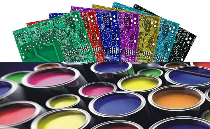
Carbon ink is a type of ink that contains conductive carbon particles, typically in the form of carbon black, mixed with a binder material. The carbon black particles are small and form a dense and continuous network, making the ink electrically conductive.
When applied to a non-conductive substrate such as paper, plastic, or even a PCB substrate, the carbon ink creates a conductive pathway or trace. The ink adheres to the substrate and dries, forming a solid and consistent line of conductive material.
In the case of PCBs, the carbon ink is printed onto the substrate using various printing methods such as screen printing or inkjet printing. The carbon ink traces replace the traditionally used copper traces on the PCB, forming the electrical connections between components. Carbon ink is useful for creating flexible circuits, as it can be applied to a variety of substrates, allowing for more design flexibility while maintaining electrical conductivity.
What Is Conductive Carbon Ink?
Conductive carbon ink is a type of ink that contains carbon particles dispersed in a conductive polymer matrix or solvent. It is used in various applications, including printed circuit board fabrication, membrane switches, sensors, and other electronic components. When applied, the ink can create conductive traces, electrodes, and circuits on the surface of a substrate, enabling the flow of electrical current.
Carbon ink is preferred over traditional metals in certain applications due to its flexibility, low cost, and ease of application. It is also resistant to corrosion and can withstand extreme temperatures, making it suitable for use in harsh environments.
What Is Conductive Carbon Ink PCB ?
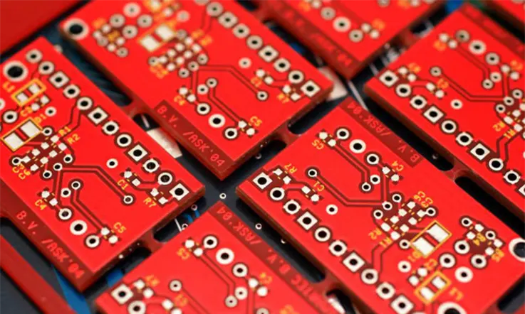
Conductive Carbon Ink PCB, also known as CCI PCB, is a type of printed circuit board that utilizes carbon inks to create conductive traces and pathways. These carbon inks are typically made of a mixture of carbon particles and a binding agent and can be printed onto a non-conductive substrate to form the circuits.
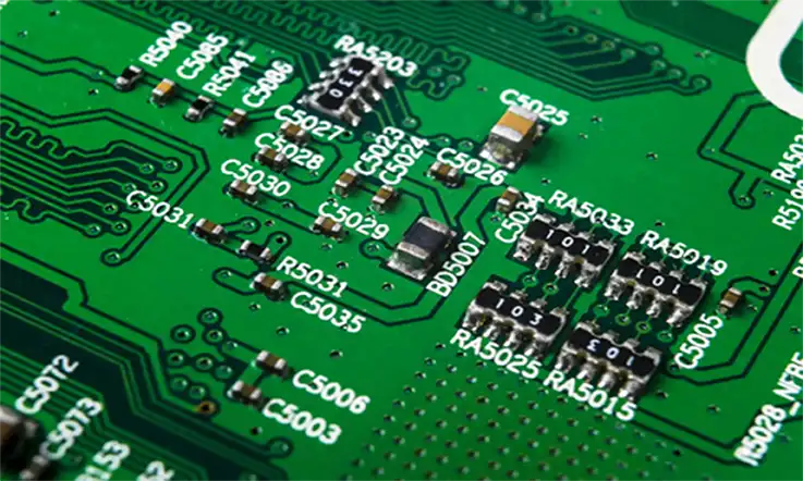
As we know, Carbon ink, a thermally setting conductive carbon paste, is frequently utilized in the assembly of printed circuit boards (PCBs). This ink can be printed via silkscreen methods on a PCB board, connecting neighboring copper features to create a conductor between traces or between traces and components. The cured carbon ink layer transforms into a thick protective film with some resistance which is commonly referred to as Carbon Thick Film PCB or Printed Carbon Resistors (PCR).
The term “carbon paste” may also be utilized to refer to conductive carbon ink, and it can be employed for printing on a wide variety of base materials including FR-4, PTFE, metal cores, and polyimide, which are utilized in rigid PCBs, flex circuits, and rigid-flex boards.
Printing Process of Carbon Ink PCB
● Resistance tolerance control.
The manufacturing process for conductive carbon ink PCBs is similar to that of silver ink PCBs, but there are some differences to note. During operation, gloves must be worn for safety purposes. It is necessary to adjust screen-printing speed and ink suction pressure to achieve optimal printing results, requiring careful testing. The screen stencil, scraper, and carbon oil must meet the specific requirements outlined by the MI engineer.
● Prior to use, it is essential to ensure that the carbon ink is thoroughly mixed and its viscosity falls within an acceptable range, as determined by a viscometer. After use, the container must be promptly sealed to prevent ink drying out.
● In preparation for printing, all PCB boards require removal of plate grease, oxide, and other pollutants. The quality assurance team inspects the carbon plate before official production commences to verify quality.
● Drying temperature for carbon PCB is set to 150 degrees Celsius for 45 minutes, while carbon ink holes require 150 degrees Celsius for twenty minutes. After the product has been removed from the oven, quality assurance must conduct an adhesion test and assess the carbon resistance.
● Each carbon ink screen version is good for a maximum of 2,500 printing times. Afterward, it must be returned to the network room to be re-dried in preparation for the subsequent version.
Important Elements for Producing High-quality Carbon Ink PCB
Producing high-quality carbon ink PCBs requires a combination of several important elements. These elements involve materials, equipment, processes, and personnel. Here are some key factors that contribute to the production of high-quality carbon ink PCBs:
● High-quality Materials: It is essential to use high-quality materials such as carbon ink, copper-clad substrates, and other essential components to ensure excellent performance and durability. The carbon ink should have a consistent viscosity, conductivity, and adhesion properties to guarantee optimal results.
● State-of-the-art Equipment: Best-in-class equipment throughout the production line is necessary to achieve precise control of printing, curing, and other manufacturing processes. This includes screen printers, lasers, ovens, and other specialized equipment.
● Rigorous Quality Control: A rigorous quality control system is critical in ensuring that each and every aspect of the manufacturing process adheres to the highest standards. This could include monitoring the viscosity and other properties of the carbon ink, verifying the integrity of PCB substrates, and ensuring that the printed lines and ink thickness adhere to specific tolerances.
● Skilled Personnel: A team of skilled personnel is essential for operating and maintaining the equipment in a professional manner. This incudes skilled technicians, quality control personnel, and engineers who work together to ensure that the manufacturing process adheres to the highest standards.
By leveraging these key elements, manufacturers can produce high-quality carbon ink PCBs that have excellent performance, consistency, and reliability.
Advantage of Carbon Conductive Ink PCB
Carbon conductive ink PCB offers several advantages over traditional PCB manufacturing methods:
● Flexibility: Carbon conductive ink is more flexible than metals and can adapt to curves and other shapes, making it a better choice for PCBs with unusual geometries or flexible substrates.
● Low Cost: Manufacturing costs for carbon conductive ink PCBs are lower than those for traditional metal-based PCBs because carbon ink is less expensive and requires less production time and processing time.
● Resistance to Corrosion: Carbon conductive ink is resistant to corrosion, making it suitable for use in harsh environments.
● Ease of Application: Carbon conductive ink can be easily applied to PCBs using screen printing techniques or other methods, making it a simpler process than traditional metal-based PCB manufacturing.
● Environmental Friendliness: Carbon conductive ink is environmentally friendly as it is composed of mainly carbon and is free from toxic metals such as lead or cadmium.
● Precision: Carbon conductive ink is superior in achieving very fine pitch circuit design and interconnections, as carbon ink can be printed consistently thinner than metal-based PCBs.
So, carbon conductive ink is a desirable option for manufacturers aiming to produce efficient, cost-effective, and reliable PCBs.
Disadvantage of Carbon Conductive Ink PCB
While carbon conductive ink PCBs offer many advantages, there is also a potential disadvantage to keep in mind:
● Limited Conductivity: The conductivity of carbon conductive ink can be lower than that of copper or other metals, which may impact the performance of PCBs that rely on high levels of conductivity.
● Less Solderability: Carbon conductive ink may not be as solderable as metals due to its lower melting point, which could create challenges when installing electronic components in PCBs.
● Lifespan: Carbon conductive ink PCBs may have a shorter lifespan than metal-based alternatives when faced with high voltage or high temperature environments.
● Heat Dissipation: Carbon conductive ink is not as efficient in heat dissipation as copper, which could impact the ability of the PCB to withstand high temperatures.
● Lack of Compatibility: Carbon conductive ink may not be compatible with all substrates, so special care must be taken to ensure that the substrate material used is suitable for the application.
when considering the use of carbon conductive ink PCBs, it is important to weigh these potential disadvantages against the perceived benefits to ensure that it is the best solution for the intended application.
Applications of Conductive Carbon Ink PCBs
Conductive carbon ink PCBs have a wide range of applications, including:
● Consumer electronics: Carbon ink PCBs can be used in products such as mobile phones, tablets, and laptops to replace traditional copper-based PCBs. They are particularly useful for flexible circuits that require bending or folding.
● Medical devices: Conductive carbon ink PCBs are used in a variety of medical devices, such as pacemakers, hearing aids, and medical sensors. They can be used to create medical devices that are flexible and conform to the body, improving patient comfort.
● Automotive industry: Conductive carbon ink PCBs are used in automotive applications, such as sensors, lighting, and displays. They are particularly useful in the design of electric and hybrid vehicles where lightweight and flexible circuits are required.
● Aerospace and defense: Conductive carbon ink PCBs are widely used in aerospace and defense applications such as satellites, weapon systems, and communication systems. The lightweight and flexible nature of carbon ink PCBs makes them ideal for use in space and military environments.
● Green energy: Carbon ink PCBs are also used in green energy applications, such as solar panels and wind turbines. They are used to create circuits that are conductive, lightweight, and flexible, making them ideal for use in energy harvesting and storage systems.
Comparison of Conductive Carbon Ink PCBs With Other Types of PCBs
Here are some key differences and similarities between conductive carbon ink PCBs and other types of PCBs:
● Material: Conductive carbon ink PCBs use carbon ink traces instead of traditional copper traces. This makes them more flexible and lightweight than copper-based PCBs.
● Cost: Carbon ink PCBs are generally less expensive than copper-based PCBs, especially for small production runs.
● Performance: Carbon ink PCBs offer comparable performance to copper-based PCBs in terms of electrical conductivity, thermal stability, and resistance to environmental factors such as humidity, temperature, and UV radiation.
● Manufacturing: Carbon ink PCB production is a simpler and more eco-friendly process compared to traditional copper-based PCBs. It requires less energy and resources to manufacture, reducing waste and environmental impact.
● Design: Carbon ink PCBs allow for more design flexibility due to their ability to be printed on a range of substrates, including flexible and non-flat surfaces. Copper-based PCBs, on the other hand, are limited to rigid and flat substrates.
In summary, conductive carbon ink PCBs offer a cost-effective and flexible alternative to traditional copper-based PCBs, with similar performance characteristics. Their unique material properties make them ideal for a range of applications requiring lightweight and conformable circuits.
Future Developments in Conductive Carbon Ink PCB Technology
The future development of conductive carbon ink PCB technology is likely to involve the following areas:
● Higher performance carbon inks: The development of carbon inks with higher conductivity and lower resistance will lead to improved performance and reliability of carbon ink PCBs. This will increase their application in electronic devices with higher power requirements.
● Integration with emerging technologies: Carbon ink PCBs have already found application in printed and flexible electronics. Future developments will likely involve integrating carbon ink PCBs with emerging technologies such as wearables, internet of things, and 5G networks.
● Manufacturing technologies: Developing more efficient and eco-friendly production processes will lower the cost of manufacturing carbon ink PCBs and reduce their environmental impact. Advances in inkjet printing and roll-to-roll printing will likely play a significant role in this area.
● Application-specific improvements: Carbon ink PCBs can be optimized for specific applications by modifying the ink or substrate properties. This will enable performance enhancements in areas such as thermal management, EMI shielding, and high-speed signal routing.
● Sustainability: Carbon ink PCBs are already an eco-friendlier alternative to copper-based PCBs. Future developments will likely focus on making the production and disposal of carbon ink PCBs even more sustainable, with an emphasis on reducing waste, recycling, and using renewable materials.
The future of conductive carbon ink PCB technology is promising, with ongoing advancements expected to expand their range of applications and make them a more competitive alternative to traditional copper-based PCBs.
Summary
JarnisTech is a renowned provider of high-quality services at cost-effective prices for customers seeking printed circuit board (PCB) fabrication and assembly solutions. Our company is a one-stop-Factory, offering a comprehensive range of services that cater to the diverse needs and requirements of our customers. Our product offerings also include a wide selection of conductive carbon ink and other types of ink that are suitable for use in PCB projects.
Our team comprises of highly skilled employees with over 20 years of combined experience in the PCB industry, making them among the market’s best. We also provide bespoke product customization services tailored to individual customer needs. Our team of dedicated quality assurance specialists guarantees compliance with international quality standards.
We take pride in providing extensive information and support to our customers, with trained personnel available around the clock to attend to our clients’ product queries and other concerns. No order is too small or large, as we are equipped to produce PCB boards in any number, including single units. Our products can be delivered worldwide, thanks to our global distribution network. Customers can easily place purchases or make inquiries by accessing our contact page.
At JarnisTech, our commitment to quality, customer satisfaction, and service reliability remains unparalleled in the industry.