
If you seek answers regarding DDR3 PCBs, your search ends here. This comprehensive guide provides a wealth of knowledge about DDR3 PCBs, including detailed specifications, notable features, surface finishing techniques, and structural aspects.
From beginners to professionals, this guide caters to all levels of expertise. Whether you’re looking to understand the intricacies of DDR3 PCBs or seeking specific information, you will find everything you need within these pages.
Continue reading to expand your understanding of DDR3 PCBs and unlock valuable insights.
What Memory Technology was Used before DDR3?
The memory technology that preceded DDR3 was DDR2 SDRAM.
Some key differences between DDR2 and DDR3:
● DDR2 typically operated at lower clock speeds compared to DDR3. Common speeds were 400-800 MHz, while DDR3 operated at 800-1600 MHz.
● DDR2 used a 240-pin configuration, while DDR3 moved to a 288-pin design. This allowed DDR3 dimms to send/receive more data bits per cycle.
● Voltage requirements were lower for DDR3 at 1.5V, compared to 1.8V for DDR2. This allowed DDR3 to consume less power.
● DDR3 had improved internal banks, prefetch buffers, and burst length capabilities compared to DDR2. This enabled higher bandwidth and throughput.
● DDR2 DIMMs had chip densities up to 4Gb, while DDR3 increased to 8Gb per chip. Higher densities enabled greater memory capacities.
● The internal architecture of DDR3 chips improved on DDR2, with dual data buses compared to a single shared bus for DDR2.
To sum up, DDR2 SDRAM was the predominant memory technology used for PCBs prior to the emergence of DDR3 which brought increased speeds, densities, bandwidth, and lower power consumption. DDR2 laid the groundwork for development of the improved DDR3 standard.
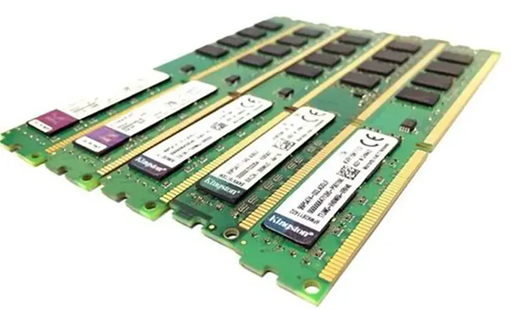
What Is DDR3 PCB?
DDR3 PCB refers to the printed circuit board used in computer systems to support DDR3 (Double Data Rate 3) memory modules. PCB stands for Printed Circuit Board, which is a flat board made of non-conductive material, usually fiberglass, with a layer of conductive pathways etched onto its surface.
The DDR3 PCB is designed specifically to accommodate DDR3 memory modules and provide the necessary electrical connections between the memory chips and the rest of the computer system. It serves as a physical platform for the memory modules to be installed and connected to the motherboard.
DDR3 is a type of computer memory that was widely used in the past but has been largely replaced by newer and faster memory technologies such as DDR4 and DDR5. However, DDR3 is still found in older computer systems and is compatible with corresponding DDR3 PCBs.
The DDR3 PCB is configured with specific layout and traces to support the electrical signaling requirements of DDR3 memory, including the necessary power delivery, data transfer rates, and signal integrity considerations. These PCBs may have multiple layers to accommodate the complex electrical pathways required for DDR3 memory operation.
It’s worth noting that the PCB itself does not determine the performance or speed of the DDR3 memory. The speed and capabilities of DDR3 memory are determined by the memory chips themselves, while the PCB provides the physical platform for their integration into the computer system.
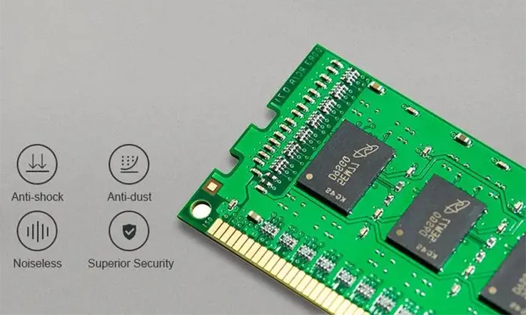
Features Of A DDR3 PCB
DDR3 PCBs possess several key features that are designed to support the specific requirements of DDR3 memory modules. Here are some of the notable features:
Memory Module Slots: DDR3 PCBs typically have multiple slots or sockets to accommodate DDR3 memory modules. These slots are designed to align with the notches on the memory modules for proper insertion and connection.
Electrical Traces: DDR3 PCBs contain intricate patterns of electrical traces that establish the connections between the memory chips on the modules and other components on the motherboard. These traces ensure proper data and power transmission between the memory modules and the system.
Signal Integrity Considerations: DDR3 memory operates at high frequencies, and signal integrity is crucial for reliable data transfer. DDR3 PCBs are designed with careful consideration for signal integrity, including controlled impedance traces, optimized routing, and ground plane placements to minimize signal noise and interference.
Power Delivery: DDR3 memory requires a stable and sufficient power supply. DDR3 PCBs incorporate dedicated power planes and capacitor arrangements to deliver clean and stable power to the memory modules, minimizing voltage fluctuations and ensuring consistent performance.
Layer Configuration: DDR3 PCBs often have multiple layers to accommodate the complex routing required for high-speed memory signaling. The number of layers may vary depending on the specific design requirements and the complexity of the system.
Decoupling Capacitors: To further enhance power stability and minimize noise, DDR3 PCBs incorporate decoupling capacitors near the memory module slots. These capacitors help reduce voltage ripples and provide localized power buffering for improved reliability.
Thermal Management: DDR3 memory modules can generate heat during operation. DDR3 PCBs may include heat sinks or thermal vias to dissipate heat and maintain optimal operating temperatures, ensuring the longevity and performance of the memory modules.
Compatibility: DDR3 PCBs are designed to be compatible with DDR3 memory modules, offering the necessary physical and electrical interfaces to ensure proper functioning and compatibility with the system’s motherboard.
It’s important to note that DDR3 PCB features can vary depending on the specific manufacturer, design choices, and intended application.
The Critical Role of PCB Layout in DDR 3 Memory Module Design
The design and production of DDR3 memory modules hinge significantly on the intricacies of DDR3 Printed Circuit Board (PCB) layout. This layout, which involves the strategic organization and interconnection of traces, vias, and components on the PCB, can drastically affect the performance and reliability of the memory module.
Signal integrity stands as one of the primary factors in DDR3 PCB layout. It necessitates a meticulous approach to the positioning and routing of traces, supplemented by appropriate termination and decoupling methodologies. The aim here is to ensure that signals maintain their integrity during transmission, with minimal distortion and interference.
Moreover, power integrity is another critical aspect to consider. This relates to the consistency and stability of the power supply directed to the memory module. It is essential to safeguard the power supply against noise, voltage fluctuations, and other potential disruptions to sustain optimal operation.
Basic Principles
DDR3 Memory Basics
Double data rate type three (DDR3) memory modules are a prevalent form of synchronous dynamic random access memory (SDRAM) found in contemporary computer systems. Compared to its predecessor DDR2, DDR3 provides higher bandwidth and reduced power consumption. The DDR interface transfers data on both the rising and falling edges of the clock signal.
Several key specifications of DDR3 modules must be contemplated when designing the printed circuit board (PCB) layout, including clock frequency, data rate, number of ranks, quantity of banks, and module density. It is imperative that the selected memory modules possess compatibility with the motherboard and processor in the system.
PCB Layout Guideline
The PCB layout for DDR3 memory necessitates meticulous design to ensure reliable performance. Numerous important guidelines should be implemented when formulating the layout:
●Minimize clock and address line lengths to reduce signal skew.
●Group data lines in sets of four or eight for proper termination and impedance matching.
●Construct power and ground planes to furnish a low-impedance path for high-speed signals.
●Control impedance of signal traces to minimize reflections and signal loss.
●Position memory modules in proximity to the processor to reduce signal delay.
Additionally, the specific recommendations of the memory module manufacturer should be followed, and a high-quality PCB fabrication process utilized. Adherence to these guidelines enables the creation of a reliable, high-performance PCB layout for DDR3 memory.
Design Considerations of DDR3 PCB
Effective PCB layout is critical for proper DDR3 operation. Key considerations include:
● Maintaining signal integrity through the use of controlled impedance traces, avoiding sharp corners, and minimizing via lengths. Proper trace terminations and matched differential pairs also help reduce signal noise and crosstalk.
● Implementing a well-designed power delivery network utilizing multiple power and ground planes to deliver clean, ripple-free power to DDR3 chips. Any gaps or voids in power/ground planes can lead to unwanted noise.
● Routing clock signals with care taken to minimize skew and match trace lengths. A dedicated clock plane helps maintain signal integrity.
● Matching trace lengths precisely, especially for address/data lines. Serpentine trace patterns can help achieve proper length matching and avoid sampling errors.
● Thoughtful component placement, orienting memory ICs to limit noise/interference. Placing memory chips close to the controller is ideal for minimizing signal loss.
In summary, seasoned designers pay close attention to signal integrity, power delivery, clock routing, trace length matching and component placement when laying out PCBs for DDR3 systems. Following best practices in these areas helps ensure reliable, optimized operation.
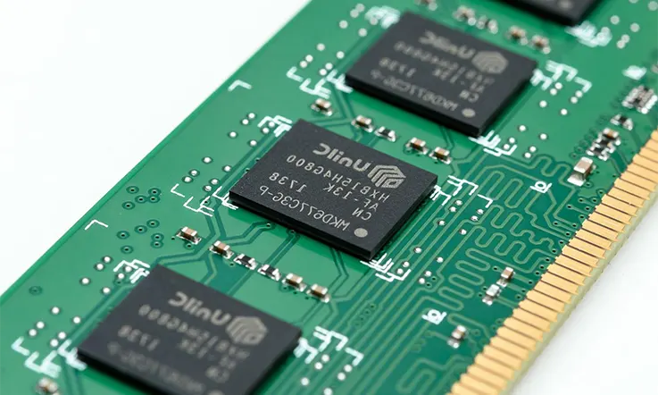
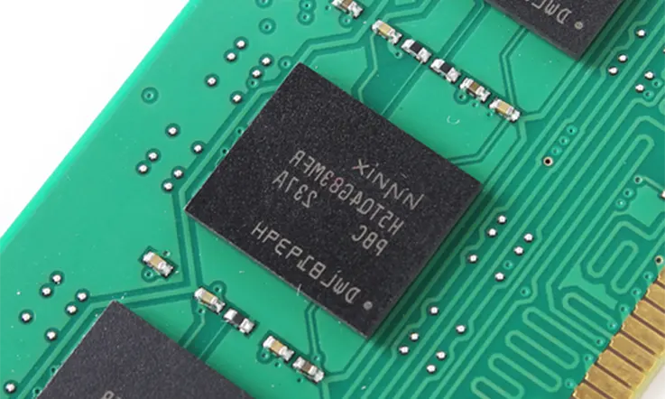
Key Components and Structure of a DDR3 PCB
Layers – Most DDR3 PCBs are multilayer, usually 4 to 8 layers, which allows tracing signals on inner layers. This isolates noise and maintains signal integrity at high speeds.
Traces – Carefully routed copper traces connect the DRAM slots to the memory controller and other system components. Trace geometry is tuned for impedance matching and noise reduction.
DRAM Slots – The PCB will have one or more DDR3 module slots. Extra slots allow installing more memory sticks for increased capacity.
Passive Components – Termination resistors, capacitors, and inductors are strategically placed to improve signaling, filter noise, and provide power buffering.
Power/Ground Planes – Entire copper layers are dedicated as power and ground planes for delivering clean, steady power to the DRAM chips. This prevents voltage drops.
Vias – Plated through-hole vias connect traces between different PCB layers. These should be minimized on critical signal paths.
Test Points – PCBs include test points or vias for probing signals during debugging and compliance testing.
Solder Mask – The solder mask insulates copper traces and prevents solder bridging between joints. It is strategically omitted from component pads.
Silkscreen – Printed markings identify components, slots, and test points. The legend helps with debugging and assembly.
How Many Types Surface Finishes For The DDR 3 PCB?
HASL (Hot Air Solder Leveling) – The most common and economical finish, applying a thin coat of solder to protect copper traces from oxidation and improve solderability.
Immersion Silver – Coats the PCB with a thin layer of silver, providing excellent solderability while preventing oxidation at high temperatures.
Immersion Tin – An alternative to silver that is deposited evenly across the board’s exposed copper. Prevents oxidation and whiskering.
ENIG (Electroless Nickel Immersion Gold) – Deposits nickel then gold layer, which protects against corrosion and provides robust connectivity even after repeated mating cycles.
ENEPIG (Electroless Nickel Electroless Palladium Immersion Gold) – Improves on ENIG performance with an extra palladium layer for bonding gold. Provides the most reliable and durable solder joints.
OSP (Organic Solderability Preservative) – Applies a temporary organic coating to PCBs, protecting copper traces until soldering when it gets displaced. A cost-effective solderability treatment.
The most optimal finish depends on budget, environmental conditions, assembly process, and performance requirements. For high-speed DDR3 PCBs, ENIG or ENEPIG provides the most robust connectivity while HASL is suitable for cost-sensitive applications. The surface finish should be specified when ordering fabricated PCBs.
What Capacities Can A DDR 3 PCB Support?
Here are the common memory capacities that a DDR3 PCB can support:
1GB – DDR3 PCBs are available with 1GB per module, providing basic memory capacity for lighter workloads.
2GB – Many mainstream PCBs support up to 2GB per module for improved multitasking and moderate application demands.
4GB – PCBs that can handle higher densities typically support up to 4GB per module. This offers ample capacity for most general computing needs.
8GB – High performance PCBs are capable of supporting memory modules up to 8GB per stick. This is ideal for intensive gaming, media editing and other memory-hungry applications.
16GB – On the higher end, advanced DDR3 PCBs can work with extremely dense 16GB modules. This provides vast memory space for complex professional and industrial applications.
32GB – Cutting edge DDR3 server PCBs support modules up to 32GB per stick, for massive total memory in high end systems. This capacity is overkill for typical consumer computing.
What Are The Considerations In Selecting A DDR3 PCB?
When selecting a DDR3 printed circuit board (PCB) for your application, there are several key factors to consider:
Interface Compatibility
Ensure the DDR3 PCB is compatible with the interface and socket on your target system’s motherboard. Using an incompatible PCB will prevent proper electrical connectivity.
Capacity Requirements
Determine the necessary capacity based on your application’s memory demands. Light productivity apps may only require low density DDR3 modules, while advanced gaming and media editing will benefit from higher density sticks.
Timing Performance
Pay attention to timing metrics like latency and clock speed. Lower latency DDR3 PCBs can improve response times during read operations. Also match the PCB’s frequency to your system board for stability. Excessively high or low frequencies can degrade performance.
Overall Compatibility
Beyond electrical compatibility, confirm the PCB matches the required form factor and specifications for flawless operation in your device. An incompatible PCB risks unreliable performance.
For assistance selecting optimized DDR3 PCBs for your application, please contact our engineering team. We can ensure you choose compatible PCBs that maximize system memory performance.