As the basic hardware for the majority of the electronics we use on a daily basis, printed circuit boards merge all the passive components and integrated circuits to create complex circuitry. This page discusses the primary distinctions between PCBA and PCB.
What is the PCB?
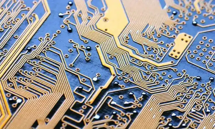
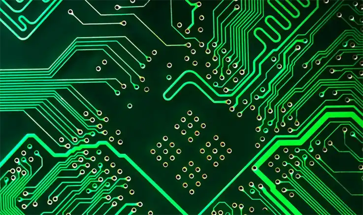
PCB is an abbreviation for “printed circuit board,” and it refers to three different things: an essential electronic component, a support for other electronic components, and a carrier for the electrical connection of other electronic components. Because it is produced by the process of electronic printing, this type of circuit board is referred to as a “printing” circuit board. PCBs are printed circuit boards, and China is home to thousands of firms that offer a variety of services related to PCB fabrication. Some companies specialize in metal core PCBs, while others concentrate on more complicated PCBs, such as hdi PCBs or 10 layer PCBs, as well as bare led printed circuit boards.
Materials used in PCBs
PCBs can be fabricated from a wide variety of substrates and materials; the choice of substrate is determined by the application criteria and the operating conditions. When designing a printed circuit board (PCB), engineers select the material based on a number of criteria, including the dielectric constant, flame retardance, loss factors for high-speed applications, mechanical strength, and thermal performance. Insulating laminate makes up the core substrate of a printed circuit board (PCB), which is known as the middle layer. The term “prepreg” refers to the insulating material that is sandwiched between two successive conducting layers.
The following materials are utilized in PCB production:
Prepreg
After being processed by specialized machines known as prepreg treaters, a glass fabric is given a resin coating before being allowed to dry. These typically consist of FR4 epoxy resin, polyimide, Teflon, and a few other materials. The resin is kept in place thanks to the glass’s role as a mechanical substrate. This particular resin begins to melt when it is subjected to high temperatures, and once all of the resin in the prepreg has melted, the material hits a thermosetting point, at which time it re-hardens and becomes exceedingly rigid. A variety of products, including airplanes and boats, make use of prepreg during the production process.
Laminates
Prepreg laminates, which are also commonly known as copper-clad laminates, are made up of sheets of prepreg that are laminated together using heat and pressure. They also have sheets of copper foil on both sides, and once the resin has hardened, the PCB laminates are similar to a plastic composite with sheets of copper foil because they both have copper foil sheets on both sides.
Solder mask
In electronic circuitry, a solder mask is an insulating layer that is typically green in color (although the color can be changed to suit the specifications of the individual customer). It is layered on top of the traces to protect the copper traces underneath from becoming oxidized when they are exposed to moisture. They also prevent the tracks from being shorted out if any conducting material is placed on a live printed circuit board. Solder masks not only extend the life of a printed circuit board (PCB), but they also leave space for the silkscreen to be applied.
Silkscreen
A silkscreen is a layer of ink trace that is used to name components and mark the boundary between those components. They help make printed circuit boards more readable and are useful in troubleshooting. They also assist in personalizing a printed circuit board (PCB) by adding company logos and names.
What are the Different Types PCB?
Single-Layer PCB
Single-sided printed circuit boards, also known as single-sided PCBs, are the most common and basic type of PCB, and they are used in the majority of electronic products.
The single-layer printed circuit board (PCB) has one coat of copper, which serves as the conducting material; a layer of solder mask, which prevents the PCB from oxidizing; and a silkscreen, which labels the components that are on the PCB.
This printed circuit board is utilized in manufacturing that is both large-scale and cost-effective.
Double Layer PCB
These printed circuit boards (PCBs) are distinguished from their one-sided counterparts by the presence of a copper layer on both sides of the board, hence the alternative name “double-sided PCBs.”
The benefit of using copper as a conducting layer on both sides is that it enables smaller PCBs.
These printed circuit boards are used in a variety of electronic devices, including phones and power converters.
Multi-Layer PCB
These printed circuit boards (PCBs) have more than two layers of the conductive material copper.
In most cases, they are manufactured by adhering together two layers of double-sided printed circuit boards (PCBs) using an insulating adhesive that is resistant to heat. These PCBs find their way into intricate technological devices.
Higher component density and greater design complexity are both made possible by multi-layer printed circuit boards.
Applications for PCBs
PCB is utilized in virtually all electrical devices, from mobile phones to LED lamps and everything in between. Every single electrical product on the market today has a PCB at its core. The use of printed circuit boards (PCBs) is growing as electronics and their applications spread throughout practically every sector of the economy. Nearly every sector is searching for ways to automate their processes with the help of more sophisticated technology, which has led to an increase in the usage of electronics.
In the realm of healthcare, numerous electronic scanners, monitoring, and measuring devices are utilized in order to keep track of the many health parameters of patients. It is necessary for these machines to operate with the highest possible degree of precision and accuracy. As a result, high-density interconnect PCBs, sometimes known as HDI boards, have been purpose-built specifically for this use. In some applications, the movement of pieces is required to be frequent; hence, flexible laminates are utilized for the same purpose.
PCB is used as the substrate in a wide variety of consumer electronics, including smartphones, household appliances, and entertainment systems. These printed circuit boards (PCBs) are manufactured at a low cost and great volume due to the use of mass production, which also ensures that quality and safety standards are met. Laminates of the FR4 epoxy type are frequently utilized in various consumer electronics applications. Machines, power converters, and devices for measuring power are all intended for PCBs that are able to withstand extreme heat, moisture, and chemicals when used in industrial applications. In most cases, polyimide laminate with copper that is twice as thick is employed for these sorts of applications.
What is the PCBA?
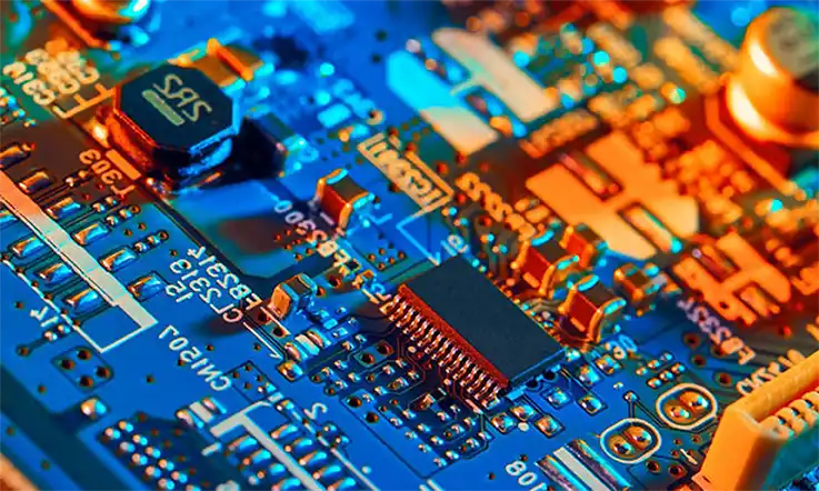
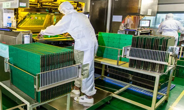
Assembly of PCBs is referred to as PCBA. A method known as surface encapsulation is used in order to complete the assembly of a variety of electronic components on the circuit board. After that comes the box assembly, which is when the printed circuit board (PCB) and the outer case are put together to make the final product. In other words, the PCB bare board goes through the SMT top part and then goes through the whole process of the DIP plug-in, which is referred to as the PCBA.
This is a method that is generally used in the country, and the usual form of writing in Europe and America is PCB’A, which adds a slant point to the beginning of each letter. PCB Assembly refers to the bare board that already has the assembly attached to it. When developing new electrical designs, engineers typically start with a prototype printed circuit board assembly (Sample PCBA) before moving on to full-scale production. after that, make a few updates and, if the market is successful, move on to mass production.
How Many types PCB Assembly Method?
The sourcing of electronic components is an important part of the PCBA manufacturing process before mounting them. These components are chosen during the PCB design phase based on the application requirements. Resistors, capacitors, integrated circuits, and microprocessor chips are classified into two types based on their mounting: surface mounted and through-hole mounted.
Surface-Mount Technology
Surface-mount technology, often known as SMT, refers to an assembly method that attaches electronic components to the top layer of a printed circuit board (PCB). It has a high degree of automation and flexibility, and it enables a larger connection density than other systems. It gives manufacturers the ability to pack intricate circuitry into relatively small components.
PCBA SMT has 4 Main Steps:
Preparing the PCB: First, the assembler applies solder paste to the areas of the board where it is required.
Placing the components: The next step is for the assembler to install the components on the board, usually with the aid of a pick-and-place machine.
Reflow soldering: After that, the boards are heated in a reflow oven by the assembler until the solder paste reaches the temperature necessary for the formation of solder joints.
Inspection: The assembler is responsible for performing inspections at multiple points throughout the SMT process. These inspections take place before component attachment, as well as before and after reflow soldering.
2. Thru-Hole Technology
In the assembly process known as thru-hole technology, holes are drilled into a printed circuit board (PCB), and it is through these holes that leads, which are electronic components, are attached. It is an older technique than SMT, but it creates a stronger connection between the board and the components, which in turn makes for more durable and reliable assemblies.
The assembly process for through-hole components can be either entirely or partially automated. The following are the stages that comprise the PCBA thru-hole process:
Drilling the holes: Drilling holes into the circuit board is the first stage in the process of installing thru-holes. These holes have to have a specific size in order to accommodate the component leads.
Placing the leads: After that, the assembler will insert the leads into the appropriate holes.
Soldering: The soldering stage is the next one to be completed in the process. This step ensures that the components are secured in their proper positions.
Inspection: Several checks are performed all the way through the process to make sure that the printed circuit board assembly will work as intended.
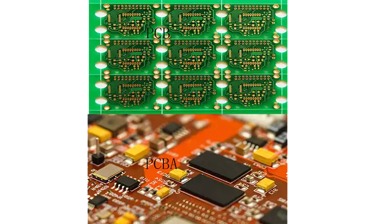
What is Different About PCB and PCBA?
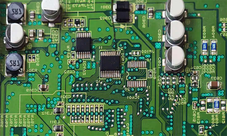
While the term “PCB” refers to the bare circuit board, “PCBA” refers to the circuit board plug-in assembly that is performed using the SMT process. The first one is a completed board, whereas the second one is just a bare boards.
PCB stands for Printed Circuit Board. It is made of epoxy glass resin and is divided into four, six, or eight layers depending on the number of signal layers. The most common layers are 4 and 6. Chips are attached to the bare board.
A printed circuit board assembly, or PCBA, is sometimes referred to as a finished circuit board; however, a PCBA can only be manufactured if all of the processes on the circuit board have been completed.
Printed Circuit Board +Assembly: PCBA
In other words, the PCBA process involves the bare circuit board going through the SMT patch and then the full process of the DIP plug-in.
PCB stands for printed circuit board. A printed circuit is, in most cases, referred to as a conductive pattern that is generated on top of a conductive material in accordance with a preset design in order to create either a printed circuit, a printed component, or a combination of the two. A printed circuit is a pattern of conductors printed on an insulating substrate that creates an electrical connection between the components of the circuit.
Therefore, the completed board of printed circuit or printed circuit is referred to as a printed circuit board, which is also referred to as printed board or bare printed circuit board.
Standard printed circuit boards (PCB) do not contain any components on the top and are more commonly known as “Printed Wiring Boards” (PWB).
JarnisTech is a PCB manufacturing and assembly factory in China. In order to offer the electronic industry a fast turnaround time and a high level of quality control, we produces both bare led printed circuit boards and PCB assemblies on the same premises.
PCB&PCBA: How to Choose a Good Printed Circuit Boards Manufacturer
You must pay special attention to a few aspects when outsourcing the customized PCB prototype to create the PCBA.
● Printed circuit board production should be the sole focus of the PCB company, not just being a simple broker.
● Maybe some manufacturers that will put a cap on your order. It is known as the Minimum Order Limit (MOL). A reputable producer of circuit boards would never place limits on the quantity of printed boards that you can purchase from them. You should be able to place an order of any quantity, from the bare minimum to the maximum.
● In order to manufacture PCBAs, the manufacturer needs to be familiar with a variety of PCB soldering procedures. It encompasses surface-mount technology, through-hole soldering, and manual soldering.
●Another important factor to consider is the lead time. You must ensure that PCBAs are delivered on time. Furthermore, the delivery must include DFM information (Design for Manufacturability). The DFM is required because your desired device cannot be manufactured without it.
● The cost of the PCBA has to be reasonable and negotiable in order to remain competitive. You should be able to negotiate the price with the manufacturer in order to receive the best prices.
Are you looking for a PCBA provider who can meet all of these needs and wondering where to find one? The good news is that JarnisTech is here to fulfill your requirements. Our skilled technical staff and the working team are responsible for preparing a variety of printed circuit boards (PCBs) and assembling them with electronic components.
In addition, We also offer competitive prices and have no minimum order requirements. You can get a completely constructed PCB in quantities ranging from one piece to one hundred thousand pieces. And finally, but by no means least JarnisTech assures that your orders will be delivered on time and that the quality of every component will be tested and certified.
Our PCB and PCBA Services
PCB production and assembly is one of JarnisTech’s specialties. We offer a wide range of options, from completely automated processes to accurate hand assembly, SMT and thru-hole technology, and board-level to full-box build assembly.
When you partner with JarnisTech, you can get our years of industry experience, prompt service, and superior products at your disposal. You can get in touch with us online, give us a call at 0086-755-23034656, or submit a quote request here to get more information about how our PCB fabrication and assembly services can assist you in achieving your printed circuit boards project.