
Designing a high-current PCB is like walking a tightrope—get it right, and you have a robust system that can handle the toughest of loads. Mess it up, and your circuits might be on their way to a meltdown (literally). Whether you’re a seasoned PCB designer or someone just stepping into this electrifying world, mastering high-current PCB design is an art and science you’ve got to get a grip on. In this guide, we’ll break down what goes into designing PCBs that can handle high currents, ensuring that your circuits perform like a well-oiled machine while maintaining rock-solid reliability.
What Exactly is a High-Current PCB?
Defining High-Current PCBs and Their Applications
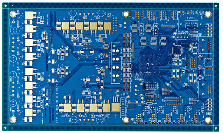
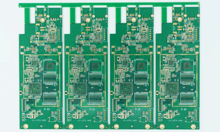
High-current PCBs are printed circuit boards that are designed to handle significantly more current than typical PCBs. You’ll find them powering up heavy-duty industrial equipment, automotive electronics, and high-power consumer devices. These boards need to be sturdy, resilient, and able to handle high current without breaking a sweat.
The main applications of high-current PCBs are:
●Industrial machinery that runs on powerful motors.
●Automotive systems, including electric vehicles and engine control units (ECUs).
●Consumer electronics that require rapid charging and discharging, like power banks and fast chargers.
●Renewable energy systems, such as solar panels and wind turbines, that demand efficient power transfer.
Common Challenges in High-Current PCB Design
Now, designing a high-current PCB isn’t all sunshine and rainbows. There are challenges galore, from managing excessive heat to ensuring that the board can handle peak loads without damaging components. If you don’t pay close attention to things like copper thickness, track width, and thermal management, your PCB could be on a fast track to failure. It’s also worth mentioning that high-current circuits can create noise, leading to electromagnetic interference (EMI) issues that wreak havoc on your system’s overall performance.
Key Factors in High-Current PCB Design
Choosing the Right Copper Thickness
One common approach to high-current design is increasing the copper thickness. A 2 oz or 3 oz copper layer is typical in high-current PCBs, but even thicker copper may be needed for extreme cases, such as power supplies or energy infrastructure systems. While thicker copper lowers the trace resistance, it also increases the board’s weight and complexity, which may affect manufacturability.
For instance, take a look at this example of a table outlining copper thickness vs. current capacity:
| Copper Thickness (oz/ft²) | Current Capacity (Amps) | Recommended Trace Width (mm) |
| 1 oz | 30 A | 1.5 mm |
| 2 oz | 55 A | 2.8 mm |
| 3 oz | 80 A | 4.2 mm |
| 4 oz | 105 A | 5.6 mm |
This table shows how increasing the copper thickness allows the board to handle higher currents without overheating, which is super useful when you’re designing high-power applications.
Key Tip: You don’t want to overdo it. Thicker copper makes the board heavier and can lead to increased costs and production challenges. Your goal is to find the optimal balance of current-carrying capacity while keeping the PCB cost-effective.
Calculating Current Carrying Capacity and Optimizing Trace Width
When it comes to handling high currents, one size does not fit all. You’ve got to calculate the current carrying capacity of your traces, which is largely determined by their width and copper thickness. Wider traces can carry more current, but you’ll need to factor in the space constraints of your PCB design.
In the words of a seasoned PCB designer, “The more current you push through a trace, the hotter it’s going to get, so you’ve got to be careful not to turn your PCB into a space heater.” By optimizing trace width and copper weight, you can ensure that your board operates efficiently without creating hot spots.
Power Distribution and Thermal Management
Optimizing Power Distribution through Layer Stackup
A well-designed layer stackup is your best friend when it comes to power distribution in high-current PCBs. By strategically placing power and ground planes, you can minimize resistance and inductance, ensuring that power is evenly distributed across the board. Multi-layer PCBs are often the go-to choice here, as they provide the flexibility needed to route power through multiple layers while keeping the board’s size manageable.
Effective Heat Dissipation Techniques
Heat is the enemy of high-current circuits, and if you don’t manage it well, you’re in for a world of hurt. Thermal vias, heat sinks, and copper pours are all effective methods for dissipating heat and keeping your components cool. Using thermal vias—holes filled with conductive material—can help transfer heat from the top layer of the PCB to the bottom, preventing hot spots and improving overall thermal performance.
The Impact of Material Selection on Reliability
High-current PCB design is not just about copper and traces. The materials you choose for your board—especially the substrate—play a big role in determining how reliable your PCB will be over time. FR4 is the industry standard for most PCBs, but when dealing with high currents and high temperatures, you might want to consider materials with better thermal conductivity and higher glass transition temperatures (Tg).
If your board will be subjected to harsh environments—think automotive or industrial applications—then choosing the right materials becomes a game of survival. You want a PCB that’ll keep on truckin’ without breaking down under the pressure.
How Optimizing Your High-Current PCB Design?
Optimizing High-Current PCB Design with Simulation Tools
No high-current PCB design is complete without thorough simulation. Using tools like Altium Designer, Cadence Allegro, or KiCad, you can model your entire board and test it under simulated current loads. These programs can predict how your PCB will behave under different thermal conditions and help you fine-tune your design for maximum efficiency.
One of the biggest advantages of simulation tools is their ability to simulate heat dissipation and current flow in real-time. By creating a thermal model of your PCB, you can visualize how heat will spread across the board and identify areas where more cooling or thicker copper might be needed.
Harnessing Simulation Tools for Better Thermal Management
When designing high-current PCBs, simulation tools are your best friend. They allow you to test various design configurations, analyze heat flow, and optimize trace width and copper thickness before ever building a physical prototype. This not only saves time but can also prevent costly mistakes.
Analyzing Heat Distribution and Power Flow
With simulation software, you can dive deep into how heat is distributed across your PCB. By identifying hot spots and areas of high current density, you can make informed decisions on where to place heat sinks, thermal vias, and copper pours to manage heat more effectively.
Improving Signal Integrity with Advanced Design Tools
High-current circuits are notorious for introducing noise into nearby signal lines. Fortunately, advanced EDA PCB design software offers tools to simulate and optimize signal integrity, reducing the risk of interference and ensuring that your board operates smoothly.
Common Pitfalls in High-Current PCB Design (and How to Avoid Them)
1)Undersized Traces: One of the biggest mistakes you can make is underestimating the trace width needed to handle high currents. Always calculate the required width based on the current your board will be handling.
2)Poor Thermal Management: Skimping on heat dissipation methods is another common pitfall. Be sure to incorporate thermal vias, heat sinks, and copper fills to keep your PCB cool under pressure.
3)Ignoring EMI and Noise: High-current circuits are noisy, and ignoring EMI shielding or signal routing can lead to major performance issues. Always design with electromagnetic compatibility in mind.
Which Thermal Management Techniques for High-Current PCBs?
Using Thermal Vias and Buried/Blind Vias for Better Heat Transfer
One of the best tricks in the book for managing heat in a high-current PCB is the use of thermal vias. These are small holes drilled into the PCB and filled with conductive material like copper to transfer heat from one layer of the board to another. Blind and buried vias, on the other hand, allow you to connect different layers without going all the way through the board, which can also help with thermal management.
Increasing Heat Dissipation with Copper Plating and Fill
When your PCB is running at high currents, even the copper traces can get hot. One way to mitigate this is by increasing the thickness of the copper plating or using copper fills to increase the amount of conductive material. This can help to spread the heat more evenly and prevent any one area from getting too hot. It’s like putting more water in the pot to keep it from boiling over.
Maximizing Efficiency with Copper Foils and Layer Thickness
Another effective technique is increasing the thickness of copper foils or adding additional copper layers to your PCB. This doesn’t just improve heat dissipation, but it also makes your board more resilient to wear and tear over time. When your copper layers are thick enough, they act like heat highways, whisking thermal energy away from sensitive components.
How Improved Reliability Enhancements for High-Current PCBs?
Optimizing Multilayer PCB Design and Trace Layout
Multilayer PCBs are like the skyscrapers of circuit board design—they allow you to fit a lot into a small footprint. By carefully stacking multiple layers, you can separate power and signal paths, minimizing interference and improving reliability. Proper trace layout is key to reducing noise and ensuring signal integrity, especially when dealing with high current and high-speed signals.
Power Distribution Network (PDN) Optimization
A robust power distribution network (PDN) is critical in high-current PCB design. It ensures that power is delivered consistently across all components without voltage drops or interference. By using a combination of wide power traces, solid ground planes, and capacitors, you can stabilize the power supply and improve the performance of the entire system.
Boosting Thermal Stability and Electromagnetic Compatibility (EMC)
High-current PCBs are prone to electromagnetic interference (EMI), which can cause all sorts of issues if not properly managed. Designing for electromagnetic compatibility (EMC) involves using shielding techniques, such as ground planes, and placing sensitive components far away from high-current traces. Additionally, ensuring thermal stability through proper material selection and heat dissipation techniques will keep your board running smoothly.
Failure Prevention Techniques in High-Current PCBs
When you’re designing high-current PCBs, you don’t just want them to work—you want them to last. These boards are running the big leagues, carrying substantial loads, and if they go down, you’re looking at costly downtime or worse. So, how do you make sure your high-current PCB can stand the test of time? Let’s dive into some failure prevention techniques that help ensure your design holds up under pressure.
Stress Testing: Pushing Your PCB to the Limit
You know that old saying, “what doesn’t kill you makes you stronger”? Well, it definitely applies to stress testing your PCB. This process is all about pushing your board to its limits, simulating conditions far harsher than anything it’ll face in regular operation. Stress testing can expose weaknesses in the design, like where a copper trace might be prone to failure or where the board gets a little too toasty under load.
Typically, engineers will run current overload tests, ramping up the current beyond normal operating conditions to see how the board handles it. If you can spot the weak points before the board hits the market, you’ll save yourself from a lot of headaches down the road. Trust me, a little extra time on stress testing pays off big time when your board handles real-world conditions like a champ.
Accelerated Thermal Cycling: Aging Your PCB Like Fine Wine
If stress testing is about finding immediate weak points, accelerated thermal cycling is like fast-forwarding time to see how your PCB will perform after years of use. By rapidly cycling between extreme hot and cold temperatures, you can simulate the long-term wear and tear your board will experience over its lifespan.
This process is especially handy for high-current boards that deal with a lot of heat. The more the current flows, the hotter the board gets, and over time, that constant heating and cooling can wear down components. With thermal cycling, you’re aging your PCB in fast forward, making sure it can handle years of punishment without breaking down.
In a nutshell, think of it like sending your board to boot camp—it’ll come out the other side ready for anything. This method gives engineers confidence that the board will keep performing long after it’s been installed, whether it’s in an EV charging station or a high-power industrial machine.
Finite Element Analysis (FEA): Crunching the Numbers
Ever wish you could peek inside your PCB to see where the real stress points are hiding? Well, with finite element analysis (FEA), that’s pretty much what you’re doing. FEA is a simulation tool that allows engineers to analyze the physical behavior of their PCB under various conditions, like heat, mechanical stress, or high current loads.
Using computer models, you can predict how the board will respond before you even manufacture it. Whether it’s looking at how heat will spread across the board or how the copper traces will handle a surge of current, FEA gives you a sneak peek into the future. It’s like having x-ray vision for your PCB.
For high-current boards, FEA can be a game-changer. You can optimize the design to avoid potential failure points, ensuring the board not only meets but exceeds your reliability standards. Plus, it’s way cheaper to make adjustments during the design phase than it is to fix issues after production. In other words, FEA is the ace up your sleeve when it comes to designing bulletproof high-current PCBs.
Burn-In Testing: The Last Line of Defense
Once you’ve put your design through stress testing, thermal cycling, and FEA, there’s still one last trick in the book: burn-in testing. This technique involves running the PCB at its maximum rated current and temperature for an extended period. Think of it as a final “dress rehearsal” before the board goes into the field.
By running the board under maxed-out conditions, you’re looking to catch any last-minute issues that could cause problems down the road. Components that might work fine at normal conditions can show signs of wear or even fail under burn-in testing. If your board can pass this, it’s ready to roll.
The whole idea behind burn-in testing is to give your board a taste of what’s coming. It’s like taking a car for a test drive in extreme conditions—if it performs well there, you know it’s good to go. Plus, any problems that arise during burn-in are usually easy to spot and fix, saving you from having to deal with faulty products down the line.
Pro Tip: Don’t just test at standard conditions—push your PCBs to their limits with extreme temperature and current load simulations. This way, you’ll know exactly how they’ll perform when the stakes are high.
Real-World Case Studies: High-Current PCBs in Action
When it comes to high-current PCB designs, nothing beats real-world examples to show how these technologies are applied across industries. From electric vehicles (EVs) to industrial power systems, high-current PCBs are the backbone of countless innovations. Let’s check out how these boards are used in some cutting-edge fields.
Electric Vehicle (EV) Charging Systems – Powering Up the Future
If there’s one industry where high-current PCBs are making waves, it’s the electric vehicle (EV) sector. Imagine this: you pull up to a charging station and plug in your EV. In that moment, your car is drawing an enormous amount of current, all managed by a high-current PCB. These boards are specially designed to handle fast charging without overheating, ensuring that your EV gets juiced up quickly and safely.
Take, for instance, the Tesla Supercharger. It relies on high-current PCBs to deliver up to 250 kW of power directly into the vehicle’s battery. The trick here isn’t just about getting the car charged fast—it’s about managing that load without frying the board. Copper traces are thickened to carry the current, while thermal management strategies like heat sinks and thermal vias are employed to keep things cool under pressure.
The real beauty? These PCBs are designed to handle massive current surges during peak charging, while maintaining their performance over repeated cycles. So, next time you charge your EV in minutes rather than hours, you can thank the high-current PCB working behind the scenes.
Industrial Power Supplies – Keeping the Heavy Machinery Rolling
In factories and large industrial settings, you can’t afford downtime. These environments need consistent, high-power delivery to keep machines humming. That’s where high-current PCBs step up to the plate. Whether it’s powering massive robotic arms or driving conveyor belts, these boards are the lifeblood of industrial power systems.
For example, automated assembly lines in car manufacturing require substantial power to drive their motors and actuators. High-current PCBs designed for these systems distribute power across different parts of the machine, ensuring that everything runs smoothly, even when the current spikes.
In one notable case, an American auto manufacturer used high-current PCBs in its robotic welding stations. The PCBs were designed with thick copper layers, wide power planes, and via stitching to carry hefty electrical loads without faltering. These robust boards allowed the machines to operate continuously without burning out, providing reliability in a high-demand, fast-paced setting.
Medical Equipment – Powering Life-Saving Technology
When it comes to medical equipment, the stakes couldn’t be higher. Devices like MRI machines, CT scanners, and heart monitors require precise and reliable high-current PCBs. These boards are responsible for powering complex systems that directly affect patient care, and they have to do so without any hiccups.
Consider an MRI machine, which generates powerful electromagnetic fields. This requires a high-current PCB capable of delivering stable, consistent power to the system’s magnets. If the PCB overheats or fails, the entire machine could shut down mid-scan—a nightmare scenario in a medical setting. To prevent this, designers use multi-layered PCBs with enhanced thermal management systems, ensuring the board can handle prolonged use without a hitch.
In one hospital, an MRI manufacturer turned to high-current PCBs with thermal vias and heavy copper plating to handle the massive energy demands. These boards are key to maintaining the reliability of the MRI systems, ensuring that patients get the scans they need when they need them.
Data Centers – Fueling the Digital Backbone
Think about this for a second: every Google search, Netflix stream, or video game session relies on massive data centers powered by high-current PCBs. Data centers are the unseen infrastructure of our digital lives, and these facilities run 24/7, requiring enormous amounts of power. High-current PCBs keep servers running by efficiently distributing electricity across thousands of racks of equipment.
In hyperscale data centers, where downtime is measured in lost millions, high-current PCBs play a pivotal role in power distribution and thermal management. These PCBs use wide power planes, thick copper layers, and specialized cooling techniques to manage the vast current loads required by modern processors and storage devices.
For example, one leading tech company installed high-current PCBs in its server farms, designed to carry 48V power through the entire facility. These boards utilized via stitching and high-conductivity copper to distribute power evenly while dissipating the heat generated by the immense current. The result? A reliable, high-efficiency setup that keeps our digital world running without a glitch.
Advanced PCB Design Techniques for High-Current Applications: Taking It to the Next Level
When you’re dealing with high-current PCBs, sometimes the basics just don’t cut it. You’ve got to dig deeper, get a little fancy with your design techniques to keep everything flowing smoothly. It’s like trying to navigate rush hour traffic—sometimes you’ve just gotta find a better route. So let’s talk about a few advanced tricks of the trade that can really help you spread the load and keep your board from getting bogged down.
Multi-Layer Boards: Spreading the Load
You might think of a multi-layer PCB as the king of efficiency when it comes to current distribution. Instead of relying on a single-layer or even a double-layer board, a multi-layer setup gives you the ability to split the current load across multiple planes. That’s right—more layers mean more room to breathe. Think of it like building a highway with multiple lanes instead of a narrow one-lane road. You’re going to handle way more traffic without any bottlenecks.
For high-current designs, you can dedicate specific layers to power and ground planes, which helps distribute the current more evenly. This not only reduces the chances of any hot spots forming on your board but also makes your entire design more efficient. And let’s not forget about how it can lower electromagnetic interference (EMI), which is something every engineer loves to avoid.
When done right, multi-layer boards can also make your life easier when it comes to thermal management. By spreading the heat across layers, you minimize the chances of frying any components. It’s like wearing a jacket in layers—you stay warm, but you don’t overheat. In the world of high-current PCBs, it’s all about keeping cool under pressure.
Pro Tip: Use wide power planes and strategically placed vias to minimize resistance and ensure even current distribution across all layers of the PCB.
Parallel Trace Routing: Sharing the Burden
Another trick for high-current PCBs is parallel trace routing. Instead of sending all your current through a single fat trace, why not split it up? It’s like carpooling—when multiple cars share the load, traffic moves a lot smoother. Same deal here. By routing parallel traces, you can spread the current across multiple pathways, reducing the overall load on any single trace.
This technique is especially useful when you’re working with larger currents, where a single trace might overheat or just be too bulky for your design. By breaking it up into smaller, parallel traces, you’re reducing resistance and helping the current flow like a river instead of a trickling stream.
But here’s the kicker: you’ve got to make sure those traces are balanced. If one trace is shorter or has less resistance than the others, it’s going to take more of the load, which defeats the whole purpose. So keep those traces equal in length and width to make sure everything runs like a well-oiled machine.
High-Current Via Stitching: The Power of Connection
Now, let’s talk about high-current via stitching. When you’re running hefty currents through a multi-layer board, you’ve got to find a way to connect those layers efficiently. That’s where via stitching comes in. You can think of vias like little tunnels connecting different floors of a skyscraper. They allow current to pass from one layer to another, and the more vias you have, the more current you can move around without causing any stress.
For high-current PCBs, it’s not enough to just use a couple of vias here and there—you need to create a whole network of them. This is where via stitching comes into play. By placing multiple vias along the current path, you ensure that the current can travel smoothly between layers without any bottlenecks.
Via stitching also helps distribute heat more evenly, which is a big plus in high-current designs. Remember, heat is the enemy when you’re pushing serious current, and vias give it an easy escape route. It’s like opening all the windows in a hot room—suddenly, everything cools down.
One thing to keep in mind: make sure your vias are properly plated and able to handle the current load. Skimping on this can lead to some serious issues down the line, and nobody wants that.
Balancing Act: Combining Techniques for Maximum Efficiency
Here’s where the magic happens—combining all these advanced techniques into one seamless design. Multi-layer boards, parallel trace routing, and via stitching all work hand-in-hand to make sure your PCB can handle high-current applications without breaking a sweat.
By using multi-layer boards, you get the benefit of distributing both current and heat across several planes. Meanwhile, parallel trace routing helps to ensure no single trace is overburdened, and via stitching keeps the current flowing smoothly between layers. The result? A rock-solid PCB that can handle the demands of industrial power systems, EV charging stations, and even medical devices.
And don’t forget, implementing these techniques also helps with long-term reliability. You’re not just building a board that works today—you’re building one that’s going to keep working for years down the road. Engineers, manufacturers, and procurement teams all appreciate a design that doesn’t require constant rework or repairs.
Future Trends in High-Current PCB Design
The field of PCB design is always evolving, and with the rise of electric vehicles, renewable energy, and high-performance computing, the demand for high-current PCBs will only grow. Here are a few trends to keep your eye on:
1)Advanced Materials: As the need for higher efficiency and durability grows, new materials like ceramic substrates and metal-core PCBs are being developed to handle extreme currents and temperatures. These materials not only enhance the current-carrying capability but also significantly improve thermal management.
2)Integration with Power Electronics: High-current PCBs will continue to see deeper integration with power electronics, especially in applications like inverters, converters, and battery management systems. This trend will push designers to create boards that can handle not only high current but also high voltage, without sacrificing safety or performance.
3)Smarter Simulation Tools: Advanced simulation software is becoming a must for high-current designs. Tools that allow you to simulate both electrical performance and thermal characteristics at the same time will be vital for ensuring your design can handle real-world conditions. This will help catch potential failures early and optimize the design for both efficiency and cost-effectiveness.
4)Miniaturization: Despite the need for handling high currents, there is a constant push to make devices smaller and more compact. This challenge drives innovation in trace routing, layer stacking, and the overall PCB architecture to fit more power into less space without compromising on performance or safety.
Final Thoughts
Take Your High-Current PCB Designs to the Next Level
Whether you’re working on electric vehicles, industrial power supplies, or the next breakthrough in telecommunications, mastering high-current PCB design is essential to the success of your project. With the right balance of copper thickness, heat management strategies, and advanced design techniques like via stitching, you can ensure that your PCBs perform reliably even under the most demanding conditions.
If you’re ready to take your high-current PCB designs to the next level, don’t hesitate to explore more advanced design resources, consult experts, or even start your own simulation with cutting-edge software. The future is electric, and high-current PCBs are powering the way forward.


