
In today’s high-performance electronics world, PCB designers and engineers face increasing challenges when it comes to heat management and material selection. High-TG (high glass transition temperature) PCBs have emerged as a critical solution for these challenges. Whether you’re working on applications in the automotive, aerospace, or consumer electronics industry, high-TG PCBs allow you to operate in extreme temperature environments while ensuring structural integrity and maintaining electrical performance.
But designing a High-TG PCB stack-up is not as straightforward as choosing any material and layering them together. Every decision—whether it’s the selection of materials, via technologies, or even the number of layers—impacts the board’s thermal performance and overall cost.
This article breaks down the key elements of High-TG PCB stack-up design, offering insights into material selection, thermal management, manufacturing best practices, and more. By the end, you’ll have a solid understanding of how to create robust, reliable PCBs for your high-temperature applications.
What is High-TG PCB Stack-Up?
Understanding High-TG PCBs
High-TG PCBs are those designed with materials that can withstand elevated temperatures without losing their mechanical integrity. The glass transition temperature (TG) is the point at which the material changes from a rigid state to a more pliable or rubbery state. For standard PCBs, this TG value usually hovers around 130°C, but in High-TG PCBs, it typically starts at 170°C and goes upward. This makes these boards better suited for high-temperature environments and more resistant to thermal stress, which can warp layers and cause failures in regular boards.
While it might sound like something straight out of a sci-fi movie, this temperature change is a very real problem in industries like automotive and aerospace, where the internal temperature of systems can easily exceed those thresholds. Think about how hot a car’s engine bay can get, and you’ll quickly understand the need for better heat-resistant materials.
Importance of PCB Stack-Up in High-TG Designs
So, why does the stack-up matter in a High-TG PCB? Well, it’s the backbone of your board’s functionality. Proper layer arrangement, material choices, and component placement are essential for ensuring the board performs well under these higher temperatures. Poorly planned stack-ups can lead to issues like signal loss, impedance mismatches, or even worse—thermal failure. In High-TG designs, you’ve got to keep in mind that each layer isn’t just a piece of material but a key part of how the whole system dissipates heat and handles signals.
Let’s break it down further: if you’re building a board for a complex system like an electric vehicle or a high-performance computer, heat management becomes a top priority. A well-designed stack-up not only prevents overheating but also improves signal integrity by carefully balancing the layers between power, ground, and signal.
Key Components of High-TG PCB Stack-Up
Material Selection for High-TG PCBs
Choosing the right materials for a High-TG PCB is like picking the right engine for a race car—you wouldn’t put a V4 in a Formula 1 car. Standard FR4 materials just won’t cut it for high-temperature or high-reliability applications. Instead, designers turn to materials like FR408, polyimide, and Rogers materials, which offer higher thermal resistance and superior electrical performance.
FR408 (High-TG FR-4 Material)
FR408 is an advanced FR-4 material that offers enhanced performance, particularly in high-temperature and high-frequency applications.
●Glass Transition Temperature (Tg): ~180°C
●Decomposition Temperature (Td): ~345°C
●Thermal Expansion (Z-axis): 2.8% at Tg
●Dielectric Constant (Dk): 3.7 at 10 GHz
●Dissipation Factor (Df): 0.010 at 10 GHz
Temperature Performance:
●Performs reliably in environments up to 170-180°C.
●Commonly used in automotive, aerospace, and high-speed digital applications.
●FR408 is great for its low dielectric constant and high signal integrity at high frequencies.
Polyimide
Polyimide materials are known for their exceptional thermal stability, making them ideal for high-temperature applications.
●Glass Transition Temperature (Tg): ~250-260°C
●Decomposition Temperature (Td): ~400-450°C
●Thermal Expansion (Z-axis): 1.2% at Tg
●Dielectric Constant (Dk): 3.4 at 10 GHz
●Dissipation Factor (Df): 0.004 at 10 GHz
Temperature Performance:
●Polyimide PCBs can handle extreme temperatures ranging from 200-260°C.
●Often used in aerospace, military, and oil drilling applications where extreme heat is a factor.
●Polyimide is often chosen for its exceptional thermal stability, making it a go-to for aerospace and military applications.
Rogers 4000 Series (Rogers 4350B)
Rogers materials are widely known for their excellent high-frequency performance and thermal stability.
●Glass Transition Temperature (Tg): 280°C
●Decomposition Temperature (Td): ~390°C
●Thermal Expansion (Z-axis): 1.8% at Tg
●Dielectric Constant (Dk): 3.48 at 10 GHz
●Dissipation Factor (Df): 0.0037 at 10 GHz
Temperature Performance:
●Operates well in environments up to 280°C.
●Ideal for high-frequency RF/microwave applications, including communication systems and radar equipment.
●Rogers materials, particularly the 4000 and 5000 series, are often used for high-frequency applications where signal loss must be minimized.
Isola FR408HR
Isola’s FR408HR is an advanced FR-4 material used in PCBs requiring high-Tg and low Dk.
●Glass Transition Temperature (Tg): ~230°C
●Decomposition Temperature (Td): ~350°C
●Thermal Expansion (Z-axis): 2.2% at Tg
●Dielectric Constant (Dk): 3.65 at 10 GHz
●Dissipation Factor (Df): 0.009 at 10 GHz
Temperature Performance:
●Performs well in environments up to 230°C, ensuring reliable thermal and mechanical performance for high-speed digital applications.
Comparison Table: Material Performance Under Temperature
| Material | Tg (°C) | Td (°C) | Dk (at 10 GHz) | Df (at 10 GHz) | Z-axis Expansion (%) | Max Temp Range (°C) |
| FR408 | 180 | 345 | 3.7 | 0.010 | 2.8% | 170-180 |
| Polyimide | 260 | 400-450 | 3.4 | 0.004 | 1.2% | 200-260 |
| Rogers 4350B | 280 | 390 | 3.48 | 0.0037 | 1.8% | 280 |
| Isola FR408HR | 230 | 350 | 3.65 | 0.009 | 2.2% | 230 |
When you’re stacking these materials, you’re essentially building the foundation of your entire design. The key here is to balance electrical performance with thermal properties, ensuring that the board can handle the electrical load without overheating.
Copper Thickness and Layer Count
Copper thickness plays a significant role in both the current-carrying capability and the thermal management of a High-TG PCB. Boards with thicker copper layers are better at dissipating heat, which is crucial for high-current applications like power converters or motor controllers. However, thicker copper also increases the cost and may affect the board’s flexibility, so there’s always a trade-off between performance and manufacturability.
As for layer count, you’ve got to consider the complexity of your design. A simple 4-layer stack-up might be enough for basic applications, but if you’re working with more advanced designs, especially ones that require signal integrity and controlled impedance (more on that later), you’ll likely need at least 6 or more layers.
●4-Layer PCB Stack-Up: This is typically used in less complex designs, where the layer configuration might look something like this: signal layer, ground plane, power plane, and another signal layer.
● 6-Layer PCB Stack-Up: Often found in more complex, high-speed designs, this configuration offers improved signal integrity by adding additional ground and power planes.
Here’s a simple illustration of a 6-layer PCB stack-up for a High-TG board:
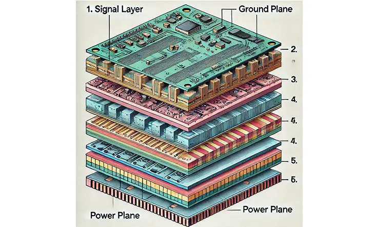
1.Signal Layer
2.Ground Plane
3.Signal Layer
4.Power Plane
5.Ground Plane
6.Signal Layer
PCB Stack-Up Design Considerations for High-TG PCBs
Signal Integrity and Controlled Impedance
In high-speed circuits, controlling impedance is everything. A mismanaged impedance can cause signal reflections, which ultimately degrade the performance of the PCB. When designing for High-TG boards, you’ll need to pay extra attention to how the stack-up affects the impedance.
For instance, one common trick designers use is to place signal layers between ground and power planes. This helps to stabilize the impedance and reduce noise—a technique especially useful in RF and microwave applications, where signal loss can be a real headache. Additionally, materials with a low dielectric constant (like Rogers 4000) can improve signal performance at high frequencies.
Thermal Management in High-TG Stack-Up Designs
We’ve been talking about heat this entire time, but let’s get specific about how to manage it in a High-TG PCB. A combination of power planes, ground planes, and thermal vias can help direct heat away from sensitive components and dissipate it across the board.
Thermal vias, in particular, are like the unsung heroes of PCB design. These small copper-filled holes help transfer heat from the top layers down to the cooler, internal layers, much like the radiator in your car engine. Without them, the heat would get trapped on the surface, eventually leading to thermal stress and failure.
Here’s a thermal management layer setup:
1.Top Layer (Signal and Components)
2.Thermal Vias to Inner Ground Plane
3.Inner Ground Plane (Heat Dissipation)
4.Inner Power Plane
5.Bottom Layer (Additional Components or Signal Routing)
Via Design and Placement
Speaking of vias, in multilayer designs, the placement of vias (especially blind and buried vias) plays a significant role in both thermal and electrical performance. Blind vias connect outer layers to inner layers without going through the entire board, while buried vias connect only inner layers, maximizing space for signal routing.
Using blind and buried vias can significantly increase the routing density of your design, allowing for more complex circuits without needing to increase the board’s size. However, there’s always a catch—adding these types of vias increases manufacturing complexity and cost.
Layering Strategy and Stack-Up Configuration
The configuration of your PCB stack-up determines its thermal, electrical, and mechanical characteristics. When designing High-TG PCBs, the following strategies are commonly employed:
Signal Layer Management
Top and Bottom Layers: Typically reserved for high-speed signals or power planes, these layers are crucial in managing heat dissipation and maintaining signal integrity.
Inner Signal Layers: Placing critical signal traces in inner layers protects them from electromagnetic interference (EMI) and thermal stress, which can degrade signal quality over time.
Power and Ground Planes
Ground planes are essential for reducing electromagnetic interference (EMI) and providing a solid reference for signal integrity. In High-TG stack-ups, power and ground planes should be carefully placed near signal layers to manage both thermal flow and signal reflection.
Dielectric Layers
The dielectric constant (Dk) of each insulating layer plays a major role in the overall signal integrity and heat management of the stack-up. High-TG materials generally have a stable Dk even at elevated temperatures, ensuring that the electrical properties of the board remain constant under thermal stress.
Advanced Techniques in High-TG PCB Stack-Up
As designs become more complex, advanced techniques such as via-in-pad technology and buried vias are gaining popularity.
Via-in-Pad Technology
Via-in-pad technology is an excellent method for reducing the distance between components, helping to enhance both signal performance and space utilization. By placing vias directly beneath components, designers can save space, enabling more compact and higher-density boards.
Buried and Blind Vias
In a multi-layer High-TG PCB, the use of buried and blind vias becomes essential. Buried vias connect inner layers, while blind vias connect the outer layer to one or more inner layers without passing through the entire board. These types of vias enhance signal routing efficiency while minimizing surface clutter and improving thermal dissipation.
Common High-TG PCB Stack-Up Configurations
4-Layer High-TG PCB Stack-Up
A 4-layer stack-up is often sufficient for simpler designs but can still offer excellent performance in high-temperature environments. Typically, the layers would be arranged with two signal layers sandwiching a power plane and a ground plane. This configuration provides enough heat dissipation for low to medium complexity applications.
6-Layer High-TG PCB Stack-Up
In more advanced designs, a 6-layer stack-up is often preferred. The additional layers help distribute power more evenly and improve signal integrity by separating the power and ground planes. This configuration is particularly useful in high-frequency applications, where controlled impedance and low signal loss are required.
Let’s take a typical 6-layer High-TG PCB stack-up as an example of a well-structured design:
●Layer 1 (Top Layer – Signal Layer): Often used for routing critical signals and high-frequency components.
●Layer 2 (Ground Plane): A dedicated ground layer to reduce EMI and improve signal integrity.
●Layer 3 (Signal Layer): For routing less critical signals, protected by adjacent ground planes.
●Layer 4 (Power Plane): Distributes power across the board, with thermal management to prevent overheating.
●Layer 5 (Ground Plane): Helps to maintain a stable reference for signals and improves heat dissipation.
●Layer 6 (Bottom Layer – Signal Layer): Typically used for lower-speed signal routing.
8-Layer High TG Stack-up
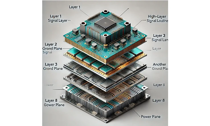
A typical 8-layer High-TG PCB stack-up, which offers more routing layers and better signal integrity for high-frequency applications.
Please find the following 8-Layer High-TG PCB Stack-Up:
Layer 1 (Top Signal Layer): Used for high-speed and critical signal routing.
Layer 2 (Ground Plane): Ground layer for EMI reduction.
Layer 3 (Inner Signal Layer): Additional signal routing.
Layer 4 (Power Plane): Power distribution and heat management.
Layer 5 (Ground Plane): Dedicated to signal integrity and thermal management.
Layer 6 (Inner Signal Layer): Used for less critical signal routing.
Layer 7 (Ground Plane): Ground plane to ensure minimal signal noise.
Layer 8 (Bottom Signal Layer): Final signal routing layer.
Advanced 10+ Layer High-TG PCB Designs
When you get into the realm of 10-layer or more, you’re looking at some serious high-performance applications like RF, microwave, and aerospace designs. The extra layers allow for more precise control over impedance and signal routing while providing better thermal management.
Applications of High-TG PCB Stack-Up
Automotive: Navigating High-TG PCB Stack-Up in Electric Vehicles
In the world of electric vehicles (EVs), the performance and durability of High-TG PCBs are vital. These stack-ups are not just dealing with regular circuits; they’re withstanding temperatures that would make other materials bend under the pressure.
Surviving the Heat of the Road
EVs, particularly their powertrain systems, battery management, and inverters, create massive amounts of heat due to high currents and power requirements. Standard PCBs just won’t do the trick here. With High-TG PCBs, the glass transition temperature is elevated, meaning these boards can handle the intense heat without warping or degrading. It’s like stepping into a sauna but keeping your cool—no matter how hot things get. For engineers working on high-voltage components, this means better stability and consistent performance over time, even when the vehicle is pushed to its limits.
Taking a Beating on the Road
Beyond heat, there’s also the challenge of constant vibration. Let’s be real—roads aren’t exactly smooth, and those bumps and jolts send shockwaves through an EV’s components. This is where High-TG PCB stack-ups shine, providing that extra durability to keep everything together, no matter how bumpy the ride. Designers can use these PCBs to create systems that stand the test of time without cracking under physical stress. For anyone building EVs, it’s about reliability in the long run.
Aerospace: High-TG PCB Stack-Ups in the Skies
The demands on PCBs in aerospace are through the roof. We’re talking avionics and satellite communications, where the stakes are sky-high, and so are the temperatures. High-TG PCB stack-ups are a game-changer here, keeping avionics systems running smoothly in the most extreme conditions.
Heat and Cold, No Problem
Up in the air, things get wild. From blazing heat near engines to the bone-chilling cold of high-altitude orbits, PCBs are subjected to all sorts of thermal challenges. High-TG PCBs don’t sweat it—they’re built to handle temperature extremes, which is essential for ensuring long-term reliability. Imagine a satellite soaring through space; the last thing you want is a board that can’t handle temperature swings. Thanks to High-TG stack-ups, signal integrity is maintained, allowing sensitive equipment to operate without a hitch, even in zero-gravity conditions.
High-Frequency Needs in Avionics
Avionics often deal with high-frequency signals over long distances, making signal integrity mission-critical. High-TG PCBs offer stack-up designs with low signal loss, ensuring communication remains clear. These boards can integrate complex RF systems into their layers, creating stable connections in dynamic aerospace environments. It’s like designing for a marathon runner—you need endurance and reliability at every step.
Consumer Electronics: High-TG PCB Stack-Ups Powering the Future
While aerospace and automotive industries demand robust solutions, High-TG PCBs aren’t just for heavy-duty tech. In fact, consumer electronics, especially high-performance devices like gaming consoles and smartphones, benefit from this advanced technology more than you might think.
Powering Next-Gen Gadgets
Ever wonder why your phone doesn’t melt during a video call or your gaming console doesn’t overheat during an intense multiplayer session? It’s because devices like these are increasingly relying on High-TG PCB stack-ups to handle the heat generated by high processing loads. Whether it’s a laptop running multiple applications or a home server crunching data, these boards ensure that internal temperatures don’t spiral out of control. They’re the unsung heroes, keeping your tech cool while you’re busy leveling up or binge-watching the latest series.
Smaller, More Powerful Designs
The demand for slimmer, more powerful devices is at an all-time high. Consumers want gadgets that pack a punch, without having to carry a brick around in their pockets. High-TG stack-ups allow manufacturers to design smaller and more compact devices by layering circuits in a way that maximizes efficiency and performance. From smartphones to smartwatches, these PCBs allow for that extra horsepower without the heat.
Manufacturing Capabilities for High-TG PCB Stack-Up
Tolerances and Manufacturing Techniques
Precision is the name of the game when it comes to manufacturing High-TG PCBs. A poorly manufactured board can lead to significant issues, such as warping or layer misalignment, particularly when you’re dealing with multiple layers and high-performance requirements. With High-TG boards, you’re often working within much tighter tolerances to ensure both the electrical and mechanical properties are maintained.
Advanced manufacturing techniques like laser drilling for vias and high-precision lamination processes are crucial. Manufacturers typically work with tolerances as tight as +/- 0.05 mm for high-reliability boards, which are common in industries like aerospace and medical devices.
●Blind vias: These connect outer layers to one or more inner layers without passing through the entire board, which helps save space and optimize signal routing.
●Buried vias: These connect only inner layers, reducing surface clutter and increasing routing density without compromising reliability.
Tolerances are especially critical in high-speed or high-frequency applications where even the smallest misalignment can throw off signal integrity. If you’re not paying close attention to the manufacturing capabilities and tolerances of your supplier, you’re just asking for trouble down the line.
Testing and Quality Assurance
Quality assurance is an absolute must in the production of High-TG PCBs, particularly given their use in critical industries like aerospace, automotive, and industrial applications. Rigorous testing is needed to ensure these boards can handle extreme environments. Key tests include thermal cycling, where the board is repeatedly heated and cooled to simulate real-world operating conditions. This helps to ensure that the board’s materials and stack-up can endure without delaminating or cracking.
Another essential test is Design for Manufacturing (DFM). This process ensures that the design can be efficiently manufactured without any errors or unnecessary complexity. You don’t want to design a board that looks great on paper but can’t be produced without skyrocketing costs or impossible tolerances.
For high-frequency boards, impedance testing and signal integrity analysis are performed to ensure that the electrical properties of the board are within the specified limits. These tests help to prevent signal loss, reflection, and other performance issues that could lead to system failure.
Best Practices for High-TG PCB Stack-Up Design
Balancing Cost and Performance
Every PCB designer knows that you can’t just throw money at a problem and expect it to be solved. High-TG PCBs are no different—there’s always a balance between cost and performance. Using exotic materials like Rogers can give you incredible signal performance, but it’ll also increase your material costs. Meanwhile, using standard FR4 materials might be cheaper, but you sacrifice temperature resistance and durability in the process.
To strike the right balance, it’s crucial to work closely with your manufacturer. They can offer insights into what materials and layer configurations will meet your performance needs without unnecessarily inflating costs. You might not need the most advanced materials for every layer, but instead, a mix of standard and high-performance materials where appropriate.
Partnering with Experienced PCB Manufacturers
Not all manufacturers are created equal. When you’re designing for High-TG applications, it’s essential to work with manufacturers that have experience producing high-reliability boards. Look for partners who have a proven track record in industries like aerospace, automotive, and telecommunications, where the demands on the board are at their highest.
Additionally, experienced manufacturers will be able to offer DFM feedback, helping you optimize your design for manufacturability without sacrificing performance. They can help you avoid common pitfalls, like over-specifying materials or underestimating the complexity of your stack-up, both of which can lead to costly delays or reworks.
Emerging Trends in High-TG PCB Stack-Up Design: 5G, IoT, and AI
As we push further into a tech-driven future, High-TG PCB stack-ups are stepping up to the plate to meet the growing demands of advanced technologies like 5G, IoT (Internet of Things), and AI electronics. These trends are reshaping industries, and the need for robust, heat-resistant PCBs has never been more pressing. Let’s dive into how each of these technologies is demanding more advanced High-TG PCB designs.
5G Technology: High-TG PCBs Keeping the Pace
The rollout of 5G networks is a game-changer for global communication. With speeds up to 100 times faster than 4G and the ability to connect more devices than ever before, 5G is pushing the boundaries of high-frequency signals and data transfer.
Why High-TG PCB Stack-Up is Essential for 5G?
In 5G technology, signal integrity is everything. With high frequencies and faster data rates, even the smallest PCB hiccup can lead to major issues like signal loss or interference. This is where High-TG PCBs come into play. The elevated glass transition temperature allows these stack-ups to maintain their form and function under intense thermal stress, ensuring that 5G base stations and communication devices perform consistently, no matter the conditions.
Heat is the Name of the Game
With the increased power density of 5G components, overheating is a big concern. Picture this: 5G infrastructure needs to run hot, but it can’t melt under the pressure. That’s where High-TG PCBs make all the difference—they can handle the heat without breaking a sweat. Whether it’s in antennas, routers, or even mobile devices, these boards keep the 5G world spinning without thermal breakdowns.
High-TG PCBs at the Heart of Connectivity
The Internet of Things (IoT) is weaving itself into nearly every aspect of life. From smart homes to industrial automation, IoT devices are generating vast amounts of data that require powerful, efficient electronics to process and relay information.
High-TG PCB Stack-Ups for Reliable IoT Devices
IoT devices are often found in extreme environments—think about a smart sensor in an outdoor pipeline or a tracking device in a high-vibration industrial setting. These environments call for High-TG PCB stack-ups to ensure longevity and performance. The ability to withstand higher temperatures means that IoT devices can run for longer without failure, making them more reliable in harsh conditions.
Miniaturization Meets Performance
One of the biggest trends in IoT is the push for miniaturization—packing more functionality into smaller devices. But miniaturization creates more heat in a confined space. High-TG PCBs allow IoT designers to achieve this without sacrificing reliability, as the material’s stability at elevated temperatures prevents warping or delamination in miniature, compact devices. This makes IoT devices like smart wearables, sensors, and smart home gadgets more durable and efficient.
AI Electronics: Power-Hungry Machines Need High-TG PCBs
The AI revolution is heating up—literally. AI-powered systems like deep learning servers, data centers, and advanced robotics are all power-hungry machines that require high-performance PCBs to keep up with their processing needs. AI applications generate a ton of heat due to the sheer amount of data being crunched at lightning speeds.
High-TG PCB Stack-Up: The Backbone of AI Hardware
The higher the processing power, the more heat a device generates. AI systems need PCBs that can withstand high power without compromising performance. That’s where High-TG PCB stack-ups shine. They’re built to endure the high temperatures AI electronics experience during intensive tasks, ensuring that signal integrity and electrical performance remain stable, even when the workload gets heavy.
Enhancing Durability for the AI Era
Think about AI-driven robotics in industrial settings. They are often exposed to high temperatures, dust, and heavy vibrations. With High-TG PCBs, these machines can maintain performance without breaking down. This gives manufacturers the ability to push the boundaries of AI technology, knowing that the infrastructure beneath can handle the pressure—just like a reliable old truck on a cross-country road trip.
Best Practices for Collaborating with PCB Manufacturers
As we wrap up this deep dive into High-TG PCB stack-up design, it’s clear that the future of electronics—from 5G to AI—relies heavily on choosing the right PCB materials and design techniques. But understanding the technology is only half the battle. Collaborating with a skilled PCB manufacturer is what truly brings these designs to life.
Collaborate with Your Manufacturer Early
Here’s a tip from the trenches: the earlier you involve your PCB manufacturer in the design process, the smoother your project will go. By aligning on material selection, stack-up configuration, and manufacturing limitations from the get-go, you’ll save yourself a world of hurt (and a lot of time). This is especially true when working with High-TG PCBs, where thermal properties, signal integrity, and manufacturability are all critical factors.
Lean on Their Expertise
Most PCB manufacturers have seen it all. They’ve worked with the 5G antennas, IoT sensors, and AI processing boards you’re developing. By tapping into their expertise, you’ll avoid common design pitfalls, ensure material compatibility, and hit your project milestones with fewer headaches.
Best Practices for Effective Collaboration:
Early Consultation: Engage with your manufacturer in the early design phase to align on materials and capabilities.
Communicate Requirements Clearly: Be upfront about your thermal and electrical performance needs to ensure your stack-up can handle the heat.
Prototype & Test: Work with your manufacturer on prototypes and testing, especially if you’re pushing the limits of high-frequency or high-temperature designs.
Ask for Design for Manufacturability (DFM) Feedback: Get feedback on how to optimize your design for the manufacturing process. A little tweak here or there could save you big time in production.
Ready to Take the Next Step?
You’ve got the knowledge, and you’ve got the design. Now it’s time to make it happen. Whether you’re a seasoned PCB designer, an electronics manufacturer, or someone sourcing boards for your next big product, collaborating with the right PCB manufacturer can take your project from good to great.
Reach out to your trusted PCB supplier today, or if you’re looking for a partner who specializes in High-TG PCB stack-ups, we can help you find the perfect fit for your unique project needs. And remember, when it comes to pushing the limits of tech, it’s not about sweating the small stuff—it’s about finding the right people to get the job done.
Wrapping Up
Designing a High-TG PCB stack-up isn’t just about choosing the right materials—it’s about creating a well-balanced system that can handle high temperatures, manage thermal dissipation, and maintain signal integrity, all while keeping costs in check. Whether you’re designing a 4-layer board for a power supply or a 10-layer stack-up for an aerospace application, the principles remain the same: choose your materials wisely, plan your stack-up carefully, and work with a manufacturer that knows what they’re doing.
In the end, High-TG PCBs offer the reliability and performance needed for demanding environments, making them a vital component in modern electronics. Just remember, the devil’s in the details—miss one small step in the stack-up process, and you could be looking at costly failures down the road.
And, as any seasoned engineer will tell you, the road to a successful PCB design is rarely a straight one. But with the right approach, a solid understanding of the stack-up process, and a little help from experienced manufacturers, you’ll be able to navigate the twists and turns like a pro.


