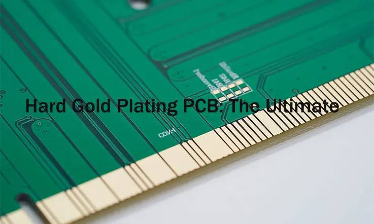
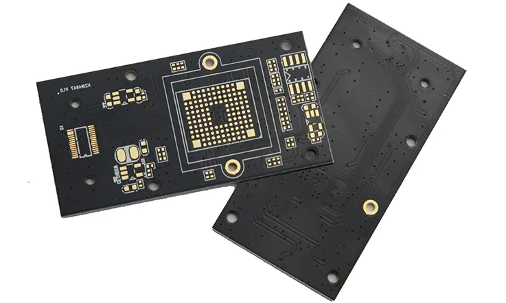
In electric circuit design, establishing reliable PCB connections is crucial to ensure proper functionality. Hard gold PCBs offer a unique solution to address this challenge by facilitating repetitive installation and removal of PCBs in complex applications. These PCBs ensure a smooth connection at the edge interface.
The implementation of hard gold PCBs brings numerous benefits that significantly enhance their effectiveness. If you are unfamiliar with this reliable PCB solution, Jarnistech is here to provide you with valuable insights. As a trusted manufacturer of hard gold PCBs, we offer high-quality solutions tailored to meet your specific requirements.
Our comprehensive FAQ guide covers all the essential information about hard gold PCBs, allowing you to understand their intricacies and make informed decisions. With our expertise and dedication to excellence, we ensure that your PCB needs are met with the utmost professionalism.
Partnering with Jarnistech empowers you to leverage the advantages of hard gold PCBs and optimize your circuit design. Contact us today to discover how our reliable PCB solutions can enhance your projects.
What is A Hard Gold Plating PCB ?
A hard gold plating PCB refers to a printed circuit board that has undergone a process called hard gold plating on its surface. Hard gold plating is a type of electroplating process where a layer of gold is deposited onto the surface of the PCB to enhance its performance, durability, and conductivity.
In hard gold plating, a layer of hard gold alloy (usually a combination of gold and other metals like cobalt or nickel) is selectively deposited onto specific areas of the PCB, typically the contact pads and connectors. This hard gold layer acts as a protective coating, ensuring reliable electrical connections, resistance to wear, and corrosion resistance.
The main purpose of hard gold plating on a PCB is to improve the conductivity and durability of the contact areas. It helps maintain low electrical resistance, allowing for efficient signal transmission and reducing the risk of defects such as oxidation or tarnishing. The hard gold plating also provides a robust surface for soldering and wire bonding processes, ensuring secure and reliable connections between components.
How Many Types of Hard Gold Plating PCB ?
There are typically two types of hard gold plating used on printed circuit boards (PCBs):
Electrolytic Hard Gold Plating: This method involves electroplating a layer of hard gold onto the PCB’s surface. It provides a thick and durable coating, usually ranging from 30-50 micro-inches (0.75-1.25 micrometers) in thickness. Electrolytic hard gold is commonly used for applications where repeated physical contact or environmental factors may cause wear or corrosion.
Electroless Hard Gold Plating: In this process, a layer of hard gold is deposited onto the PCB using a chemical reaction, without the need for an electric current. Electroless hard gold plating typically results in a thinner coating, typically ranging from 3-8 micro-inches (0.075-0.2 micrometers) in thickness. It offers good solderability and is often used in applications where cost and space constraints are important.
What Is The Recommended Thickness Of PCB Hard Gold Plating ?
The recommended thickness of PCB hard gold plating can depend on various factors, including the application requirements and specific industry standards. However, the typical range for hard gold plating thickness is as follows:
Electrolytic Hard Gold Plating: The thickness for electrolytic hard gold plating typically falls between 30 to 50 micro-inches (0.75 to 1.25 micrometers). This thickness range provides a durable and reliable gold coating suitable for applications that involve repeated physical contact or exposure to harsh environments.
Electroless Hard Gold Plating: For electroless hard gold plating, the recommended thickness is generally thinner, ranging from 3 to 8 micro-inches (0.075 to 0.2 micrometers). This thinner gold layer still offers good solderability and corrosion resistance while being more cost-effective compared to thicker gold coatings.
It’s crucial to consider the specific requirements of your PCB design and the intended application when determining the appropriate thickness for hard gold plating. It’s recommended to consult with the manufacturer or adhere to relevant industry standards (such as IPC-4552) to ensure the selected gold thickness meets the desired performance and reliability criteria.
Which Are The Design Rules For Hard Gold Plating PCB ?
The design rules for hard gold plating on PCBs can vary depending on the specific requirements of the application and the capabilities of the manufacturer. However, some general guidelines include:
Gold Pad Size: The gold pad should be larger than the corresponding component lead or contact pad to ensure proper coverage and contact reliability.
Gold Thickness: The desired gold thickness should be specified, typically ranging from 30-50 micro-inches (0.75-1.25 micrometers) for electrolytic hard gold and 3-8 micro-inches (0.075-0.2 micrometers) for electroless hard gold.
Keep-out Areas: Design the PCB layout to have keep-out areas around gold-plated pads to prevent solder mask or other materials from encroaching on the gold surface.
Rounding Corners: It is recommended to round the corners of gold pads to enhance the durability of the gold-plated surface and minimize stress concentration.
Via Placement: Avoid placing vias directly on gold pads since the plating process may not adequately cover the via, leading to potential reliability issues.
Silk Screen Printing: If necessary, ensure that the silk screen printing is properly aligned with the gold pads to avoid any overlap or interference.
It’s important to note that these are general guidelines, and it’s always advisable to consult with the manufacturer or PCB designer to obtain specific design rules and recommendations for the intended gold plating process and application.
How Do You Perform PCB Hard Gold Plating ?
The process of PCB hard gold plating typically involves the following steps:
Surface Preparation: The PCB undergoes thorough cleaning to remove any dirt, oils, or contaminants from the surface. This is typically done through a combination of mechanical scrubbing, chemical cleaning, and rinsing processes.
Electroless Nickel Plating: Before applying the gold layer, an electroless nickel (EN) plating is usually applied to the PCB surface. This involves immersing the PCB in a bath containing a solution of nickel salts and reducing agents. The EN plating creates a thin layer of nickel on the surface, providing good adhesion and a barrier between the base material and the gold.
Activation: After the EN plating, the PCB is selectively activated using an acidic solution or proprietary activation chemical. This prepares the surface for effective gold adhesion and improves the overall bonding strength.
Gold Plating: Once activated, the PCB is immersed in the gold plating solution. The gold plating process can be carried out using either electrolytic or electroless methods, depending on the specific requirements and desired results.
● Electrolytic Hard Gold Plating: In this method, the PCB is placed as the cathode in an electrolytic cell containing a gold salt solution. An appropriate voltage and current are applied, allowing the gold ions to be reduced and deposited onto the PCB surface.
● Electroless Hard Gold Plating: In this method, the PCB is immersed in an electroless gold bath containing a reducing agent. The gold deposition occurs through an autocatalytic process without the need for an external power supply.
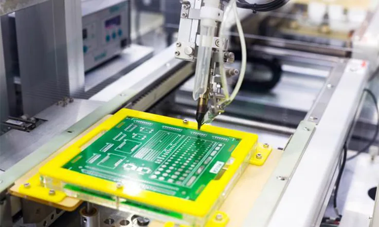
Post-treatment and Quality Control: After the gold plating process, the PCB is thoroughly rinsed to remove any residual chemicals and dried. Post-treatment steps may include applying a protective coating or additional surface finishes to ensure the longevity and reliability of the hard gold plating.
Throughout the entire process, various quality control measures are implemented to check the thickness, adhesion, and overall quality of the hard gold plating. These can include visual inspection, X-ray fluorescence (XRF) testing, cross-section analysis, and adhesion tests.
It’s important to note that the specific details and parameters of the PCB hard gold plating process can vary based on the manufacturer’s capabilities, customer requirements, and industry standards.
Why Should You Choose Hard Gold Plating PCB ?
There are several reasons why you should choose hard gold plating for PCBs:
Durability: Hard gold plating provides excellent durability and wear resistance, making it suitable for applications that involve frequent insertion and removal of connectors or components. It can withstand repeated cycles without significant degradation, ensuring long-lasting performance.
Corrosion Resistance: Hard gold plating offers superior resistance to corrosion and tarnishing compared to other plating options. This is especially beneficial in environments with high humidity, moisture, or exposure to harsh chemicals, where it helps protect the PCB contacts and ensure reliable performance over time.
Enhanced Electrical Conductivity: Hard gold plating exhibits excellent electrical conductivity, which is essential for applications that require low resistance and reliable signal transmission. It helps maintain signal integrity, reduce electrical losses, and ensure proper functioning of the PCB.
Solderability and Wire Bonding: The smooth and stable surface of hard gold plating facilitates soldering processes, allowing for reliable and consistent solder joints. It also provides a suitable surface for wire bonding, enabling secure and robust connections between components.
Contact Reliability: Hard gold plating ensures reliable and stable electrical contacts between components and PCB traces. It minimizes contact resistance, reducing the risk of intermittent connections or signal disruptions. This is particularly important in high-frequency applications or those that demand precise and consistent signal transmission.
Compatibility with Industry Standards: Hard gold plating is a widely accepted and recognized plating option in the PCB industry. It conforms to industry standards and specifications, ensuring compatibility with other manufacturing processes and ease of integration into existing production workflows.
Longevity and Shelf Life: PCBs with hard gold plating have a longer lifespan compared to other surface finishes. The durability and corrosion resistance of hard gold plating contribute to the overall longevity of the PCB, making it a reliable choice for critical or long-lasting applications. Additionally, the gold plating helps preserve the integrity of the PCB during storage or periods of inactivity.
Considering these factors, choosing hard gold plating for PCBs can provide you with a reliable, durable, and long-lasting solution that ensures optimal electrical performance and contact reliability.
What Are The Limitations Of Hard Gold PCB ?
Hard gold plating on PCBs offers several advantages, but it also has some limitations to consider:
Cost: Hard gold plating is generally more expensive than other surface finishes used on PCBs, such as HASL (Hot Air Solder Leveling) or ENIG (Electroless Nickel Immersion Gold).
Thickness Control: Achieving precise and uniform gold thickness during plating can be challenging. Variations in thickness may occur, leading to potential issues with solderability and contact reliability.
Surface Smoothness: Hard gold plating tends to have a rougher surface compared to other finishes like ENIG. This roughness can impact the insertion and withdrawal forces of connectors and may require additional measures for smooth mating.
Solderability: Excessive gold thickness or rough surface texture can adversely affect the ability of solder to wet the gold surface, leading to solder joint issues or reduced solderability.
Wear Resistance: While hard gold offers good wear resistance, it is not suitable for highly demanding applications where extreme wear or abrasion is expected. In such cases, other specialized coatings like electroless nickel with immersion gold (ENIG) or electroless nickel with hard gold may be more appropriate.
Environmental Considerations: Hard gold plating typically involves the use of cyanide-based solutions, which present environmental challenges and require proper waste management and disposal practices.
Despite these limitations, hard gold plating remains a popular choice for specific applications that require durable contact surfaces or superior corrosion resistance. It’s crucial to carefully evaluate the requirements of the PCB design and application to determine if the benefits of hard gold plating outweigh the associated limitations and costs.
What Is The Difference Between Full Body Vs. Selective Hard Gold Plating PCB ?
Full body hard gold plating is not commonly chosen as a PCB surface finish. In this approach, the entire circuit board body is plated with hard gold either through an electrolytic procedure or immersion operation based on the PCB design. However, it is important to note that full body hard gold plating can result in poor solderability, requiring the use of highly active flux for efficient soldering to the circuit board pad.
On the other hand, selective hard gold PCB plating involves applying hard gold plating only to specific sections of the printed circuit board. The process for selective gold plating is similar to full body hard gold plating, but it requires additional masking. While this incurs additional labor costs, it can offset the expense of hard gold plating PCB material.
It should be emphasized that both full body hard gold plating and selective gold plating have their advantages and considerations depending on the specific needs of the application. Selective gold plating, with its masking requirement, can help reduce material costs, while full body hard gold plating provides a uniform hard gold plating across the entire PCB surface. Ultimately, choosing the appropriate plating method requires careful evaluation of factors such as solderability requirements, cost considerations, and overall design objectives.
Hard Gold Plating and Soft Gold Plating PCB: Which one is Better ?
Hard Gold Alloy Plating: This type of hard gold plating involves depositing a layer of gold alloy onto the PCB surface. The gold alloy is typically a combination of gold with other metals like nickel or cobalt. The addition of these metals enhances the hardness, wear resistance, and durability of the gold plating.
Soft Gold Plating with Gold Flash: Soft gold plating refers to the deposition of a layer of pure gold onto the PCB surface. While it is called “soft gold,” it still provides a certain level of hardness compared to other plating options. In some cases, a gold flash layer, which is an extremely thin layer of gold, is deposited before the soft gold layer to improve surface conductivity and prevent oxidation.
The choice between hard gold alloy plating and soft gold plating with gold flash depends on the specific requirements and preferences of the application. Hard gold alloy plating is generally preferred when additional durability and wear resistance are essential, particularly in applications with high insertion/removal cycles or harsh environments. Soft gold plating with gold flash may be used when the focus is on achieving high electrical conductivity and maintaining a pure gold surface.
It’s important to note that the selection of the appropriate type and thickness of gold plating for a PCB depends on various factors such as the application requirements, industry standards, and cost considerations.
Is Hard Gold PCB Plating Better Than ENIG Plating ?
The choice between hard gold plating and ENIG (Electroless Nickel Immersion Gold) plating depends on the specific requirements of the application. Both plating options have their advantages and considerations. Here’s a comparison of hard gold plating and ENIG plating:
Hard Gold Plating:
Advantages:
Durability: Hard gold plating offers superior durability and wear resistance, making it suitable for applications with frequent connector insertions and removals.
Corrosion Resistance: Hard gold plating provides excellent resistance to corrosion and tarnishing, making it suitable for harsh environments or applications exposed to moisture and chemicals.
Contact Reliability: Hard gold plating ensures reliable and stable electrical contacts, minimizing contact resistance and reducing the risk of intermittent connections or signal disruptions.
Solderability: Hard gold plating provides a stable and reliable surface for soldering processes, facilitating secure solder joints and good solderability.
Considerations:
Cost: Hard gold plating is generally more expensive than ENIG plating due to the additional metals used in the gold alloy.
Thickness Limitations: Hard gold plating may have limitations regarding thickness, limiting applications that require thicker plating for specific requirements.
ENIG (Electroless Nickel Immersion Gold) Plating:
Advantages:
Flat Surface: ENIG plating provides a flat and even surface, which is beneficial for applications with fine-pitch components and surface mount technology (SMT).
Excellent Solderability: ENIG plating offers excellent solderability, allowing for reliable solder joints and high-quality solder connections.
Corrosion Resistance: ENIG plating provides good resistance to corrosion and oxidation, ensuring long-term reliability and protection of PCB contacts.
Considerations:
Wear Resistance: ENIG plating is generally less wear-resistant compared to hard gold plating and may not be suitable for applications subject to frequent connector insertions and removals.
Contact Reliability: While ENIG plating offers good contact reliability, hard gold plating may have an edge in terms of long-term stability and reduced contact resistance.
Cost: ENIG plating is typically less expensive than hard gold plating, making it a more cost-effective option for certain applications.
In summary, neither hard gold plating nor ENIG plating is universally “better” than the other. The choice depends on specific application requirements, including factors such as durability, wear resistance, cost, solderability, and contact reliability. Evaluating these factors will help determine the most suitable plating option for a given application.
What Are The IPC Standards For Hard Gold Plating PCB ?
The IPC standards for PCB hard gold plating encompass several key considerations:
Chemical Composition: To ensure optimum durability and stiffness of PCB contact edges, hard gold plating should consist of 5-10 percent cobalt.
Thickness: The plating thickness of gold fingers typically falls within the range of 2-50 microinches. Standard thicknesses include 0.125 inches, 0.093 inches, 0.062 inches, and 0.031 inches. Thinner thicknesses are commonly used for hard gold plating PCB prototypes, while greater thicknesses are applied to connecting edges that undergo frequent insertion and removal.
Visual Test: Gold fingers of hard gold plated PCBs must pass a visual inspection using a magnifying lens. This test ensures that the edges possess a polished, clean surface, free from excessive gold plating or visible traces of nickel.
At JarnisTech, we provide a diverse range of hard gold plating PCBs tailored to meet your specific requirements and specifications. Our offerings are designed to adhere to IPC standards and deliver high-quality performance.
Contact us today to discuss your hard gold plating PCB needs and benefit from our reliable solutions and expertise.
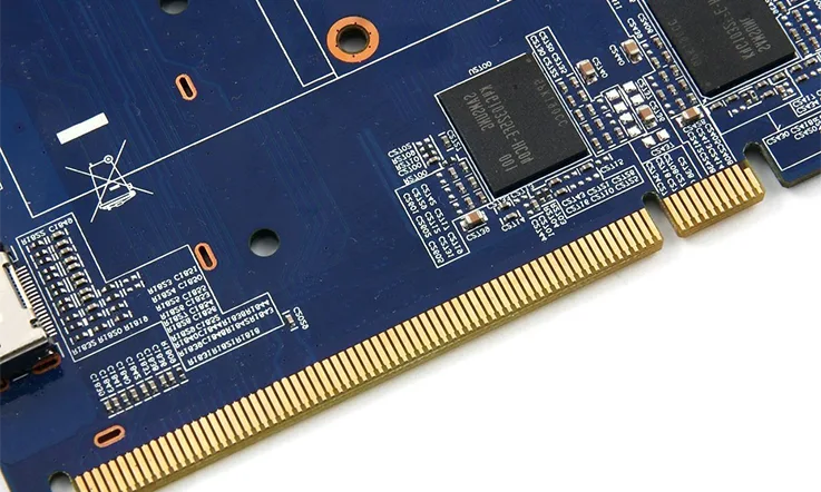
Why Must You Plate PCB Fingers With Hard Gold ?
PCB (Printed Circuit Board) fingers are plated with hard gold for several reasons:
Durability: Hard gold plating provides a thick and durable layer on the PCB fingers, making them resistant to wear and corrosion caused by repeated insertions and removals in connectors. This is especially important for connectors that are frequently utilized or in harsh environments.
Reliable electrical performance: The hard gold layer ensures a consistent and reliable electrical connection between the PCB and mating connectors. It has low contact resistance, excellent conductivity, and is less prone to oxidation compared to other plating materials.
Protection against contamination: Hard gold plating acts as a barrier against contaminants such as dust, dirt, and moisture that can accumulate on the PCB fingers. This helps to maintain reliable electrical contact and prevents signal degradation or intermittent connections.
Compatibility: Hard gold is compatible with a wide range of mating connector materials, ensuring good compatibility and reducing the risk of galvanic corrosion when connecting different metals.
Overall, hard gold plating on PCB fingers ensures long-term reliability and excellent performance in connectors by providing durability, reliable electrical connections, protection against contamination, and material compatibility.
How Can You Choose The Best Manufacturer Of Hard Gold PCB ?
Before selecting a manufacturer for your hard gold PCB needs, it is essential to consider key factors that contribute to a successful partnership:
Extensive Experience: Look for a manufacturer with long-term experience in hard gold PCB manufacturing. This expertise ensures a deep understanding of the process and the ability to deliver high-quality results consistently.
Reliable Raw Material Storage: Adequate storage of quality raw materials is crucial for producing reliable hard gold PCBs. Ensure the manufacturer maintains a well-managed inventory of essential materials to meet your project requirements.
Skilled and Well-Equipped Team: A professional team of experts is vital for manufacturing top-notch hard gold PCBs. Verify that the manufacturer possesses a skilled workforce with technical proficiency and modern equipment to handle the production process effectively.
Responsive Customer Service: Choose a manufacturer that provides 24/7 customer service and actively supports you throughout the assembly and fabrication stages. A responsive and supportive team can address any concerns or queries promptly, leading to smoother project execution.
Performance Testing Facility: A manufacturer with a well-equipped performance testing facility can ensure the reliability and functionality of your hard gold PCBs. Thorough testing helps identify and rectify any potential issues before the products reach you.
Production Capacity and Quality Certification: It’s advantageous to collaborate with a manufacturer that has a considerable production capacity and holds relevant certifications such as ISO. This demonstrates their ability to handle large-scale orders and meet stringent quality standards, like IPC Class 2 or Class 3.
JarnisTech stands out as a leading manufacturer of hard gold PCBs, leveraging over 20 years of industry experience. We offer reliable and trustworthy PCB manufacturing services, ensuring products of superior quality. Contact us now to experience effective PCB solutions manufactured to the rigorous standards of IPC Class 2.
Summary
Hard gold PCBs have revolutionized circuit design by offering remarkable effectiveness. These boards provide an efficient solution to prevent edge problems, allowing for frequent PCB usage through hard gold plating.
At Jarnistech, we understand the significance of choosing the right PCB for your needs. We are committed to providing you with the utmost satisfaction and a superior PCB experience. Our comprehensive FAQ guide provides detailed and easy-to-understand information about Hard gold circuit boards, ensuring that you have a clear understanding of their advantages and applications.
We aim to offer you peace of mind by equipping you with the knowledge necessary to make informed decisions. If you have any further inquiries or require additional assistance, our dedicated team is readily available to provide prompt and reliable support.
Partner with Jarnistech to benefit from our expertise and access the most effective PCB solutions on the market. Contact us today to begin your journey towards optimal circuit design.
Related Posts:
PCB Surface Finish& Series
3.Lead Free HASL PCB Surface Finish
4.Immersion Gold PCB Surface Finish
5.Gold Plating PCB Surface Finish
6.Immersion Silver PCB Surface Finish
7.Immersion Tin PCB Surface Finish
8.Nickel Plating PCB Surface Finish
9.Immersion Nickel PCB Surface Finish
10.Hard Gold PCB Surface Finsh
11.Sort Gold PCB Surface Finish