
Metal Core Printed Circuit Boards (MCPCBs) are a foundational technology in modern electronics where effective thermal performance and power density are defining considerations. This guide journeys through the intricacies of MCPCB engineering, covering material selection and thermal design, through to manufacturing principles (DFM), specialized assembly, and robust reliability testing. We’ll also explore best practices for high-current/voltage scenarios, adherence to industry standards, and the diverse applications in fields like LED lighting and electric vehicles. Our intention is to equip you with the understanding to fully leverage metal core technology, helping you achieve excellent performance, durability, and manufacturability for your advanced electronic systems.
Understanding Metal Core PCBs and Their Value in Heat-Sensitive Applications
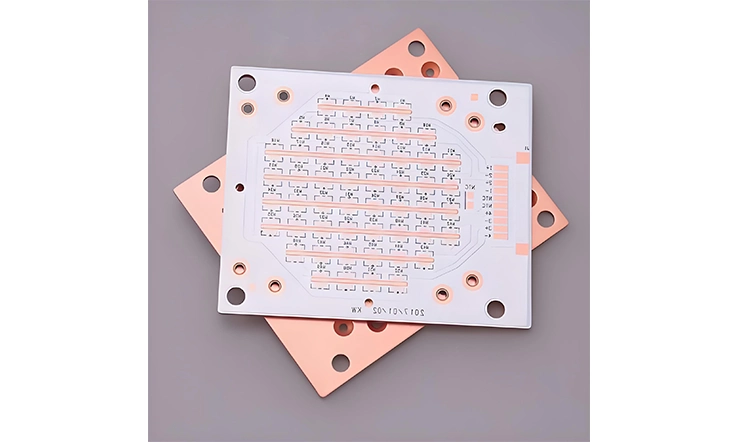
Metal Core Printed Circuit Boards provide a distinct solution for thermal management within electronic assemblies. Unlike conventional FR4 boards, MCPCBs integrate a metal substrate—typically aluminum or copper—to markedly improve heat dissipation. This construction effectively manages the heat generated by devices such as LED lighting modules, power electronics, and industrial machinery control systems.
Removing heat efficiently from sensitive electronic components is necessary to prevent performance degradation or operational failure. The metal core acts as a thermal conductor, distributing heat more uniformly and helping to avert localized high-temperature areas. This characteristic enhances the durability and reliability of electronic devices, particularly those subjected to heavy electrical loads or operating in high-temperature environments. You’ll find this leads to more dependable products with longer operational lives.
Furthermore, the combination of a metal substrate with specialized dielectric layers provides electrical insulation while facilitating effective thermal transfer. This balance allows designers to optimize circuit performance, uphold operational safety, and extend device lifespan—a synergy often realized most effectively when working with manufacturing partners who grasp these nuances.
MCPCB vs. FR4: A Look at Thermal Performance
Traditional FR4 PCBs have long been used in the electronics industry for their mechanical stability and electrical insulation properties. However, their limited thermal conductivity can present challenges in managing heat for high-power applications. Metal Core PCBs, in contrast, offer several advantages:
| Feature | Standard FR4 PCB | MCPCB with Aluminum Core | MCPCB with Copper Core |
| Thermal Conductivity (W/m·K) | ~0.25 | 1.0 – 9 | 3.5 – 9 |
| Typical Dielectric Thickness (mm) | 0.1 – 0.2 | 0.03 – 0.12 | 0.03 – 0.10 |
| Thermal Resistance (°C/W) | High | Medium | Low |
| Heat Transfer Efficiency | Low | Medium–High | High |
| Recommended Applications | Consumer electronics | LED lighting, power ICs | High-power inverters |
●They provide significantly improved thermal conductivity, often several times higher than that of FR4. This means heat moves away from your components much more readily.
●This advantage stems from the metal substrate’s capacity to rapidly transfer heat away from concentrated heat sources.
●The dielectric material positioned between the metal base and copper layers contributes substantially to this system; it must permit efficient heat transfer while ensuring robust electrical isolation. The careful selection and precise application of this dielectric are where true manufacturing craft becomes apparent.
Due to these attributes, MCPCBs are favored for applications where managing junction temperature directly influences performance and component longevity, such as in LED drivers and power converters.
Industries Leveraging Metal Core PCB Technology
The unique thermal management properties of MCPCBs appeal to various industries aiming to improve product reliability and operational efficiency. Examples include:
1. LED Lighting:
Manufacturers use metal core boards to sustain consistent brightness and prevent color shifts that can arise from heat accumulation. The longevity of LEDs is also notably extended through better thermal regulation, giving end-users a more consistent and lasting product.
2. Power Electronics:
In applications with substantial currents and voltages, MCPCBs assist in managing thermal loads, maintaining temperatures within safe operational ranges for components like MOSFETs, IGBTs, and power modules. This helps ensure these powerful systems operate as intended.
3. Industrial Equipment:
Manufacturers integrate MCPCBs to help machinery controls endure demanding thermal conditions, contributing to operational stability and reducing instances of premature system failure in thermally challenging settings. The result is more uptime and less maintenance.
4. Automotive Sector:
Particularly in electric vehicles (EVs) and advanced driver-assistance systems (ADAS), MCPCBs are used for battery management (BMS), on-board chargers, LED headlights, and inverter boards to meet stringent thermal and electrical requirements. This contributes to the safety and reliability expected in automotive applications.
Material Properties and the Science of Heat Dissipation
The performance characteristics of MCPCBs are largely determined by the interaction between the metal core and the dielectric layer.
1. Metal Core Materials: Metals like aluminum and copper are selected for the core due to their excellent thermal conductivity and mechanical strength.
●Aluminum presents a good combination of cost-effectiveness, lighter weight, and efficient thermal transfer, making it a popular choice.
●Copper, while offering superior conductivity, involves more intricate manufacturing processes and typically comes at a higher cost. Choosing the right core material often depends on application-specific thermal demands and manufacturing considerations. Sound advice during the design phase can streamline development and ensure optimal material compatibility for subsequent assembly processes, a conversation we find always benefits the final product.
2 .Dielectric Layer: The dielectric material is precisely formulated to deliver effective electrical isolation with the lowest achievable thermal resistance.
●The expertise in applying these dielectric layers uniformly and to exact thickness specifications is a component of high-quality MCPCB fabrication and assembly, directly impacting performance and reliability.
●Its thickness and composition directly affect the board’s overall efficiency in transferring heat. While thinner dielectric layers improve thermal conduction, they demand high precision during manufacturing to prevent electrical breakdown under voltage stress. Producing dependable MCPCBs with these features requires advanced manufacturing capabilities.
Selecting Core Materials: Aluminum, Copper, and Hybrid Composites
Choosing the appropriate core material is a foundational step in metal core PCB design. The metal substrate directly influences the board’s thermal management, mechanical strength, and overall reliability. Among the options, aluminum and copper are frequently utilized, each bringing distinct properties that affect heat conduction and manufacturability. Beyond these, hybrid composites are also available as innovative alternatives, combining traits to address specific application needs.
Understanding the nuanced differences between materials like aluminum and copper helps engineers balance cost, weight, and thermal performance. Concurrently, the selection of the dielectric layer and appropriate substrate thickness also shapes the efficiency of heat transfer and electrical insulation, tailoring the PCB to the unique demands of power electronics, LED lighting systems, and industrial machinery. Making informed choices in these areas, often with guidance from experienced manufacturing partners, is beneficial for achieving excellent device performance and assembly efficiency. We’ve seen firsthand how this collaborative approach leads to smoother project execution.
Comparative Analysis: Aluminum vs. Copper Core
When selecting a metal core, aluminum and copper present different advantages:
1. Aluminum Cores:
●Offer a favorable combination of affordability, light weight, and effective thermal conductivity.
●Their ability to spread heat across the PCB surface helps reduce localized heating, which can enhance component longevity.
●Aluminum’s good machinability and widespread availability often make it a preferred choice for many high-volume manufacturing scenarios
2. Copper Cores:
●Provide higher thermal conductivity, enabling faster and more efficient heat dissipation.
●This makes copper-based MCPCBs especially suitable for applications where thermal loads are intense and maintaining temperature stability is a primary concern.
●However, copper’s greater density and typically higher cost can influence design decisions, often reserving its use for specialized or high-performance products.
The choice between aluminum and copper substrates depends on multiple factors. These include the thermal profile of the device, mechanical requirements, production budgets, and even the specific assembly processes planned. It’s about finding the right fit for your specific situation.
Dielectric Layer Considerations and Thermal Resistance
The dielectric layer is a non-conductive material that separates the metal core from the circuit traces. It serves the dual purpose of providing electrical insulation and facilitating thermal conduction from the circuit to the core. Its composition and thickness significantly affect the PCB’s capacity to transfer heat effectively while maintaining robust electrical isolation.
●Thermal Resistance: Materials with lower thermal resistance support more efficient heat flow from heat-generating components into the metal core. This thermal behavior directly affects junction temperatures in applications such as LEDs and power converters, influencing both energy performance and the duration over which these devices remain within their intended operating parameters.
●Thickness and Precision: Thinner dielectric layers generally improve thermal conductivity. However, they require precise manufacturing controls and high-quality materials to maintain electrical safety margins and long-term reliability. Achieving this balance consistently is a hallmark of fabricators who truly understand these materials.
●Other Properties: Designers also consider factors such as the dielectric breakdown voltage (its ability to withstand high voltages), mechanical flexibility (should the application require it), and compatibility with various surface finishes used in PCB assembly.
Balancing these properties ensures the PCB meets its operational requirements and supports long-term durability in its intended environment, giving you confidence in the final product.
Choosing the Right Substrate Thickness
The thickness of the metal substrate has a considerable impact on both thermal management and mechanical stability.
| Substrate Thickness (mm) | Typical Application Examples | Heat Spreading Capability | Mechanical Rigidity | Weight Impact |
| 0.8 – 1.0 | Compact LED modules, wearable tech | Moderate | Flexible | Minimal |
| 1.2 – 1.6 | General-purpose LED drivers, IoT | Good | Balanced | Light–Moderate |
| 2.0 – 2.5 | Power converters, sensor boards | Strong | Rigid | Moderate |
| 3.0+ | EV inverters, industrial machinery | Excellent | Very rigid | Heavier |
1. Thermal Performance: Thicker metal cores typically enhance heat spreading across the PCB. This helps mitigate hotspots by distributing thermal loads more evenly, which can be advantageous for components with high heat output.
2. Mechanical Aspects: Increased thickness also adds to the rigidity of the board. Conversely, it may add to the overall weight and could influence board flexibility, which are considerations for the final product design.
3. Application-Specific Needs: Selecting the optimal thickness involves assessing the thermal demands of the application, the physical constraints of the device, and the capabilities of the manufacturing process.
●For instance, LED lighting modules designed for compact spaces might prioritize thinner, lighter substrates.
●In contrast, industrial control boards intended for harsher environments might benefit from thicker, more robust cores.
This decision is often part of an iterative design process. This can involve thermal simulations during the design phase, prototyping to validate choices, and real-world testing to ensure the MCPCB achieves a balanced performance tailored to the application. It’s a journey of refinement we’re familiar with.
Designing for Thermal Efficiency: Stackup, Vias, and Heat Spreading
Effective thermal management within metal core PCBs depends significantly on how the layers are arranged (the stackup), how heat is transferred through structures like vias, and how the board’s overall architecture promotes the even distribution of temperature. Thoughtful design choices in stackup configuration and the creation of thermal conduction paths directly influence how well heat moves away from sensitive components. This, in turn, impacts device durability and operational stability.
By optimizing these factors, human can better address the challenges posed by high power density and continuous operation. These are common conditions in sectors like LED lighting, power conversion, and industrial control systems, where sustained or excessive heat can affect performance and shorten the lifespan of the product. Achieving these optimizations often involves a close understanding of not just design principles but also the manufacturing capabilities that bring them to life, ensuring theory translates into tangible results.
Thermal Vias, Pads, and Relief Techniques
Several features are incorporated into MCPCB designs to manage heat flow from components to the metal core:
Thermal Vias:
●These act as small conduits, specifically designed to channel heat from surface-mounted components down through the PCB layers and into the metal core. The effectiveness of thermal vias in transferring heat is determined by their size, number, placement, and the quality of their construction during fabrication (e.g., drilling and plating). Well-executed vias make a noticeable difference.
Thermal Pads:
●Complementing vias, thermal pads are areas of copper, often larger than standard component pads, designed to provide an increased surface area for contact. This helps in drawing heat away from a component and dissipating it more evenly into a larger section of the board or directly to the metal core.
Thermal Relief Techniques:
●These involve specific pad and via designs intended to manage thermal stress. For instance, thermal relief pads connect a component lead to a copper plane using short traces (spokes) rather than a full connection. While seemingly counterintuitive for heat transfer, these strategies help reduce mechanical stress concentrations that can occur during temperature cycling (heating and cooling). This, in turn, supports the longevity of solder joints and the integrity of surface finishes.
| Feature | Typical Specification | Functionality in Thermal Management | Design Note |
| Thermal Via Diameter | 0.2 – 0.5 mm | Allows heat transfer from surface to metal core | Use arrays near heat sources for better dissipation |
| Via Pitch | 0.8 – 1.2 mm | Controls density of heat conduction paths | Closer pitch improves heat extraction efficiency |
| Copper Fill in Via | 90%–100% (plated/filled) | Increases thermal conductivity of the via | Fully filled vias perform better than tented/empty ones |
| Thermal Pad Area | >2× component footprint | Provides larger surface for heat draw | Combine with multiple vias for maximum impact |
| Thermal Relief Spoke Width | 0.25 – 0.5 mm | Controls current & heat flow from pad to plane | Balances soldering ease with mechanical stress relief |
Proper implementation of these techniques is a blend of good design practice and precise manufacturing execution.
Multilayer MCPCBs: Power Distribution and EMI Considerations
Modern metal core PCBs often feature multiple layers to achieve a balance between thermal management and complex electrical performance requirements. A multilayer stackup offers several benefits:
●Dedicated Power and Ground Planes: It allows for the segregation of power and ground planes from signal layers. This facilitates cleaner power distribution to components and can improve signal integrity by providing stable reference planes and reducing electrical noise.
●Electromagnetic Interference (EMI) Mitigation:In addition to thermal concerns, electromagnetic interference can pose challenges in densely packed circuits. The strategic arrangement of layers, careful grounding schemes, and the shielding effect of planes within multilayer MCPCBs can help lessen EMI effects. This contributes to more stable operation, which is particularly beneficial in sensitive industrial environments and complex electronic assemblies.
The fabrication of reliable multilayer MCPCBs requires advanced manufacturing processes to ensure proper layer registration, via formation, and dielectric integrity.
Simulation Tools for Predictive Thermal Modeling
Before committing to physical prototyping, thermal simulation tools offer valuable insight into how heat is likely to behave within a given MCPCB design. These software solutions enable engineers to:
●Model Heat Flow: They can simulate the flow of heat through the various parts of the PCB, including the metal substrate, dielectric layers, vias, and copper traces.
●Anticipate Hotspots: This allows for the anticipation of potential high-temperature areas (hotspots) on the board under operational loads.
●Optimize Layouts: Based on simulation results, layouts can be optimized to improve heat spreading and reduce peak temperatures before any physical boards are made.
Using simulation effectively helps to reduce the need for multiple costly trial-and-error prototyping cycles. It enables design refinements that enhance thermal performance and overall product reliability, leading to a more robust outcome with fewer surprises.
High Current and High Voltage Design Rules in MCPCB
Designing metal core PCBs for applications that handle elevated currents and voltages demands careful adherence to established electrical and mechanical principles. Ensuring reliable performance and operational safety in power electronics or industrial equipment requires precise control over conductor dimensions, isolation distances, and the board’s ability to withstand environmental influences without degradation.
Attending to these aspects early in the design process helps minimize risks related to overheating, electrical breakdown, and mechanical failure. This proactive approach also accommodates the practical constraints faced by entities such as LED lighting manufacturers, heavy machinery OEMs, and power module designers. Successfully navigating these design rules often benefits from collaboration with manufacturing partners who understand how to translate design intent into a robust, reliable physical product. We find this early collaboration prevents many downstream headaches.
Trace Width and Clearance Based on IPC Standards
The dimensions of copper traces and the spacing (clearance) between them are fundamental to a PCB’s ability to manage current and withstand voltage. Industry standards, such as IPC-2152, offer guidance for calculating appropriate trace dimensions. Key considerations include:
1. Current-Carrying Capability & Trace Width:
●A broader trace generally exhibits lower electrical resistance. This reduces resistive losses and associated heat buildup, which benefits long-term reliability, especially in circuits designed to carry high currents.
●Determining the correct width involves considering the expected current load, the acceptable temperature rise for the materials and components, and the thermal dissipation characteristics of the MCPCB.
2. Voltage Withstand & Clearance:
●Adequate clearance between conductive elements (traces, pads, etc.) is necessary to prevent electrical arcing or flashover, particularly at higher voltages.
●Sufficient spacing ensures compliance with safety margins and helps maintain the integrity of the circuit over its operational life. Achieving and verifying these precise trace widths and clearances consistently requires advanced etching, imaging, and quality control processes during PCB fabrication.
| Parameter | Typical Value Range (Based on IPC-2152) | Design Implication |
| Trace Width for 10A (internal) | ~3.5 mm (35 µm copper, 10°C rise) | Prevents overheating in high-current designs |
| Trace Width for 10A (external) | ~1.5 mm (35 µm copper, 10°C rise) | Surface traces dissipate heat more efficiently |
| Minimum Clearance for ≤30V | ≥0.13 mm (per IPC-2221B Table 6-1) | Prevents arcing in low-voltage sections |
| Minimum Clearance for ≥300V | ≥2.5 mm (basic), ≥5.0 mm (reinforced) | Required for high-voltage isolation to prevent flashover |
| Copper Thickness Options | 35 µm (1 oz), 70 µm (2 oz), 105 µm (3 oz), etc. | Impacts current capacity and thermal resistance |
These parameters must always be considered alongside the PCB’s overall thermal design to strike an effective balance between electrical performance and efficient heat dissipation.
High Voltage Isolation: Arc Prevention and Safety Measures
In metal core PCB layouts where high voltage circuits operate near sensitive low-voltage sections, maintaining sufficient electrical isolation is a primary design objective. Several factors contribute to preventing arc formation, which can lead to catastrophic failure:
●Dielectric Material Properties: The choice of dielectric materials, their thickness, and their intrinsic insulating capabilities are foundational to high-voltage performance.
●Creepage and Clearance Distances: Designers must ensure adequate distances over surfaces (creepage) and through air (clearance) between conductors at different potentials.
●Protective Coatings and Treatments: Conformal coatings or other surface treatments can enhance insulation and protect against environmental factors like moisture or contaminants that might reduce isolation effectiveness.
●Reinforced Insulation Techniques:In some cases, specific design techniques or multiple layers of insulation might be employed to provide added security against voltage breakdown.
This attention to detail in isolation design safeguards not only the equipment itself but also enhances the safety of personnel who may interact with the devices. The dependability of these isolation barriers depends significantly on the quality of materials used and the precision of manufacturing processes, such as lamination and coating application.
Environmental Stress Considerations for Industrial Use
Metal core PCBs intended for industrial applications are often expected to perform reliably despite exposure to challenging environmental conditions. These can include:
●Temperature Extremes and Cycling: Boards may experience wide temperature fluctuations or rapid changes, requiring materials that can withstand such thermal stresses without losing their properties.
●Humidity and Moisture: Prolonged exposure to humidity can degrade insulating materials and promote corrosion if not properly managed.
●Vibration and Mechanical Shock: Industrial machinery can subject PCBs to significant vibration, necessitating robust mechanical design and secure component mounting.
●Chemical Exposure: Depending on the specific industrial environment, PCBs might be exposed to various chemicals, oils, or solvents.
To address these, designers and manufacturers focus on:
●Material Selection: Choosing substrates, laminates, and surface finishes that inherently resist corrosion, withstand thermal cycling, and maintain mechanical integrity over time.
●Design Robustness: Accounting for the thermal expansion coefficients of different materials to prevent delamination or cracking under stress, and ensuring components are well-supported.
Design for Manufacturability (DFM): Cost, Tolerance, and Layout Rules
Metal Core PCBs (MCPCBs) present a range of design and fabrication challenges that differ significantly from standard FR4-based boards. Beyond thermal management, manufacturability is a central consideration that shapes both the production cost and the long-term reliability of the product. For high-power LED assemblies or industrial-grade converters, a design well-prepared for manufacturing ensures fewer production bottlenecks and improved yield.
The focus during DFM for metal substrates centers around layout rules that accommodate aluminum or copper cores, mechanical processing limits, and material-specific behaviors during etching, drilling, and routing. Addressing these aspects early in the design cycle helps streamline fabrication and assembly while maintaining compliance with industry tolerances. A proactive DFM approach, ideally incorporating feedback from fabrication specialists, can lead to more efficient production and a higher quality end-product. It’s about designing with the end in mind.
DRC in Design Software for Metal Substrates
Modern PCB design software, such as Altium Designer and Cadence Allegro/OrCAD, offers design rule check (DRC) features that can be tailored for custom substrate stacks, including those used in MCPCBs. These tools provide several benefits for DFM:
●Custom Rule Configuration: They support the configuration of specific clearance rules, drill-to-copper spacing, and other layer-specific constraints that directly reflect the unique characteristics and behaviors of conductive metal cores. These rulesets are most effective when developed in consideration of, or in consultation with, a chosen fabricator’s specific capabilities.
●Substrate-Aware Checks: When working with aluminum-core, copper-core, or hybrid MCPCBs, enforcing substrate-aware rulesets helps prevent issues such as unintended copper migration, soldermask misalignments, or inconsistencies in thermal isolation.
●Accurate Modeling: Features like layer stack configuration in Altium enable accurate modeling of heat-spreading layers, while Cadence often supports dynamic constraint sets for routing over plated and non-plated areas, which is pertinent for some MCPCB constructions.
Integrating DRC from the start of the design process minimizes the need for redesign loops and helps designers anticipate areas where manufacturability might be limited by factors like material hardness or specific mechanical tooling constraints.
Copper Balancing and Thermal Stress Mitigation
Copper imbalance in MCPCBs, particularly in double-sided designs, can often result in mechanical deformation (warpage, bow, or twist) during thermal cycling. This is especially noticeable during high-temperature processes like reflow or wave soldering, amplified by the differing thermal expansion coefficients of copper, the dielectric material, and the metal core.
To reduce such phenomena, designers employ several strategies:
●Copper Balancing: This involves ensuring that different layers, or opposing sides of a double-layer MCPCB, contain roughly equal amounts of copper area and distribution.
●Dummy Copper Fills: Where functional copper is insufficient for balance, patterned non-functional (dummy) copper fills can be added to equalize the copper distribution.
●Layout Discipline: These practices help distribute heat and mechanical stress more evenly across the board, contributing to its flatness and stability.
| Layout Factor | Recommended Guideline | Design Benefit |
| Copper Area Symmetry (Top vs. Bot) | ≥ 90% match for 2-layer boards | Minimizes board warpage and bow during thermal cycles |
| Dummy Copper Density | ≥ 30% coverage in low-copper zones | Enhances structural uniformity, reduces CTE mismatch effects |
| Max Copper Thickness Difference | ≤ 0.5 oz across layers | Reduces interlayer stress and potential delamination |
| CTE (Coefficient of Thermal Expansion) | Cu: ~17 ppm/°C, Al core: ~22–24 ppm/°C | Understanding this helps in stack selection and stress modeling |
| Warpage Limit Post-Reflow | ≤ 1.5% of diagonal length (per IPC-6012) | Ensures compatibility with SMT lines and pick-and-place systems |
Furthermore, controlled copper layout also limits localized hotspots that could accelerate material fatigue or cause delamination in high-power modules. Integrating such layout discipline in the initial routing stage supports smoother transitions into volume production. This is an outcome best achieved when design considerations align with proven manufacturing practices for material handling and thermal processing.
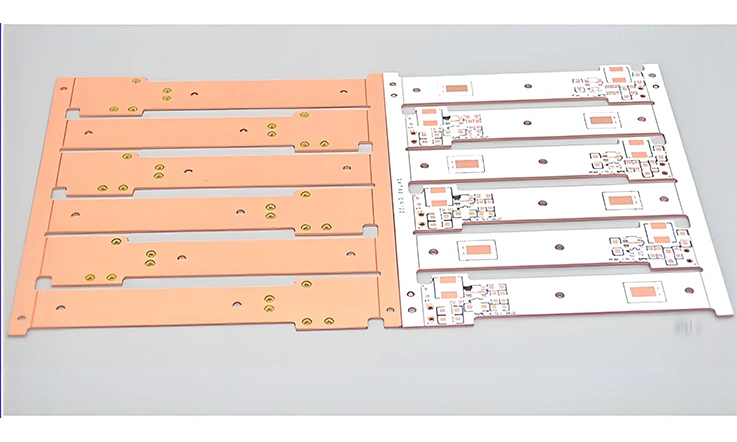
Panelization, V-Scoring, and CNC Routing Techniques
Panel design (arraying multiple PCBs onto a single manufacturing panel) for MCPCBs must reflect the unique challenges presented by their metal substrates. Unlike FR4 panels, which generally tolerate a wide range of depaneling techniques, MCPCBs demand higher mechanical precision due to their rigid cores and often thicker stackups.
Key panelization and depaneling considerations for MCPCBs include:
●Combined Techniques: Strategies typically involve a combination of V-scoring, CNC routing, and tab-routing (break-away tabs) to accommodate both the need for efficient heat conduction during processing and structural integrity during handling and assembly.
●V-Scoring: This method is commonly used to weaken the material along defined lines, simplifying board separation. However, the depth and angle of the V-score must be carefully calibrated to the core material’s hardness and thickness to ensure clean breaks and minimize tool wear.
●CNC Routing: Especially when applied to aluminum-backed MCPCBs, CNC routing often requires slower feed rates and specialized cutting bits to avoid burring, excessive tool wear, and potential substrate cracking. This demands a delicate touch.
●Panel Layout Features: Panel layouts must also incorporate space for elements like fixture holes (for securing the panel during various processes) or thermal release points to aid during any heat treatment stages of manufacturing.
Selecting the right combination of routing and scoring methods is a detailed decision. It often involves collaboration with the PCB manufacturer to optimize for their specific equipment and processes, as this directly impacts unit cost, tooling lifespan, the quality of the board edge finish, and suitability for automated assembly lines—all factors influencing production feasibility, especially for high-volume orders.
SMT & THT Assembly Guidelines for High Thermal Mass Boards
Mounting components on metal-based printed circuit boards, especially those with aluminum or copper cores, presents distinct challenges during assembly. These substrates are engineered to dissipate heat effectively, but their high thermal mass also demands thoughtful adjustments in both Surface Mount Technology (SMT) and Through-Hole Technology (THT) processes. Without tailored strategies, solder joint integrity, performance through thermal cycling, and even basic pad wetting can all be compromised.
Proper layout planning, careful reflow profile calibration, and appropriate solder material selection all contribute to achieving reliable connections. This is particularly true when dealing with high-power devices such as MOSFETs, LEDs, motor drivers, and power regulators common on MCPCBs.
Component Placement Strategies on Heat-Conductive Substrates
On aluminum or copper-backed boards, thermal behavior varies significantly depending on both component location and pad design. Unlike standard FR4, which tends to localize heat, metal core substrates rapidly spread thermal energy away from the heat source. This behavior affects temperature gradients during soldering and influences long-term component operation.
When planning the layout:
●Position High-Dissipation Parts Strategically: Components that generate significant heat (e.g., high-wattage LEDs, TO-packaged transistors) should be positioned to allow direct and efficient thermal pathways to the heat-spreading features embedded in the MCPCB stackup.
●Distribute High-Current Paths Evenly: Aim to spread out high-current traces to prevent thermal loading from concentrating excessively in one zone of the PCB, which could lead to localized overheating.
●Ensure Symmetric Pad Design: For thermally demanding components, use symmetric pad designs to avoid skewed heat sinking. Asymmetric heat withdrawal can lead to uneven mechanical stress at the solder joints over time.
For THT assemblies, especially those using thick copper pours or direct thermal paths to the metal core, hole size and plating thickness must be optimized. This ensures both robust mechanical retention and effective heat transfer. Issues like skewed hole fill or excessive voids during soldering can create hot spots and potential stress fractures after thermal cycling, challenges best addressed through precise process control during assembly.
Reflow Profile Optimization for Aluminum and Copper PCBs
The high heat capacity of metal core boards typically delays temperature ramp-up during the reflow soldering process. This necessitates modifications to standard soldering profiles that might be used for FR4 boards. A generic profile may result in insufficient wetting or cold solder joints, especially for larger components or those with substantial thermal pads.
Consider these process adjustments:
●Extended Soak Times: Longer soak periods in the reflow profile are often necessary. This allows the entire board assembly, including the thermally massive core, not just the top surface and components, to reach a uniform temperature before the solder melts.
●Controlled Ramp-Up Rates: Slower temperature ramp-up rates can help minimize the risk of warpage. This is due to the mismatch in thermal expansion rates between the metal core and the bodies of ceramic or silicon components.
●Adequate Peak Temperature Window: The peak temperature achieved during reflow, and the time spent at that temperature, must be sufficient to ensure full and reliable solder reflow across all joints. This is particularly relevant for joints located above solid metal regions of the core, which tend to absorb heat rapidly.
●Lead-Free Soldering Considerations: When using lead-free solder pastes, the process window between the solder’s melting point and the onset of rapid oxidation narrows. Utilizing oxygen-controlled reflow ovens or nitrogen-rich reflow environments can provide added process stability during these temperature transition zones.
| Reflow Profile Stage | Recommended Range (Lead-Free) | Notes for High Thermal Mass Boards |
| Ramp-Up Rate | 1–2 °C/sec | Slower ramps reduce thermal shock and warpage risks |
| Soak Zone Temp. | 150–180 °C | Ensures even heating across the MCPCB and components |
| Soak Duration | 90–120 sec | Provides time for uniform heat penetration into the metal core |
| Peak Temp. (SAC305) | 240–250 °C | Ensures full melting and wetting across thicker boards |
| Time Above Liquidus (TAL) | 45–70 sec | Sufficient to complete solder wetting without overexposure |
| Cooling Rate | 2–4 °C/sec | Controlled cooling reduces CTE-driven joint stress |
Overall, each MCPCB design, due to variations in mass, layout, and component selection, may require its own thermal profiling and validation. This detailed profiling is often performed in collaboration with an assembly house that has experience with diverse MCPCB materials, thicknesses, and application requirements, such as those for high-power LED modules, automotive DC-DC converters, or industrial AC switching units with large surface-mounted packages.
Thermal Expansion and Solder Joint Reliability
One of the significant mechanical challenges with metal-based substrates arises from the coefficient of thermal expansion (CTE) mismatch between the metal core (e.g., aluminum or copper) and the mounted components (e.g., ceramic packages, silicon dice, glass-filled epoxy bodies). For instance, aluminum expands and contracts more significantly with temperature changes than many common component materials. Over repeated thermal cycles, this difference in movement introduces mechanical tension and strain at the solder joint interface.
To mitigate these effects and enhance long-term solder joint reliability:
●Utilize Low-Stress Solder Alloys: Employ solder alloys specifically formulated for enhanced ductility and fatigue resistance. These are better suited for devices exposed to frequent or wide temperature swings.
●Optimize Pad and Fillet Geometry: When designing PCB pads, consider geometries that promote the formation of solder fillets that provide both strong structural bonding and a degree of flexibility to accommodate thermal expansion mismatch. It’s a small detail with a large impact.
●Consider Flexible Support Adhesives: In some applications, avoid over-constraining components. Introducing specific types of flexible (e.g., underfill or staking) adhesives can sometimes help absorb stress and extend the assembly’s durability under thermal cycling.
In MCPCB designs for demanding applications like industrial automation, motor control units, or high-frequency rectifiers, attention to these mechanical details in both design and assembly can mean the difference between extended operational life and premature field failure. This underscores the value of meticulous assembly practices and appropriate material choices guided by experience.
Reliability and Testing: Ensuring Long-Term Performance
When Metal Core PCB (MCPCB) designs are intended for environments where heat, vibration, or voltage stress is a constant factor, the conversation around performance cannot be limited to datasheets or simulation models. True reliability is measured not just by how a board performs on day one, but how it holds up after thousands of thermal cycles, multiple solder reflows, and extended real-world operating conditions. For deployment in high-power LED systems, industrial motor controllers, or automotive lighting modules, a well-tested MCPCB must demonstrate consistent thermal conductivity, mechanical integrity, and dielectric resilience throughout its intended lifespan.
This section explores the most common reliability factors that designers and manufacturers of metal core printed circuit boards must anticipate—and how to address them with intent and foresight. Achieving such robust reliability and adhering to stringent standards is often the result of a close partnership between insightful design engineering and a manufacturing and assembly provider committed to quality and process control. This teamwork brings peace of mind.
Thermal Cycling, Delamination, and Hotspot Analysis
In applications where heat is both frequent and intense, thermal fatigue often emerges as a primary cause of early breakdowns. MCPCBs face repeated expansion and contraction cycles that stress the bonds between the metal substrates, dielectric layers, and copper traces. Over time, this mismatch in coefficients of thermal expansion (CTE) among the different materials can lead to microcracking, dielectric breakdown, and in some instances, complete delamination of layers.
| Test / Metric | Typical Test Parameters | Engineering Insight |
| Thermal Cycling Range | -40°C to +125°C (Standard); up to 150°C (Harsh) | Simulates real-world temperature swings in automotive or LED use |
| Cycle Count | 500–1,000 (typical); 2,000+ for mission-critical | Higher count correlates with long-term fatigue resilience |
| Delamination Threshold | <10% area delaminated after 1,000 cycles | IPC-TM-650 compliant testing guideline |
| FEA Hotspot Threshold | >10°C deviation from average local temperature | Indicates thermal design flaws requiring layout adjustment |
| IR Thermography Accuracy | ±2°C typical | Used during prototyping for hotspot visualization |
●Thermal Cycling Tests: These tests simulate harsh operational conditions by exposing MCPCBs to repetitive heating and cooling cycles—often ranging from -40°C to +125°C or even more extreme temperatures—to observe and quantify mechanical fatigue.
●Hotspot Detection: Engineers also utilize tools like infrared thermography and finite element analysis (FEA) to detect potential hotspots (areas of excessive localized heat) before production commences. In metal core PCB design for high-wattage LEDs or MOSFET-based power systems, such analysis is especially relevant for identifying issues like uneven current paths or suboptimal thermal via placements.
Failure Modes in Automotive and LED Applications
Each industry that integrates MCPCBs brings a distinct set of environmental demands and associated failure risks.
1. Automotive Applications:
In this sector, metal core PCBs are frequently subjected to challenging conditions such as oil vapor, salt fog, voltage surges, and significant mechanical vibration. These factors compound the stress on thermal interface materials and the metal substrates themselves. Common failure points observed in harsh outdoor or under-hood conditions include solder joint fatigue, carbon tracking across the dielectric surface (leading to shorts), and metal corrosion resulting from improper or damaged surface finishes. Understanding these potential pitfalls is the first step to avoiding them.
2. LED Lighting Systems:
For LED lighting, particularly in applications like outdoor signage, high-bay industrial warehouses, or horticultural grow arrays, issues such as thermal runaway (uncontrolled temperature increase) and photonic degradation (loss of light output or color shift) are closely tied to PCB-level design and manufacturing decisions. Uneven heat spreading across the MCPCB or a poorly matched thermal interface between the LED package and the MCPCB base can reduce the luminaire’s operational lifespan by thousands of hours.
Standard Compliance: UL, IPC, and ISO
Reliability isn’t just an operational goal—it’s often a measurable requirement, and in many cases, a regulatory one. For metal core PCB fabrication and design, several international standards shape the minimum expectations for long-term behavior, electrical safety, and material compatibility. Adherence to these standards is a reflection of product quality and commitment to safety.
UL 796 and UL 94:
These are widely recognized certifications that verify the flammability resistance and thermal endurance characteristics of MCPCBs, especially those used in lighting fixtures and power conversion equipment.
IPC-2221 and IPC-2222:
These IPC standards define generic and sectional design guidelines for aspects such as trace width, spacing, and dielectric separation. They are particularly relevant for high-voltage or high-current layouts on MCPCBs to ensure electrical safety and performance.
ISO 9001:
This and related quality management standards (like IATF 16949 for automotive) ensure that production processes are well-defined, consistently applied, and include mechanisms for defect traceability and continuous improvement.
Applications of MCPCBs: From LED Lighting to EVs
MCPCBs are widely adopted across industries where effective heat management and compact power density are design necessities rather than mere preferences. Their presence is no longer limited to theoretical prototypes or laboratory-scale validation—they are actively deployed in environments where thermal pressure, electrical load, and the need for longevity intersect daily.
From LED installations that demand consistent optical performance to power systems in electric vehicles navigating real-world temperature swings and mechanical shock, MCPCBs support applications where traditional FR-4 substrates often fall short. Their successful use across these challenging environments highlights the importance of designs that are not only thermally efficient but also engineered for long-term performance and repeatable production quality. It’s about ensuring that functionality remains dependable—not just in theory, but in the realities of field operation.
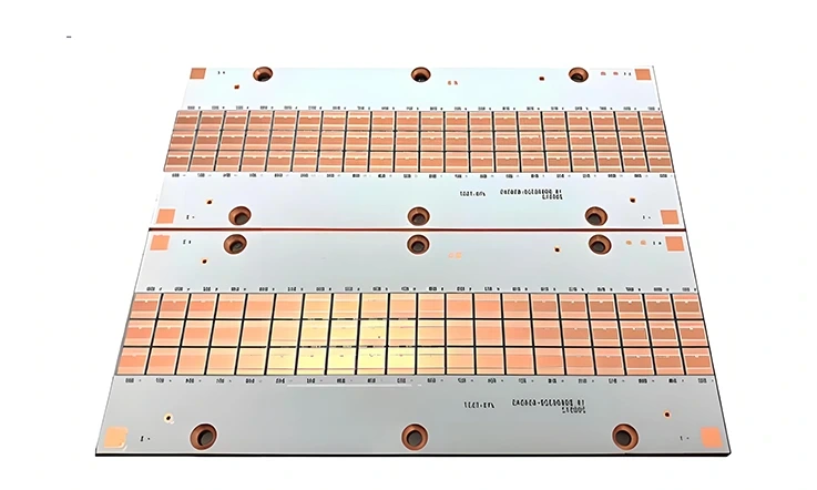
LED Arrays and White Reflective Coating Designs
In LED applications—especially high-density arrays or Chip-on-Board (COB) modules—thermal behavior directly affects light output, color shift, and how long the diodes remain functional. MCPCBs serve by providing a direct thermal path that draws heat away from the active regions of the LEDs. This reduces the chance of temperature-related deterioration and allows the assembly to operate within its intended photometric range for a longer duration.
Efficient Thermal Pathway:
They provide a solid thermal pathway, transferring excess energy away from the light source through a metal base—typically aluminum—which facilitates improved heat dissipation to the ambient environment or a heatsink.
White Reflective Surfaces:
An added dimension in LED system design lies in the surface finish of the PCB. A white solder mask is commonly selected for its ability to reflect visible light, thereby optimizing the luminous efficiency of the LED assembly without relying solely on external lens geometry or housing reflectors.
●The interaction between this reflective layer and the underlying metal substrate must be precisely controlled during manufacturing. Poorly matched thermal coefficients between materials or inconsistent coating thickness—issues addressed by meticulous material selection and process control in fabrication—can lead to heat pockets or discoloration over time, diminishing performance.
Designers also consider the strategic positioning of thermal vias, the layout of surface-mounted LEDs, and current distribution patterns when tailoring MCPCBs for applications such as architectural lighting, automotive lamps, or industrial floodlights. In these uses, reliability over many thousands of hours is more than a specification—it’s a fundamental expectation.
Power Supply and Inverter MCPCB Use Cases
For power electronics—including AC/DC converters, switching-mode power supplies (SMPS), and motor drive inverters—MCPCBs address the dual challenge of managing significant heat dissipation and ensuring robust electrical insulation, often within confined spaces. These boards frequently serve a dual purpose:
●Combined Heatsink and Interface: They can act as both a heat sink and an electrical interface, potentially removing the need for separate mechanical cooling layers while providing a short, efficient thermal path for high-power semiconductor devices.
●Design Considerations for Power Density:Designers must carefully account for thermal resistance across the dielectric layer, the strategic positioning of wide copper pours or planes to handle high currents with minimal loss, and sufficient electrical isolation (creepage and clearance distances) to avoid breakdown at elevated operating voltages.
●Material Choices: The use of various metal core materials, including hybrid substrates such as copper-aluminum combinations, can offer a tailored balance between thermal performance, weight, and cost, depending on the specific application requirements. Realizing the benefits of such specialized constructions often relies on advanced lamination and fabrication techniques available from experienced manufacturers.
| Parameter | Standard FR-4 | MCPCB |
| Max Current Handling (A) | 5 | 15 |
| Dielectric Breakdown Voltage (kV) | 2.5 | 3.5 |
| Thermal Resistance (°C/W) | 1.2 | 0.5 |
| Component Density (W/in²) | 5 | 15 |
In these systems, long-term exposure to heat cycles, especially within enclosed environments like power conversion cabinets or electric vehicle drivetrains, places considerable pressure on both material stability and the reliability of solder joints. This is an area where MCPCBs distinguish themselves—not necessarily by accommodating extreme, short-duration conditions, but by offering a predictable and dependable thermal response across varying loads and extended duty cycles.
Case Study: BMS and EV Inverter Thermal Management with MCPCBs
Electric vehicles (EVs) present a convergence of multiple stress factors for electronic systems: fluctuating electrical currents, wide outdoor temperature changes, persistent mechanical vibrations, and the need for high-voltage isolation—all within a compact and often sealed enclosure. Battery Management Systems (BMS) and power inverters, in particular, represent demanding applications where thermal and electrical design decisions directly impact energy efficiency, system safety, and component durability.
Consider a specific EV application involving a three-phase inverter architecture where an MCPCB was utilized:
Design Features:
●The design leveraged a multilayer MCPCB structure.
●This included copper circuitry for optimized current paths.
●A high-conductivity aluminum base was employed for efficient heat removal from power devices.
●A specialized ceramic-filled dielectric layer was chosen to maintain insulation integrity under repeated thermal stress. The successful fabrication of such a complex stack-up requires precise layer alignment and bonding during the manufacturing process.
●White screen printing was also applied selectively to certain areas requiring visual inspection during maintenance, designed so as not to impede thermal conductivity.
Performance Outcomes:
●The implementation resulted in measurably reduced junction temperatures on key power components (e.g., MOSFETs or IGBTs).
●It contributed to prolonged switching stability for the power semiconductors.
●The design demonstrated consistent dielectric performance throughout more than 1000 thermal cycles, meeting stringent automotive reliability targets.
This application illustrates how MCPCBs are integrated not merely as a standard component, but as an engineered solution, carefully tuned to meet both demanding electrical requirements and challenging environmental constraints.
FAQs:
1.Primary cost drivers for custom MCPCBs?
Material (Al/Cu), thicknesses (core/Cu/dielectric), tolerances, surface finish, order volume.
2.Are flexible MCPCBs a common or viable option for dynamic applications?
Uncommon; durability and consistent thermal contact are challenging. Rigid MCPCBs with flex interconnects are often preferred.
3.How does component reworkability on MCPCBs compare to that on standard FR-4 boards?
More difficult; their high thermal mass requires more intense, localized heat, increasing damage risk during rework.
4.What are the design challenges and implications of using an extremely thin dielectric layer in an MCPCB for maximum thermal transfer?
Significantly lowers thermal resistance, but reduces breakdown voltage, demands tighter manufacturing tolerances, and may increase capacitance.
5.For Chip-on-Board (COB) LEDs, what unique MCPCB design features maximize light output and lifespan beyond general LED guidelines?
Highly reflective solder mask under/around the COB, direct thermal via arrays beneath the chip, minimal dielectric thickness, and efficient current spreading.
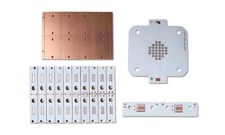
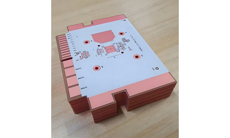
Our services
Metal Core PCB Manufacturing & Assembly


